The two-dimensional electron gas of the In2O3 surface: Enhanced thermopower, electrical transport properties, and its reduction by adsorbates or compensating acceptor doping
Abstract
In2O3 is an n-type transparent semiconducting oxide possessing a surface electron accumulation layer (SEAL) like several other relevant semiconductors, such as InAs, InN, SnO2, and ZnO. Even though the SEAL is within the core of the application of In2O3 in conductometric gas sensors, a consistent set of transport properties of this two-dimensional electron gas (2DEG) is missing in the present literature. To this end, we investigate high quality single-crystalline as well as textured doped and undoped In2O3(111) films grown by plasma-assisted molecular beam epitaxy (PA-MBE) to extract transport properties of the SEAL by means of Hall effect measurements at room temperature while controlling the oxygen adsorbate coverage via illumination. The resulting sheet electron concentration and mobility of the SEAL are cm-2 and cm2/Vs, respectively, both of which get strongly reduced by oxygen-related surface adsorbates from the ambient air. Our transport measurements further demonstrate a systematic reduction of the SEAL by doping In2O3 with the deep compensating bulk acceptors Ni or Mg. This finding is supported by X-ray photoelectron spectroscopy (XPS) measurements of the surface band bending and SEAL electron emission. Quantitative analyses of these XPS results using self-consistent, coupled Schrödinger–Poisson calculations indicate the simultaneous formation of compensating bulk donor defects (likely oxygen vacancies) which almost completely compensate the bulk acceptors. Finally, an enhancement of the thermopower by reduced dimensionality is demonstrated in In2O3: Seebeck coefficient measurements of the surface 2DEG with partially reduced sheet electron concentrations between and cm-2 (corresponding average volume electron concentration between and cm-3) indicate a value enhanced by % compared to that of bulk Sn-doped In2O3 with comparable volume electron concentration.
I Introduction
Indium oxide (In2O3) is a transparent semiconducting oxide, which exhibits inherent n-type conductivity, commonly referred to as unintentional doping (UID). Like the related or SnO2(Nagata et al., 2011), In2O3 possesses a surface electron accumulation layer (SEAL)(King et al., 2009), that lies within the core of In2O3-based conductometric gas sensors for oxygen species.(Rombach et al., 2016) Along with this, In2O3 typically finds applications as a transparent contact in optoelectronic devices, mostly in its highly Sn-doped form, known as ITO(Chae, 2001; Tiwari et al., 2004; Tsai et al., 2016), which can reach electron concentrations as high as . This particular application of In2O3 further benefits from the existence of the SEAL, which favors the formation of Ohmic contacts. This property, nevertheless, indicates that the formation of Schottky contacts—required for several other applications—is hindered by the existence of the SEAL, even for high work function metals like Pt(Michel et al., 2019; von Wenckstern et al., 2014). Tunability of the SEAL is, hence, necessary to both unlock the entire spectrum of potential device applications of In2O3 and tune its gas sensitivity.
Using X-ray photoelectron spectroscopy (XPS) measurements King et al. (2008) demonstrated the existence of a few-nm thick electron accumulation layer at the surface of In2O3 by a downward band bending at the surface of undoped single-crystalline films, in contradiction to previous investigations reporting a surface depletion.(Klein, 2000; Gassenbauer et al., 2006) This discrepancy mainly arose due the difference in the assumed fundamental band gap of In2O3 required for the interpretation of the XPS results: While the optical bandgap of 3.7 eV has been assumed to equal the fundamental one by the authors of Ref. Klein, 2000; Gassenbauer et al., 2006, the authors of Ref. King et al., 2008 have assumed a dipole-forbidden, fundamental band gap of eV — in agreement with state-of-the art ab-initio theory combined with bulk and surface sensitive XPS measurements.(Walsh et al., 2008) A general explanation for the existence of the In2O3 SEAL has been given within the context of the charge neutrality level (CNL), also known as branch point energy. Defect states at the CNL acquire their weight equally from the valence and conduction bands,(Tersoff, 1984) essentially rendering the CNL a demarcation between donor- and acceptorlike defect states. In contrast to most other semiconductors, in the case of In2O3 the CNL lies within the conduction band,(King et al., 2008; Schleife et al., 2009) due to its particular bulk band structure, with a very prominent, low lying conduction band minimum (CBM) at the -point and an almost flat valence band. Donorlike states at the surface of In2O3 pin the surface Fermi level, , slightly below the CNL, causing a downward bending of the conduction and valence bands. Breaking of the translational symmetry of the bulk can give rise to such donorlike surface states.(Mönch, 2001) Besides that, for films exposed to the ambient, the enhanced conductivity of the surface has also been attributed to adsorbates attaching to it; an effect not observed for films that have undergone in situ cleavage of the surface. (Nazarzahdemoafi et al., 2016) The microscopic origin of the SEAL, has been further associated with surface oxygen vacancies acting as doubly ionized shallow donors (Zhang et al., 2013) and their strongly reduced defect formation energy.(Walsh, 2011) Finally, surface In adatoms, which are energetically favored over ,(Wagner et al., 2014) can also act as shallow donors(Davies et al., 2019) and have been experimentally demonstrated on the In2O3(111) surface after a reducing surface preparation [annealing at 300–500 °C in ultra-high vacuum (UHV)].(Wagner et al., 2014)
For 111-oriented films grown by plasma-assisted molecular beam epitaxy (PA-MBE), like the ones studied in the current work, the surface electron concentration has been shown to have a peak value at (King et al., 2009), similar to the results from Schrödinger–Poisson modeling on the SEAL of melt-grown bulk In2O3 single crystal studied in Ref. Nagata et al., 2019. Moreover, angle-resolved photoelectron spectroscopy (ARPES) measurements have confirmed the two-dimensional electron gas (2DEG) nature of the SEAL with sheet electron concentration of after surface preparation at high temperature (by repeated cycles of Ar+ sputtering (500 eV) and annealing at 600 °C in UHV for 1 h)(Zhang et al., 2013) and after surface preparation at intermediate temperature (annealing at 300 °C in UHV for min).(Jovic et al., 2019) Both of the surface preparations employed within those studies are prone to reduce the surface—that is increase the concentration of surface or In adatoms acting as surface donors and, thus, result in a stronger SEAL (i.e. with a higher electron concentration) compared to that of an unprepared sample.
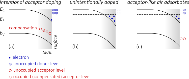
Significant reduction of a SEAL by compensating bulk acceptors has been previously demonstrated in InN by Mg acceptor doping.(Linhart et al., 2012) Previous studies(Papadogianni et al., 2017; Bierwagen and Speck, 2012) have shown that acceptors like Ni and Mg have a compensating effect on the bulk electron transport of In2O3. This effect, however, is revealed after an additional annealing of the material in oxygen, which has been explained by overcompensation of the added acceptors due to the simultaneous formation of donorlike point defects—most likely —during growth:(Papadogianni et al., 2017; Bierwagen and Speck, 2012) The addition of acceptor elements lowers the Fermi energy and, according to Refs. Lany and Zunger, 2007; Limpijumnong et al., 2009, this reduces the formation energy of —thus promoting their incorporation into the crystal lattice. Studies regarding the position of the bulk donor levels in the band gap associated with oxygen vacancies have been rather inconclusive, with some works indicating to have deep donor levels(Lany and Zunger, 2007; Limpijumnong et al., 2009) and others to potentially be shallow donors(Ágoston et al., 2009a; Buckeridge et al., 2018; Chatratin et al., 2019). Whether the annealing completely removed the doping-induced could not be clarified in Refs. Bierwagen and Speck, 2012; Papadogianni et al., 2017. Fig. 1 (a) shows schematically the effect of bulk acceptor doping on the position of the and the band alignment, with emphasis on its impact on the SEAL, assuming neither spontaneous formation of compensating donors nor their removal with a treatment such as oxygen annealing. For comparison, Fig. 1 (b) shows the position of the and band alignment in a UID In2O3.
Early studies on the conductivity of In2O3 at elevated temperatures have already documented its dependence on the oxygen content of the sample environment(Rupprecht, 1954), which is the basis of its application as the active material in conductometric gas sensors. At sufficiently low temperatures, that preclude oxygen diffusion in the lattice, this sensing behavior is related to the surface-acceptor role of adsorbed oxygen species that can reduce the SEAL by electron transfer.(Kim et al., 2013; Berthold et al., 2018) The effect of acceptorlike air adsorbates on the band banding and, hence, occupation of the SEAL is schematically shown in Fig. 1 (c). Such gas sensors are typically (re)activated by heating the sensing material at elevated temperatures (typically a few hundred ° C). Efforts towards a more energy-efficient solution have demonstrated In2O3 gas-sensors operating at room temperature reactivated by ultraviolet (UV) light induced photoreduction (Xirouchaki et al., 1996; Imai et al., 1999; Wang et al., 2007). During photoreduction the illumination forces the desorption of the negatively charged oxygen adsorbates(Wang et al., 2011) through recombination with the photogenerated holes while the photogenerated electrons remain in the In2O3.(Kind et al., 2002) The SEAL sheet conductivity of PA-MBE grown In2O3 films in air has been reported to be in the photoreduced stationary state (under UV illumination)(Rombach et al., 2016) and below with oxygen adsorbates (i.e., without illumination).(Bierwagen et al., 2011a) A reduction of the SEAL in those films by oxygen adsorbates has been independently demonstrated by conductance and XPS measurements.(Rombach et al., 2016; Berthold et al., 2018) However, these earlier works do not provide any information concerning the actual electron concentration at the In2O3 surface.
There have, thus, been no reports regarding the full set of the SEAL transport properties (sheet conductivity and sheet electron concentration) measured with a single technique, after a defined surface treatment, and in a defined environment—as has long been accomplished for ZnO(Grinshpan et al., 1979), for instance. Furthermore, there is no information in the literature concerning the thermoelectric properties of the SEAL. In addition to the strong interest in discovering and understanding the thermoelectric transport properties and mechanisms of such 2DEGs, knowledge of the SEAL properties is necessary for the application aspect of the material, as it enables controllable fine-tuning of the (thermo)electrical behavior of the In2O3 surface.
The current work consistently determines the surface transport properties of In2O3 and demonstrates the intentional and controllable reduction of the sheet electron concentration at the surface of In2O3 by incorporation of the compensating bulk acceptors Ni and Mg or by oxygen surface adsorbates. This is accomplished with the combination of Hall effect transport measurements (with and without UV illumination) and X-ray photoelectron spectroscopy. Supporting self-consistent Schrödinger–Poisson calculations reveal a close compensation of the bulk acceptors by oxygen vacancies even after annealing the samples in oxygen. Finally, the thermoelectric properties of the surface electron accumulation layer are investigated by Seebeck coefficient measurements. As previously demonstrated for ZnO(Shimizu et al., 2016), the 2DEG at the In2O3 surface is shown to also exhibit an increased thermopower in comparison bulk Sn-doped films with comparable volume electron concentration.
II Experiment
For the purposes of this study, high quality (111)-oriented In2O3 has been synthesized by PA-MBE. Single-crystalline UID and Ni-doped films have been grown on quarters of 2” insulating ZrO2:Y (YSZ) (111) substrates, whereas full 2” Al2O3 (0001) (c-plane Al2O3) substrates have been employed for the growth of UID and Mg-doped textured films. After growth, all samples have been further cleaved into smaller pieces with a size of approximately . The total thickness of the films ranges between 350–500 nm. Further details on the growth of the studied samples are reported in Ref. Papadogianni et al., 2017 (single-crystalline) and Ref. Rombach et al., 2016 (textured).
In order to largely remove compensating donors, all samples under study have been annealed in oxygen within a rapid thermal annealing (RTA) system at 800 °C at atmospheric pressure for 60 s. The undoped samples have also been annealed in oxygen to serve as references with comparable characteristics.
For reference measurements, an oxygen plasma treatment of the surface at room temperature was performed in a 13.56 MHz inductively coupled plasma (ICP) reactive ion-etching (RIE) system (Samco Inc., RIE-400iP; process pressure, 0.025 mbar; oxygen flow, 10 standard cubic centimeters per minute; ICP power, 100 W; RIE power, 50 W; treatment time, 5 min) in order to completely deplete surface-near electrons, resulting in an upward surface band bending and complete removal the surface conductivity.(Bierwagen et al., 2011a; Berthold et al., 2016) During this treatment, a high density of reactive oxygen species attach to the In2O3 surface, removing electrons from the In2O3 to form negatively charged adsorbates.(Berthold et al., 2016) We found this adsorbate layer to be stable against UV-illumination and to be removable only by annealing the material.
The electrical sheet conductivity of the films under study is determined by sheet resistance measurements in the commonly used van der Pauw (vdP) arrangement. In combination with Hall effect measurements, which directly provide the sheet electron concentration, this helps identify the Hall electron mobility of the samples.
Since the measurements throughout this work are performed in ambient environment, oxygen species from the air are expected to adsorb and alter the transport properties of the SEAL. To circumvent this effect, the samples under study have been exposed to UV illumination to force desorption of those species. A light emitting diode (LED) that can generate up to 12 mW ultraviolet (UV) A radiation with a wavelength of 400 nm is utilized for this purpose. The corresponding photon energy of 3.1 eV is above the fundamental, dipole forbidden bandgap and below the onset of strong optical absorption.(Walsh et al., 2008) The associated penetration depth in In2O3 is 1 μm,(Irmscher et al., 2013) i.e., larger than the thickness of the investigated films. For most measurements the LED is operated at a current of 13 mA, which corresponds to approximately 8 mW of optical power, and the illuminated area nominally covers the entire sample surface. This corresponds to a photon flux of approximately . Due to the UV-induced desorption of species the conductivity of the surface—and thus the total conductivity of the film—increases with time until it starts saturating once a desorption–adsorption equilibrium has been reached. Representative desorption/adsorption cycles due to UV on/UV off periods can be found in Ref. Rombach et al., 2016. For the measurements to be reproducible, all samples are exposed to UV for approximately 10 minutes, which has been found sufficient to obtain desorption-adsorption equilibrium.
For the X-ray Photoelectron Spectroscopy (XPS) measurements, the samples were mounted onto Ta sample holders, with the In2O3 layer electrically grounded, and inserted into an ultra-high vacuum (UHV) system for surface analysis. The measurements were performed—after preparation of the surface with UV illumination in vacuum at room temperature—in normal emission using monochromated AlKα () radiation and a hemispherical electron analyzer. More details about the setup and the experimental conditions used for this study can be found in Ref. Himmerlich et al., 2007. The binding energy scale and the position of the Fermi level are regularly calibrated for clean metal reference samples and the data analysis was performed in analogy to the studies of UID and Mg-doped In2O3 films in Ref. Berthold et al., 2016. The region around the was measured with an extended integration time.
Finally, the acquisition of the thermopower, otherwise known as Seebeck coefficient, was performed as described in detail for In2O3 in Ref. Preissler et al., 2013. The Seebeck coefficient of the SEAL has been calculated by the multilayer method described in Refs. Baron et al., 1969; Bierwagen et al., 2011b and then matched to the corresponding 2D electron concentrations—determined by the Hall effect—for measurements with the same sheet resistance (adjusted by proper UV illumination) using the van der Pauw method. This is done because the Seebeck and Hall effect measurements are performed in two separate systems and the sheet resistance is the only property that can be measured in both setups and ensure same surface conditions.
III Results and discussion
III.1 Transport properties of the adsorbate-attenuated and unattenuated SEAL extracted by the multilayer method
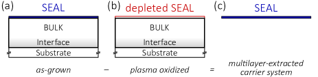
In order to extract the transport properties of the surface carrier system of In2O3 the multilayer method described in Refs. Baron et al., 1969; Bierwagen et al., 2011b will be employed. Essentially, since all transport systems in our films (depicted in Fig. 2(a)) are connected in parallel, the total sheet conductivity of the film will be the sum of the separate sheet conductivities of the carrier systems comprising it
| (1) |
where the subscripts indicate the bulk (B), interface (I), and surface (S) sheet conductivity. Let us assume the case depicted in Fig. 2 with two films, (a) and (b), comprising of the same carrier systems—bulk and interface—with the exception of the SEAL, which is not present in film (b). Based on the model described, the sheet conductivity of the carrier system these films differ by, (c), could be extracted by subtracting the total sheet conductivities of the two films. A technique to deplete the SEAL is thus required for this method to be applied.
The plasma oxidation of the surface described in the experimental part can provide samples with depleted SEAL. This indicates that the sheet conductivity of a plasma oxidized sample equals . Combining this with the multilayer model of Refs. Baron et al., 1969; Bierwagen et al., 2011b allows one to extract not only the sheet conductivity, but also the entire set of transport properties of the SEAL by performing Hall effect measurements on an unintentionally doped (UID) sample of In2O3 before and after plasma treatment. As an example, one can extract the sheet conductivity of the SEAL as
| (2) |
where a.g. is used to denote the untreated (besides oxygen annealing), as-grown state of the film. This of course would correspond to an upper estimate of the sheet conductivity of the SEAL with the effect of present air adsorbates (superscript “w/ ads.”). In our UID, single crystalline film we found such a SEAL to feature a sheet conductivity of , which is significantly lower than that of the photoreduced SEAL () in Ref. Rombach et al., 2016 and suggests that the oxygen adsorbates from the air almost completely deplete the SEAL.
Since the plasma oxidation of the surface could potentially deplete part of the bulk, the extracted sheet conductivity from Eq. 2 could contain the near surface bulk conductivity that got depleted. In order to avoid these effects being reflected on the extracted SEAL transport properties, one can extract the sheet conductivity of the adsorbate-free (superscript “w/o ads.”) SEAL as follows
| (3) |
assuming the UV light exposure to remove all surface adsorbates by photoreduction and full depletion of the SEAL in the dark by adsorbed oxygen species. At this point, it should be pointed out that the high penetration depth of the UV illumination could induce photoconduction in the bulk of the material. Examination of the conductivity change upon UV illumination of an undoped In2O3 film, whose surface had been depleted by undergoing the plasma oxidation process, showed a sudden drop of the sheet conductivity by , which amounts up to 7% of the total change in sheet conductivity by the UV as observed in the untreated sample. This bulk photoconduction effect is also excluded by the difference method of Eq. 3.
The method described in Refs. Baron et al., 1969; Bierwagen et al., 2011b allows for the extraction of the full set of SEAL transport properties. According to these, the mobility and Seebeck coefficient can both be extracted in a similar manner using respectively
| (4) |
| (5) |
Finally, the sheet (2D) electron concentration of the SEAL without the effect of air adsorbates can be easily calculated based on the results of Eqs. 3 and 4 as
| (6) |
where is the elementary charge. Based on the equations above, the SEAL of an undoped single-crystalline In2O3 film has been found to exhibit a sheet conductivity of , a sheet electron concentration of , and a Hall electron mobility of without the effect of air adsorbates.
III.2 Intentional attenuation by compensating acceptor doping
Electrical transport
Figure 3 depicts the SEAL transport properties extracted from the Hall measurements by Eqs. (3, 4, and 6) of a series of single-crystalline Ni-doped (blue circles) and textured Mg-doped (red stars) films, along with their dedicated unintentionally doped samples. Increasing compensating doping leads—as expected—to a decrease in the extracted sheet conductivity of the SEAL for both types of dopants and substrates. A Ni concentration of approximately —which is comparable to the peak surface electron concentration of Ref. King et al., 2009—has a significant effect on it, whereas a similar concentration of Mg, does not substantially affect the SEAL transport properties. Higher Ni-doping seems to deplete most of the surface carriers, reaching SEAL sheet conductivities as low as and a very low Hall mobility, that does not allow for the extraction of a meaningful surface electron concentration. Interestingly, an even higher Mg concentration of does not fully deplete the SEAL. Besides the doping ranges presented in Fig. 3, a higher Ni doped sample on YSZ (111) with has been also studied and shown (in Ref. Papadogianni et al., 2017) to be insulating, in which case all carrier systems—including the SEAL—have been fully depleted.
To compare with the degree of depletion attained unintentionally by air adsorbates, the data in Fig. 3 represented by full circles demonstrate the sheet conductivity of one UID and one lightly Ni-doped sample that have been measured under dark conditions. The effect of air adsorbates with an acceptorlike behavior is evidently intense, as they decrease the sheet conductivity of the films by two orders of magnitude.
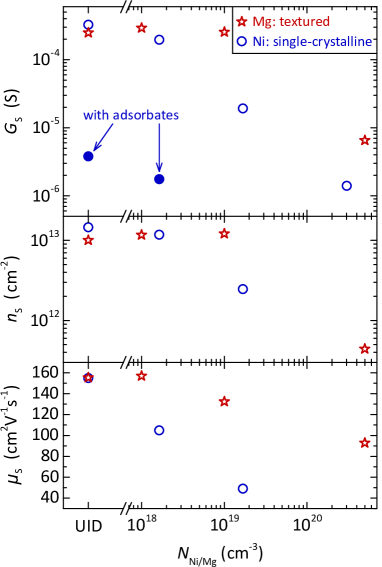
Both the sheet electron concentration and mobility of the SEAL decrease with increasing acceptor concentration, as would have been anticipated for compensating dopants and the addition of charged scattering centers.
However, there seems to be a different doping threshold between the two sample series, which results in stronger or full depletion of the SEAL, and they exhibit different mobilities. In particular, the SEAL mobility of the single crystalline Ni-doped films is significantly lower than the mobility of the Mg-doped ones on c-Al2O3, which feature grain boundaries. This is a rather unexpected result, however the lower electron concentration of the Ni-doped series could possibly be attributed to the fact that YSZ is an oxygen conductor, and therefore oxygen from the substrate could diffuse to the surface and deplete the SEAL. Moreover, the position of the deep acceptors in the band gap and, hence, the probability to compensate SEAL electrons, can differ.
X-ray photoelectron spectroscopy
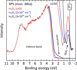
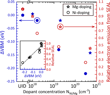
To relate the electrical transport results to the band structure and surface band bending, XPS measurements have been performed on both the Ni-doped single-crystalline and the Mg-doped textured samples. The method probes the topmost few nanometers at the surface of the film. Figure 4 illustrates the valence band spectrum obtained by XPS for the single-crystalline UID (red) and the Ni-doped samples with and (blue and black respectively), after illumination with UV in vacuum, to best represent the state of the films during the transport measurements. The binding energy is presented with respect to the position of the Fermi level. The broad distribution between 10 and 3 eV originates from emission of valence band electrons(Erhart et al., 2007; King et al., 2009; Himmerlich et al., 2012), whereas the feature just below the is due to partial occupation of conduction band states of the SEAL (King et al., 2008; Rombach et al., 2016) sustained by the distinct downward bending of the electronic bands at the surface(King et al., 2009). When Ni acceptors are introduced into the film, the valence band maximum (VBM) shifts towards lower binding energy for higher Ni concentrations. The same effect is observed for the core level energies. Both these shifts consistently indicate a lowering of the surface Fermi level with increasing Ni concentration. At the same time, the emission of electrons near the from the SEAL is significantly lowered. The same effect is also observed for the Mg-doped In2O3 films. Furthermore, for the highest Ni concentration, an enhanced emission is observed above the VB maximum, which indicates the formation of intragap states. Such states above the VBM in In2O3 have been attributed to the existence of oxygen vacancies(Mizuno et al., 1997; Tanaka et al., 2002; Ágoston et al., 2009b). Their appearance at high Ni concentrations could be an indication that the incorporation of acceptors leads to a partial charge compensation by formation of additional oxygen vacancies. However, this effect has not been observed for highly Mg-doped In2O3 films(Berthold et al., 2016).
The determination of the absolute energy of the VBM and the difference between surface and conduction band minimum by XPS is not straightforward. We discuss our quantitative evaluation in the supplemental material, which results in a value of for UID In2O3. The change in band edge position, however, can be determined by characterizing the energy offset in XPS. We have compared the change of VBM (ΔVBM) for Ni- and Mg-doped films with varying acceptor concentrations. In addition, the area of the emission near the is used as a quantitative measure of the electrons in the SEAL(Berthold et al., 2018). Both values—ΔVBM and the relative reduction of the SEAL compared to UID films—are plotted as a function of the Ni and Mg concentration in Fig. 5. It is evident that there is a correlation among the increasing acceptor concentration, the shift of VB edge towards the , and the reduction of surface electron concentration. Moreover, a roughly linear relation between ΔVBM and the relative electron emission from SEAL is observed (inset of Fig. 5). In accordance with the electrical transport measurements, Ni-doping is shown to induce stronger changes in the electronic properties in comparison to the Mg-doping. Nonetheless, a significant depletion of the SEAL has been achieved, i.e. down to 26 % of that of the UID In2O3 for the highest Ni concentration. At this Ni concentration, however, transport measurements indicated a stronger reduction of the SEAL (conductance decrease to less than 1 % of that of the UID In2O3). We tentatively attribute this discrepancy to a residual O-adsorbate coverage of the adsorption-desorption equilibrium during the transport measurements under UV illumination in air.
Self-consistent Schrödinger–Poisson calculations of the near-surface potential and electron density profiles
| Nº | Acceptor type | |||||||
|---|---|---|---|---|---|---|---|---|
| (cm-3) | (cm-3) | (cm-3) | (eV) | (eV) | (cm-2) | (cm-2) | ||
| i | — | — | 0.047 | -0.600 | (A) | (B) | ||
| ii | mid-gap | 1.388 | -0.380 | (0.26B) | ||||
| iii | mid-gap | 1.431 | (A) | (0.26B) | ||||
| iv | shallow | 2.762 | -0.380 | (A) | ||||
| v | mid-gap | 1.449 | -0.380 | (A) | ||||
| vi | shallow | 2.762 | -0.380 | (A) | ||||
| vii | mid-gap | 1.274 | -0.380 | (A) | ||||
| viii | shallow | 2.697 | -0.380 | (0.26B) | ||||
| ix | mid-gap | 1.212 | -0.380 | (0.26B) | ||||
| x | mid-gap | 1.281 | -0.380 | (0.26B) | ||||
| xi | mid-gap | 1.351 | -0.380 | (0.26B) |
To better understand the near-surface band and electron density profiles in the In2O3 films we have performed self-consistent Schrödinger–Poisson calculations varying the acceptor concentration and using the experimentally determined parameters obtained from electron transport measurements and X-ray photoelectron spectroscopy as constraints. For the Poisson equation, the Dirichlet boundary conditions (i.e., fixed surface potential relative to the bulk Fermi level position) are used. We assume the full ionization of donors present in the samples, whereas for acceptors the incomplete ionization is also considered by defining the ionization energy level relative to the valence band edge. The effect of the conduction band nonparabolicity is also accounted for, and the band structure parameters as well as the dielectric parameters have been taken from Ref. Feneberg et al., 2016. The net surface charge , corresponding to the difference of the 2D concentration of charged surface donors and acceptors schematically shown in Fig. 1(c), is calculated from the charge neutrality condition applied to the entire sample.
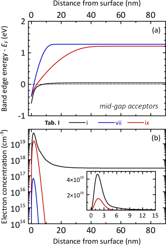
Table 1 and Figure 6 summarize the major parameters and profiles based on calculations under various assumptions as described next.
Initially (Tab. 1, case i) the from the XPS results corresponding to the UID sample, along with the corresponding to a reasonable bulk donor concentration of are used to calculate the SEAL concentration of the UID sample, . The result of matches very well the experimentally extracted results from the Hall effect measurements. is assumed to correspond to singly charged donors, ignoring the possible contribution from doubly charged donors, like as previously discussed.
Next, acceptor doping is considered, where acceptors are not assumed to induce the generation of compensating donors—i.e. the donor concentration of is forced to be the same as for the unintentionally doped film in case (i). If the and from the XPS results for the sample doped with are considered (0.26B) (case ii), the result would be a reduced surface states concentration, , and an acceptor concentration, , that is significantly lower than the actual doping value. Alternatively, (case iii) fixing at the value (A) of the UID sample, the predicted surface Fermi energy shift of only compared to the UID case does not match the experimental results. If the is kept constant at value (A) and the band edge shift from XPS are simultaneously considered (case iv), the result would correspond to complete depletion of the SEAL, even for significantly lower acceptor concentrations than the actual . This result holds true irrespective of the dopant position in the band gap, i.e. shallow (case iv) or mid-gap (case v) acceptor level of Ni. However, as both the transport measurements and the XPS results have revealed, the SEAL is still present for such low acceptor concentrations. Thus, spontaneous generation of compensating donors upon introduction of the acceptors has to be considered.
Cases (vi) and (vii) show that even if the actual acceptor concentration, , and corresponding donor generation are considered, a fixed at the value (A) of the UID sample would predict the respective SEAL to be fully depleted, for both, shallow or mid-gap acceptor levels. Hence, the surface states concentration needs to be decreased in order to reproduce the experimental results.
Fixing the acceptor concentration at the intentional Ni-doping level of , a comparable and, in fact, only slightly lower donor concentration (cases viii and ix) has to be considered to result in corresponding SEAL concentration measured by XPS. Once again, the position of the acceptor levels in the band gap is of minimal significance to these results (viii, ix), with the and only being slightly affected. Assuming deep acceptors—as there are indications that this is the case(Raebiger et al., 2009), even though they are not expected to be positioned in the middle of the band gap—and varying their concentrations by one order of magnitude at each step (cases ix-xi), we showcase that the relevant parameter for the reduction of the SEAL is . For shallow acceptors the does not change at all (see supporting information).
Even though these calculations rely on certain assumptions and constraints, they allow to deduce important trends. The most important band edge and electron concentration profiles of Tab. 1 are plotted in Fig. 6. The inset shows the carrier distribution in a linear scale for three different cases, matching the relative emission of the SEAL derived from XPS, and highlights the reduction of surface electron concentration when Ni or Mg acceptors are incorporated into the In2O3 layers. Integration of the profile in the inset of Fig. 6 corresponding to the acceptor-doped case (ix) indicates that the majority (approximately 90%) of the SEAL carriers are lying within 3 nm from the surface.
Consequently, no complete depletion of the In2O3 SEAL is achieved by acceptors at these doping concentrations, due to the spontaneous formation of compensating donors. This conclusion contrasts the findings in Mg-doped InN(Linhart et al., 2012), where the lack of compensating donors results in the immense reduction of the SEAL. Nevertheless, the obtained results are promising towards the tunability of the In2O3 surface properties and the expansion of its potential device applications.
III.3 Enhanced thermopower in the SEAL 2DEG
For the determination of the Seebeck coefficient of the In2O3 surface, the Mg-doped sample with —with an intact SEAL and almost fully depleted parallel carrier systems—has been utilized. The effect of a weak parallel interface system has been taken into consideration and excluded using the multilayer method described previously, and specifically Eq. 5. Since the oxygen plasma treatment did not essentially affect the transport properties of this particular sample, the Seebeck coefficient was ultimately extracted from the measurements of the dark and photoreduced states of the as-grown film. The sheet electron concentration of the films has been gradually modulated using UV illumination with varying optical power between 1 and 12 mW and corresponding waiting time, which results in adsorbed, acceptorlike, oxygen species between high and low steady-state coverage. As shown in Fig. 7 (top), the Seebeck coefficient of the SEAL is negative, as expected for carrier systems with their majority carriers being electrons, and exhibits a decreasing magnitude with increasing electron concentration. Due to limitations of the external UV illumination at the Seebeck setup, it has not been possible to obtain a state of the In2O3 SEAL with higher electron concentration.
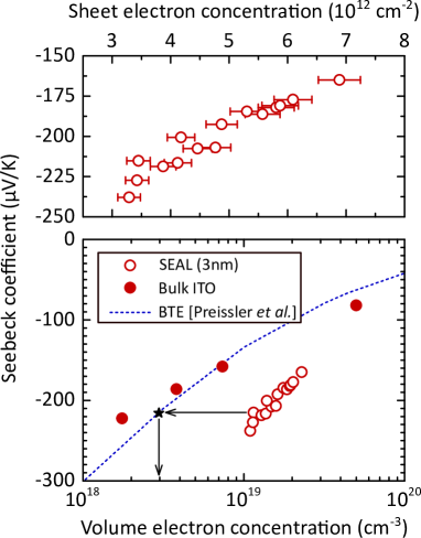
According to Ref. Shimizu et al., 2016, the Seebeck coefficient of a two-dimensional electron gas (2DEG)—in that case ZnO—exhibits an increased absolute value, in comparison to that of a three-dimensional electron gas (3DEG), if the semiconductor is well degenerate. This effect is also displayed in Fig. 7, where the Seebeck coefficient of the SEAL (2DEG) is compared to the experimental values of four ITO films (3DEG) as well as the theoretical curve of Ref. Preissler et al., 2013 based on the solution of the Boltzmann transport equation (BTE) for similar volume electron concentrations as that of the SEAL. This comparison yields a % larger Seebeck coefficient of the surface 2DEG compared to a bulk 3DEG with comparable volume electron concentration. The average volume electron concentration of the SEAL has been calculated assuming that the vast majority of the carriers lie within a 3 nm thick system (cf. SP calculations of case (ix) in Tab. 1 and Fig. 6 for similar sheet electron concentration). That of the homogeneously Sn-doped ITO films has been obtained from Hall effect measurements and the film thickness.
Approaching it from a different perspective, if the Seebeck coefficient of the SEAL would coincide with the BTE solution of a bulk system in Fig. 7, as indicated by the black arrow for one of the data points, the corresponding average volume electron concentration of the SEAL would be significantly lower. As explained in detail in Ref. Papadogianni et al., 2015, the sheet and volume electron concentrations of a carrier system can be used to estimate its effective thickness, . If the volume electron concentration dictated by the BTE curve, which is valid for bulk systems, is combined with the sheet electron concentration directly measured by Hall, the resulting SEAL thicknesses would vary between . This is a clear overestimation in comparison to both the findings of the SP calculations in Fig. 6 and previous works(King et al., 2008; Nagata et al., 2019, 2017), again indicating an enhanced thermopower of the SEAL.
IV Summary and Conclusion
In this work we have experimentally determined the transport properties of the In2O3 surface electron accumulation layer by Hall effect measurements through applying a dual-layer model in combination with plasma oxidation treatments of the surface. Oxygen adsorbates from the ambient air almost completely deplete the SEAL of an unintentionally doped film reducing its sheet conductivity to . Illuminating the surface with UV radiation largely removed the oxygen adsorbates, resulting in a SEAL with a sheet conductivity of , a sheet electron concentration of , and a Hall electron mobility of . We further demonstrated a gradual reduction of this SEAL by increasing compensating bulk acceptor doping with two different elements, namely Ni and Mg, and achieved nearly complete depletion with doping. The gradual depletion of the SEAL with doping concentration has been confirmed by XPS measurements, able to determine the position of the valence band maximum and SEAL peak area close to the Fermi level. These results were further supported by Schrödinger–Poisson calculations, which clearly show that the introduction of acceptors in the In2O3 results in the subsequent generation of comparable concentrations of compensating donors. This result holds true irrespective of the position of the acceptors in the band gap, i.e. whether the corresponding levels are deep (mid-gap) or shallow. This mechanism hinders the complete depletion of the In2O3 SEAL. However, our results showing significant attenuation of the surface with acceptor doping are still valuable for device applications requiring tunable surface transport properties. Ultimately, the thermopower of the In2O3 SEAL is investigated. In agreement with previous studies on ZnO, the Seebeck coefficient of the 2DEG at the In2O3 surface is shown to be enhanced by % in comparison to the 3DEG with comparable volume electron concentration in bulk ITO films.
Acknowledgment
We would like to thank Y. Takagaki for critically reading this manuscript, F. Gutsche for technical support with the Seebeck setup, and W. Anders for the oxygen plasma treatment of the samples. This study was performed in the framework of GraFOx, a Leibniz ScienceCampus partially funded by the Leibniz association. We are grateful for the financial support by the Deutsche Forschungsgemeinschaft (grants BI 1754/1-1 and HI 1800/1-1).
References
- Nagata et al. (2011) T. Nagata, O. Bierwagen, M. E. White, M. Y. Tsai, Y. Yamashita, H. Yoshikawa, N. Ohashi, K. Kobayashi, T. Chikyow, and J. S. Speck, Applied Physics Letters 98, 232107 (2011).
- King et al. (2009) P. D. C. King, T. D. Veal, F. Fuchs, C. Y. Wang, D. J. Payne, A. Bourlange, H. Zhang, G. R. Bell, V. Cimalla, O. Ambacher, R. G. Egdell, F. Bechstedt, and C. F. McConville, Phys. Rev. B 79, 205211 (2009).
- Rombach et al. (2016) J. Rombach, A. Papadogianni, M. Mischo, V. Cimalla, L. Kirste, O. Ambacher, T. Berthold, S. Krischok, M. Himmerlich, S. Selve, and O. Bierwagen, Sens. Actuators B 236, 909 (2016).
- Chae (2001) G. S. Chae, Jpn. J. Appl. Phys. 40, 1282 (2001).
- Tiwari et al. (2004) A. N. Tiwari, G. Khrypunov, F. Kurdzesau, D. L. Bätzner, A. Romeo, and H. Zogg, Prog. Photov. 12, 33 (2004).
- Tsai et al. (2016) M. Y. Tsai, O. Bierwagen, and J. S. Speck, Thin Solid Films 605, 186 (2016).
- Michel et al. (2019) J. Michel, D. Splith, J. Rombach, A. Papadogianni, T. Berthold, S. Krischok, M. Grundmann, O. Bierwagen, H. von Wenckstern, and M. Himmerlich, ACS Applied Materials & Interfaces 11, 27073 (2019).
- von Wenckstern et al. (2014) H. von Wenckstern, D. Splith, F. Schmidt, M. Grundmann, O. Bierwagen, and J. S. Speck, APL Materials 2, 046104 (2014).
- King et al. (2008) P. D. C. King, T. D. Veal, D. J. Payne, A. Bourlange, R. G. Egdell, and C. F. McConville, Phys. Rev. Lett. 101, 116808 (2008).
- Klein (2000) A. Klein, Appl. Phys. Lett. 77, 2009 (2000).
- Gassenbauer et al. (2006) Y. Gassenbauer, R. Schafranek, A. Klein, S. Zafeiratos, M. Hävecker, A. Knop-Gericke, and R. Schlögl, Phys. Rev. B. 73, 245312 (2006).
- Walsh et al. (2008) A. Walsh, J. L. F. D. Silva, S.-H. Wei, C. Korber, A. Klein, L. F. J. Piper, A. DeMasi, K. E. Smith, G. Panaccione, P. Torelli, D. J. Payne, A. Bourlange, and R. G. Egdell, Physical Review Letters 100, 167402 (2008).
- Tersoff (1984) J. Tersoff, Phys. Rev. Lett. 52, 465 (1984).
- Schleife et al. (2009) A. Schleife, F. Fuchs, C. Rödl, J. Furthmüller, and F. Bechstedt, Applied Physics Letters 94, 012104 (2009).
- Mönch (2001) W. Mönch, Semiconductor Surfaces and Interfaces (Springer, 2001).
- Nazarzahdemoafi et al. (2016) M. Nazarzahdemoafi, F. Titze, S. Machulik, C. Janowitz, Z. Galazka, R. Manzke, and M. Mulazzi, Phys. Rev. B 93, 081303 (2016).
- Zhang et al. (2013) K. H. L. Zhang, R. G. Egdell, F. Offi, S. Iacobucci, L. Petaccia, S. Gorovikov, and P. D. C. King, Phys. Rev. Lett. 110, 056803 (2013).
- Walsh (2011) A. Walsh, Applied Physics Letters 98, 261910 (2011).
- Wagner et al. (2014) M. Wagner, S. Seiler, B. Meyer, L. A. Boatner, M. Schmid, and U. Diebold, Advanced Materials Interfaces 1, 1400289 (2014).
- Davies et al. (2019) D. W. Davies, A. Walsh, J. J. Mudd, C. F. McConville, A. Regoutz, J. M. Kahk, D. J. Payne, V. R. Dhanak, D. Hesp, K. Pussi, T.-L. Lee, R. G. Egdell, and K. H. L. Zhang, The Journal of Physical Chemistry C 123, 1700 (2019).
- Nagata et al. (2019) T. Nagata, O. Bierwagen, Z. Galazka, M. Imura, S. Ueda, Y. Yamashita, and T. Chikyow, Japanese Journal of Applied Physics 58, SDDG06 (2019).
- Jovic et al. (2019) V. Jovic, S. Moser, A. Papadogianni, R. J. Koch, A. Rossi, C. Jozwiak, A. Bostwick, E. Rotenberg, J. V. Kennedy, O. Bierwagen, and K. E. Smith, Small , 1903321 (2019).
- Linhart et al. (2012) W. M. Linhart, J. Chai, R. J. H. Morris, M. G. Dowsett, C. F. McConville, S. M. Durbin, and T. D. Veal, Phys. Rev. Lett. 109, 247605 (2012).
- Papadogianni et al. (2017) A. Papadogianni, L. Kirste, and O. Bierwagen, Appl. Phys. Lett. 111, 262103 (2017).
- Bierwagen and Speck (2012) O. Bierwagen and J. S. Speck, Appl. Phys. Lett. 101, 102107 (2012).
- Lany and Zunger (2007) S. Lany and A. Zunger, Phys. Rev. Lett. 98, 045501 (2007).
- Limpijumnong et al. (2009) S. Limpijumnong, P. Reunchan, A. Janotti, and C. G. Van de Walle, Phys. Rev. B 80, 193202 (2009).
- Ágoston et al. (2009a) P. Ágoston, K. Albe, R. M. Nieminen, and M. J. Puska, Physical Review Letters 103, 245501 (2009a).
- Buckeridge et al. (2018) J. Buckeridge, C. R. A. Catlow, M. R. Farrow, A. J. Logsdail, D. O. Scanlon, T. W. Keal, P. Sherwood, S. M. Woodley, A. A. Sokol, and A. Walsh, Phys. Rev. Materials 2, 054604 (2018).
- Chatratin et al. (2019) I. Chatratin, F. P. Sabino, P. Reunchan, S. Limpijumnong, J. B. Varley, C. G. Van de Walle, and A. Janotti, Phys. Rev. Materials 3, 074604 (2019).
- Rupprecht (1954) G. Rupprecht, Zeitschrift für Physik 139, 504 (1954).
- Kim et al. (2013) I.-D. Kim, A. Rothschild, and H. L. Tuller, Acta Materialia 61, 974 (2013).
- Berthold et al. (2018) T. Berthold, S. Katzer, J. Rombach, S. Krischok, O. Bierwagen, and M. Himmerlich, Physica Status Solidi B: Basic Solid State Physics 255, 1700324 (2018).
- Xirouchaki et al. (1996) C. Xirouchaki, G. Kiriakidis, T. F. Pedersen, and H. Fritzsche, J. Appl. Phys. 79, 9349 (1996).
- Imai et al. (1999) H. Imai, A. Tominaga, H. Hirashima, M. Toki, and N. Asakuma, J. Appl. Phys. 85, 203 (1999).
- Wang et al. (2007) C. Y. Wang, V. Cimalla, T. Kups, C.-C. Röhlig, T. Stauden, O. Ambacher, M. Kunzer, T. Passow, W. Schirmacher, W. Pletschen, K. Köhler, and J. Wagner, Appl. Phys. Lett. 91, 103509 (2007).
- Wang et al. (2011) C. Wang, R. Becker, T. Passow, W. Pletschen, K. Köhler, V. Cimalla, and O. Ambacher, Sensors and Actuators B: Chemical 152, 235 (2011).
- Kind et al. (2002) H. Kind, H. Yan, B. Messer, M. Law, and P. Yang, Advanced Materials 14, 158 (2002).
- Bierwagen et al. (2011a) O. Bierwagen, J. S. Speck, T. Nagata, T. Chikyow, Y. Yamashita, H. Yoshikawa, and K. Kobayashi, Appl. Phys. Lett. 98, 172101 (2011a).
- Grinshpan et al. (1979) Y. Grinshpan, M. Nitzan, and Y. Goldstein, Phys. Rev. B 19, 1098 (1979).
- Shimizu et al. (2016) S. Shimizu, M. S. Bahramy, T. Iizuka, S. Ono, K. Miwa, Y. Tokura, and Y. Iwasa, Proceedings of the National Academy of Sciences 113, 6438 (2016).
- Berthold et al. (2016) T. Berthold, J. Rombach, T. Stauden, V. Polyakov, V. Cimalla, S. Krischok, O. Bierwagen, and M. Himmerlich, J. Appl. Phys. 120, 245301 (2016).
- Irmscher et al. (2013) K. Irmscher, M. Naumann, M. Pietsch, Z. Galazka, R. Uecker, T. Schulz, R. Schewski, M. Albrecht, and R. Fornari, physica status solidi (a) 211, 54 (2013).
- Himmerlich et al. (2007) M. Himmerlich, S. Krischok, V. Lebedev, O. Ambacher, and J. Schaefer, Journal of Crystal Growth 306, 6 (2007).
- Preissler et al. (2013) N. Preissler, O. Bierwagen, A. T. Ramu, and J. S. Speck, Phys. Rev. B 88, 085305 (2013).
- Baron et al. (1969) R. Baron, G. A. Shifrin, O. J. Marsh, and J. W. Mayer, J. Appl. Phys. 40, 3702 (1969).
- Bierwagen et al. (2011b) O. Bierwagen, S. Choi, and J. S. Speck, Phys. Rev. B 84, 235302 (2011b).
- Erhart et al. (2007) P. Erhart, A. Klein, R. G. Egdell, and K. Albe, Phys. Rev. B 75, 153205 (2007).
- Himmerlich et al. (2012) M. Himmerlich, C. Y. Wang, V. Cimalla, O. Ambacher, and S. Krischok, Journal of Applied Physics 111, 093704 (2012).
- Mizuno et al. (1997) M. Mizuno, T. Miyamoto, T. Ohnishi, and H. Hayashi, Japanese Journal of Applied Physics 36, 3408 (1997).
- Tanaka et al. (2002) I. Tanaka, F. Oba, K. Tatsumi, M. Kunisu, M. Nakano, and H. Adachi, Mater. Trans. 43, 1426 (2002).
- Ágoston et al. (2009b) P. Ágoston, P. Erhart, A. Klein, and K. Albe, Journal of Physics: Condensed Matter 21, 455801 (2009b).
- Feneberg et al. (2016) M. Feneberg, J. Nixdorf, C. Lidig, R. Goldhahn, Z. Galazka, O. Bierwagen, and J. S. Speck, Phys. Rev. B 93, 045203 (2016).
- Raebiger et al. (2009) H. Raebiger, S. Lany, and A. Zunger, Phys. Rev. B 79, 165202 (2009).
- Papadogianni et al. (2015) A. Papadogianni, M. E. White, J. S. Speck, Z. Galazka, and O. Bierwagen, Applied Physics Letters 107, 252105 (2015).
- Nagata et al. (2017) T. Nagata, O. Bierwagen, Z. Galazka, M. Imura, S. Ueda, H. Yoshikawa, Y. Yamashita, and T. Chikyow, Applied Physics Express 10, 011102 (2017).