Are We Susceptible to Rowhammer?
An End-to-End Methodology for Cloud Providers
Abstract
Cloud providers are concerned that Rowhammer poses a potentially critical threat to their servers, yet today they lack a systematic way to test whether the DRAM used in their servers is vulnerable to Rowhammer attacks. This paper presents an end-to-end methodology to determine if cloud servers are susceptible to these attacks. With our methodology, a cloud provider can construct worst-case testing conditions for DRAM.
We apply our methodology to three classes of servers from a major cloud provider. Our findings show that none of the CPU instruction sequences used in prior work to mount Rowhammer attacks create worst-case DRAM testing conditions. To address this limitation, we develop an instruction sequence that leverages microarchitectural side-effects to “hammer” DRAM at a near-optimal rate on modern Intel Skylake and Cascade Lake platforms. We also design a DDR4 fault injector that can reverse engineer row adjacency for any DDR4 DIMM. When applied to our cloud provider’s DIMMs, we find that DRAM rows do not always follow a linear map.
I Introduction
The consequences of a large-scale security compromise of a cloud provider cannot be overstated. An increasing number of banks, hospitals, stores, factories, and universities depend upon cloud resources for their day-to-day activities. Users store important and private data in the cloud, including tax returns, health records, e-mail, and backups. Home devices and home automation are also becoming reliant on cloud infrastructure. An attack that steals or deletes data, or performs a large-scale denial of service (DoS) attack on the cloud, would be catastrophic to both cloud providers and customers.
Today’s DRAM is vulnerable to memory disturbance errors: a high rate of accesses to the same address in DRAM flips bits in data stored in nearby addresses [69]. Rowhammer attacks generate adversarial workloads that exploit disturbance errors to flip the value of security-critical bits, such as an OS’s page table entries [97, 32], a browser’s isolation sandbox [32], a CPU’s isolation mechanism [59], an encryption key [97], or a CPU instruction opcode [36]. Even worse, mounting Rowhammer requires no special privilege: attacks have been demonstrated by running user-level code [32, 97], JavaScript programs [13, 37], and even by sending RDMA network packets [106, 83]. Because all DRAM is potentially susceptible, Rowhammer attacks are an easy way to mount a large-scale catastrophic attack on the cloud. The combination of easy-to-mount and easy-to-scale makes Rowhammer a formidable potential attack vector to the cloud.
Unfortunately, the threat that Rowhammer poses to cloud providers remains unclear. Security researchers have been publishing a stream of proof-of-concept exploits using Rowhammer that affect all types of DRAM, including DDR3 [69, 32], DDR4 [110, 77], and ECC-equipped DRAM [18]. DRAM vendors claim that their memory is safe against Rowhammer attacks; these claims are delivered to cloud providers with each new DRAM feature: DDR4 [77], ECC-equipped DRAM [33, 31], and TRR-equipped DRAM [81, 33]. There is a large gap between a proof-of-concept exploit carried out in a research lab and an actual attack in the wild. In fact, no evidence indicates that Rowhammer attacks have been carried out in practice. In the absence of attacks in the wild, one could easily dismiss Rowhammer as a credible threat.
This confusion is further fed by the lack of a systematic methodology to test for Rowhammer. Previous proof-of-concept attacks used varied methodologies to mount Rowhammer [69, 101, 32, 114, 13, 96, 11, 12, 37, 94, 97, 110, 77, 59, 2, 35, 36, 105, 25, 106, 83, 95, 16, 18, 10, 118, 22] based on heuristics, without rigorously characterizing their effectiveness. While such approaches can demonstrate an attack’s viability, they are unsuitable for testing purposes because they cannot distinguish between Rowhammer-safe memory and a sub-optimal, imperfect testing methodology. Lacking a comprehensive testing tool, cloud providers find it difficult to ascertain the degree to which Rowhammer poses a threat to their infrastructure.
Building a systematic and scalable testing methodology must overcome two serious practical challenges. First, it must devise a sequence of CPU instructions that leads to a maximal rate of row activations in DRAM. This sequence must overcome the hardware’s attempts to capture locality, such as the CPU’s re-ordering of instructions and the DRAM controller’s re-ordering of memory accesses. For this, we need to measure the row activation rates of the instruction sequences used by previous work, identify their bottlenecks, and test new candidates that overcome these bottlenecks. Previous work showed that the probability of flipping bits in a Rowhammer attack increases with the rate of row activations [89, 69].
The second challenge is determining row adjacency in a DRAM device. Contiguous virtual addresses do not map linearly to DRAM rows and are in fact subject to three mapping layers. The OS maintains a virtual-to-physical address map that can change often and at runtime [55, 57]; if present, virtualization adds another mapping layer due to guest-physical addresses. The memory controller further maps physical addresses to logical bus addresses specified in terms of ranks, banks, rows, and columns [72, 1]. The final mapping is done by the DRAM device itself, where a device can remap adjacent logical bus addresses to non-adjacent physical rows [71]. DRAM vendors consider these maps to be trade secrets and strongly guard their secrecy.
Prior techniques to reverse engineer row adjacency with a commodity memory controller rely on Rowhammer attacks [100, 94, 105] and work only on DIMMs that succumb to them. Once bits flip, the flips’ locations reveal information on row adjacency. This creates a chicken-and-egg problem: testing DIMMs’ resiliency to Rowhammer requires knowing row adjacency information, and reverse engineering row adjacency requires having DIMMs succumb to Rowhammer.
This paper presents solutions to both challenges and combines them in an end-to-end methodology that creates worst-case conditions for testing the presence of disturbance errors in DRAM. Our methodology lets cloud providers construct (1) an instruction sequence that maximizes the rate of DRAM row activations on a given system, and (2) accurate maps of address translations used by the system’s hardware. Armed with this knowledge, a cloud provider can develop a quality control pipeline to test its servers’ DRAM and ultimately characterize the risk of a Rowhammer attack to its infrastructure.
We start by showing how a memory bus analyzer can characterize the effectiveness of a sequence of CPU instructions when hammering memory. It can measure the rate of activation commands and compare them to the optimal rate (i.e., the highest rate of activations to memory that the specifications allow). Our results show that all instruction sequences used in previous work hammer memory at a sub-optimal rate. Most previous sequences have a rate that is at most half of optimal, and the most effective previous sequence is 33% from optimal. We tested 42 different instruction sequences, including those found in previous work [69, 32, 114, 13, 96, 11, 37, 94, 97, 110, 77, 59, 2, 35, 36, 105], and developed additional variants.
Our characterization sheds light on the factors that prevent these instruction sequences from having a high rate of activations. One significant factor is out-of-order execution – the CPU constantly re-orders memory accesses to increase the likelihood they are served from the cache. Out-of-order execution can act as a de facto rate limiter to Rowhammer attacks. Equally significant are memory barriers. Some instruction sequences use memory barriers to order their memory accesses. Although barriers do prevent out-of-order execution, we find they are too slow. Instruction sequences that use memory barriers lack the performance necessary to create a high rate of activations.
This analysis led us to construct a near-optimal instruction sequence that maximizes the rate of activations, effectively matching the minimum row cycle time of the DDR4 JEDEC [61] spec. Our instruction sequence differs considerably from all sequences used in previous work because it uses no explicit memory accesses (e.g., no load or store instructions). Instead, we craft our instruction sequence to leverage microarchitectural side-effects of clflushopt that issues memory loads in order and without the use of memory barriers.
We overcome our second challenge, determining row adjacency, by designing and building a DDR4 fault-injector that guarantees that any DIMM succumbs to a Rowhammer attack. Our fault-injector is both low-cost and compatible with any DDR4 motherboard. It suppresses all refresh commands received by a DIMM for a fixed period of time. The absence of refreshes ensures the success of a Rowhammer attack in flipping bits on today’s DDR4 memory. The location and density of bit flips lets our methodology reverse engineer the physical row adjacency of any DDR4 DRAM device. To our knowledge, ours is the first fault injector capable of injecting faults into DDR4 commands.
We leverage the fault injector to reverse engineer physical adjacency in a major cloud provider’s DRAM devices supplied by three different vendors. Our results show that logical rows do not always map linearly, but instead can follow a half-row pattern, where two halves of a single row are adjacent to different rows. A methodology that uses guess-based heuristics to determine row adjacency will be ineffective in testing these half-row patterns. We also find that mounting a Rowhammer attack on a victim row that follows a half-row pattern requires hammering more aggressor rows than it does for a victim row that is contiguous within a single physical row.
We applied our methodology on a major cloud provider’s three most recent classes of servers based on Intel’s Cascade Lake, Skylake, and Broadwell architectures. On the two newest architectures, Cascade Lake and Skylake, our methodology achieves a near-optimal rate of activations by using clflushopt to “hammer” memory, an instruction introduced with the Skylake architecture. Finally, we used the fault injector to successfully reverse engineer physical row adjacency on all three classes of servers.
II Background
Rowhammer bit flips result from circuit-level charge leakage mechanisms that are exacerbated by certain memory access patterns. This section provides a high-level background on DRAM and the physical mechanisms responsible for the Rowhammer phenomenon in order to facilitate the understanding of our work. More detail on Rowhammer and its system-level implications can be found in [69, 88, 89].
II-A DRAM Organization
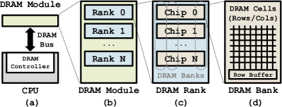
DRAM comprises a hierarchy of two-dimensional arrays, as shown in Figure 1. At the top level, a DRAM controller interfaces with a DRAM rank over a channel (Figure 1a). The channel conveys DRAM commands, addresses, and data between the DRAM controller and the DRAM rank. In modern systems, multiple DRAM ranks are typically combined in a DRAM module (Figure 1b). The DRAM controller uses chip-select signals to interface with only a single DRAM rank at any given time.
A DRAM rank consists of multiple physical DRAM chips (Figure 1c). The DRAM controller is unaware of how a single rank is partitioned into individual DRAM chips. Instead, it sees each rank as the union of multiple banks that are each striped across the physical DRAM chips that form the rank. Thus, one bank spans multiple DRAM chips, and a single DRAM chip stores data from multiple banks. This has implications on how failures affect banks. Different DRAM chips can have different failure profiles depending on how they are manufactured; thus, a “weak” DRAM chip affects multiple banks. However, only a portion of each bank is affected, namely, the portion that corresponds to the weak DRAM chip.
DRAM banks within a chip are further subdivided into rows and columns of storage cells (Figure 1d), where each cell encodes a single bit of data using the amount of charge stored in a capacitor (i.e., data “1” as either fully-charged or fully-discharged, and data “0” as its opposite). The DRAM controller accesses a cell by specifying a row address and a column address to a particular bank. It has no knowledge of the physical layout of banks or that a bank comprises multiple physical chips.
II-B How DRAM Operates
A DRAM read operation senses the amount of charge stored in cell capacitors. It is subdivided into three phases: (1) Activation (ACT): the charge stored in an entire DRAM row’s cells within a bank is sensed and stored in a row buffer. The row buffer acts as a fast cache; subsequent accesses to the same row do not require another activation. Instead, data is read out of the row buffer. (2) Read (RD): the contents of the row buffer at a given column address are returned to the DRAM controller. (3) Precharge (PRE): the bank is prepared for the next access by disconnecting and clearing the active row buffer.
All rows in a bank share one row buffer. Within a bank, the DRAM controller activates and reads from only one row at a time. Write operations work similarly to reads.
Refresh (REF): DRAM cells leak their charge, which can cause data loss when cells are not accessed frequently enough. To prevent this, the DRAM controller issues periodic refresh operations that replenish the cells’ charge. The DDR4 standard specifies that 8192 refresh commands be issued during a 64 ms time period [61], which results in considerable power consumption and performance overhead [85].
II-C The Rowhammer Threat
Modern deeply-scaled DRAM devices are susceptible to Rowhammer – a circuit-level disturbance phenomenon in which repeatedly activating and precharging a given row accelerates charge leakage in the storage cells of physically nearby rows [69]. With enough activate/precharge cycles, this phenomenon causes bit flips.
Prior work extensively studied the statistical characteristics of Rowhammer-susceptible storage cells [69, 92, 77, 91] and found that the magnitude of the error rate depends significantly on the number of activate/precharge cycles. Other factors affecting the error rates include the particular device under test, the ambient temperature, and the data pattern written into the cells. Recent work [115] identified the precise charge leakage path responsible for Rowhammer errors and provided a detailed model that explains experimental observations made by previous work [92].
Proposals for mitigating and/or preventing Rowhammer errors abound in both academia [5, 67, 102, 14, 56, 104, 29, 111, 80, 15, 7, 6, 9, 8, 34, 74, 58, 30, 63, 73, 99, 112] and industry [4, 39, 82, 24]; see [89] for a detailed survey of these works. However, while DRAM manufacturers claim that modern DRAM devices are resilient to Rowhammer bit-flips [81, 33], it is unclear what causes this resilience and under what conditions the Rowhammer-prevention mechanism may fail. Furthermore, even if a particular DRAM device is supposedly protected, there is no known way to verify that it is in fact fully resistant to Rowhammer bit flips.
II-D Intel-based Cloud Server Architectures
For the cloud market, Intel offers the scalable-performance variant of Xeon processors (often referred to as Xeon-SP). SP indicates a server class CPU for multi-socket cloud motherboards, introduced with Intel Skylake. Intel Broadwell uses EP to designate multi-socket server CPUs.
We performed our experiments on the three most recent generations of Xeon servers: Broadwell-EP, Skylake-SP, and Cascade Lake-SP. Skylake is a major architectural revision of Broadwell. Some of our results are affected by these architectural differences, such as whether the architecture supports the clflushopt instruction. Cascade Lake is a minor revision of Skylake, and, indeed, our results are similar on both of these platforms. Intel announced the upcoming release of Ice Lake-SP, a major architectural revision of Skylake, but these CPUs are not available at this time.
III Challenges of DRAM Testing
Previous work established a direct relationship between the number of DRAM row activations within back-to-back refresh (REF) commands and the number of observed bit flips. A good example is Figure 2 in a recent paper [89]. This observation is not new; it goes back to the original paper showing DRAM disturbance errors [69]. To test a DRAM row for its susceptibility to Rowhammer attacks, we repeatedly activate two adjacent rows co-located in the same bank. Alternating accesses to two rows ensures that each access first precharges the open row and then activates the row being accessed. We refer to the rows we activate as aggressor rows, and the tested row as the victim row.
Naively, to mount Rowhammer, one would like to activate only a single row repeatedly. Unfortunately, there is no way to accomplish this in practice on systems using an open-page policy [65] (the terms page and row are equivalent in this context). According to this policy, the memory controller leaves a DRAM row open in the row buffer after access. Accessing the same row leads to reading repeatedly from the bank’s row buffer rather than to multiple row activations. Open-page policy is the default configuration in most systems today, including the servers used by our cloud provider.
III-A Fundamental Testing Requirements
To identify all possible Rowhammer failures when a system is operational, our testing methodology must replicate the worst-case Rowhammer testing conditions. We identify two fundamental testing requirements: (1) The methodology must activate DRAM rows at the highest possible rate. Repeatedly activating a row toggles the wordline’s voltage, which causes disturbance errors. The testing methodology must toggle the wordline voltage at the fastest (i.e., worst-case) rate possible to ensure the largest number of wordline activations within a refresh interval. (2) The methodology must test each row by identifying and toggling physically adjacent rows within DRAM. Rowhammer attacks are most effective when aggressor rows are physically adjacent to the victim row [69]. Hammering rows without precise knowledge of physical adjacency is not an effective testing methodology.
III-B Challenges of Generating the Highest Rate of ACT Commands
The initial study of DRAM disturbance errors [69] directly attached DRAM modules to an FPGA board that acts as the memory controller and can issue arbitrary DRAM commands [38, 103]. The FPGA was programmed to issue ACT commands at the optimal rate determined by the DRAM timing parameter tRC (i.e., minimum row cycle time) in the JEDEC specification sheet [60, 61].
In contrast, testing DRAM on a cloud server is challenging due to the complexity of modern machines. Instruction sequences execute out-of-order, their memory accesses interact with a complex cache hierarchy designed to capture and exploit locality, and memory controllers implement complex DRAM access scheduling algorithms [90, 109]. To comprehensively test a cloud server for Rowhammer-vulnerable DRAM devices, we need to find the optimal instruction sequence that, when executed, causes the memory controller to issue ACT commands at the optimal rate (every tRC time interval).
Previous work on Rowhammer used a variety of different instruction sequences to mount the attack [69, 101, 32, 114, 13, 96, 11, 12, 37, 94, 97, 110, 77, 59, 2, 35, 36, 105, 25, 106, 83, 95, 16, 18, 10, 118, 22]. It is unclear whether these sequences lead to different rates of ACT commands, which sequence is the most effective, and how far from the optimal ACT rate each sequence is. Most previous work evaluated the effectiveness of an instruction sequence mounting a Rowhammer attack via the number of flipped bits metric. Unfortunately, this metric is inadequate for testing DRAM because it fails to distinguish a case where memory is safe from the case where the instruction sequence is ineffective.
III-C Challenges of Determining Adjacency of Rows Inside a DRAM Device
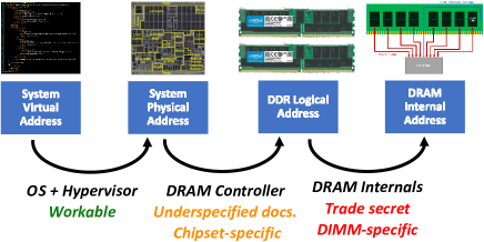
Instruction sequences access memory via virtual addresses. Virtual addresses are subject to at least three different remappings until mapped to an internal set of cells inside a DRAM device. Figure 2 shows the three different remapping layers.
1. Virtual-to-Physical: An OS maintains the map of virtual to physical addresses. A virtual address gets translated into a physical address by the CPU’s Memory Management Unit (MMU). Virtualized cloud servers have an additional mapping layer due to virtualization – virtual addresses are first remapped to guest-physical addresses, which are then remapped to host physical addresses.
2. Physical-to-Logical: A memory controller maintains a map (or mapping function) of physical addresses to DDR logical addresses (also called linear memory addresses [105]) and translates incoming physical addresses to DDR logical addresses. These DDR addresses are specified in terms of channel, DIMM, rank, bank, row, and column. These maps, seldom public, differ from one CPU architecture to another, and they are subject to various BIOS settings, such as interleaved memory [70]. On Skylake [42] and Broadwell [41], different memory controller configurations (e.g., page policies) [28] change these maps.
3. Logical-to-Internal: Vendors remap logical addresses in order to decrease the complexity of internal circuitry and PCB traces because some maps are electrically easier to build than others [84, 78, 66]. Remapping also lets vendors take advantage of the fact that DRAM devices have redundancy to tolerate a small number of faults per chip; vendors test for these faulty elements post packaging and remap wordlines or bitlines to redundant ones elsewhere in the array (i.e., post package repair) [26, 84]. Memory vendors regard these maps as trade secrets.
| Side-channels | Reduced timings | Heaters | Physical probing | Rowhammer attacks | |
|---|---|---|---|---|---|
| [100, 94] | [78, 68] | [64] | [100, 94] | [100, 94, 105] | |
| Fine-grained | ✖ | ✖ | ✖ | ✔ | ✔ |
| Non-invasive | ✔ | ✔ | ✖ | ✔ | ✔ |
| Finds Internal DRAM addresses | ✔ | ✔ | ✔ | ✖ | ✔ |
| Consistent | ✔ | ✔ | ✔ | ✔ | ✖ |
Previous work used a combination of side-channel attacks, reduced timing parameters, thermal heaters, physical probing, and Rowhammer attacks to reverse engineer parts of these maps [100, 94, 78, 64, 105]. Unfortunately, such techniques have shortcomings that prevent our methodology from using them. They are either too coarse-grained [100, 94, 78, 64], invasive (i.e., potentially damaging the chips) [64], inconsistent [100, 94, 105], or they do not capture DRAM internal addresses [100, 94].
Side-channel attacks are coarse-grained. All memory accesses to a DRAM bank share one row buffer. Prior work measured two addresses’ access times to determine whether they are co-located in the same bank [100, 94]. Sequentially accessing any two rows within the same bank takes longer than accessing two rows located in different banks. However, this method cannot provide finer-grained adjacency information. The time spent accessing two rows sequentially in the same bank is unrelated to the rows’ locations within the bank.
Reduced timing parameters is coarse-grained. Another technique uses the distance from a row to the bank’s row buffer [78, 68]. This technique induces errors by accessing memory using shorter-than-normal DDR timing values. Data stored in a cell closer to the row buffer has a shorter distance to travel than data stored further away [79], and thus, it has a lower likelihood to fail. This technique provides coarse-grained and approximate row adjacency information only. Adjacent rows have a negligible difference in access times, and detecting such small differences is challenging.
Using heaters is invasive and coarse-grained. Another technique surrounds a DIMM with resistive heaters, applies a thermal gradient on each DRAM device, and conducts a retention error analysis [64]. This approach requires high temperatures, in excess of C. Cloud providers are reluctant to adopt a testing methodology that heats up their hardware. Also, the thermal gradient approach is coarse-grained; it can only determine neighborhood relations rather than row adjacency.
Physical probing does not capture DRAM internal addresses. Another approach uses an oscilloscope probe to capture a DDR electrical signal while issuing memory accesses [100, 94]. This approach cannot reverse engineer how DDR logical addresses map to DRAM internal addresses (Figure 2). Previous work used this technique to reverse engineer only bank addresses [100, 94]. Reverse engineering row addresses would incur significant additional effort for two reasons. First, row addresses require 22 individual probes, whereas bank addresses require only 4 probes. Second, the signals encoding row addresses change from one DDR4 command to another (Table II). The reverse engineering effort would need to ensure that the probes capture only the signals encoding DDR4 row activation, and not other commands. In contrast, signals encoding bank addresses are shared by DDR4 row activation, read, write, and precharge commands. Capturing the signals corresponding to any one of these DDR4 commands reveals the bank address.
Rowhammer attacks are not consistent because they may not cause failures. Another technique mounts Rowhammer attacks on every row in DRAM and correlates each row’s density of bit flips with adjacency [100, 94, 105]. Generating a high rate of activations is enough to cause many bit flips on some DIMMs, but not on all. This approach is unsuitable for testing memory resilient to Rowhammer. This is an instance of a chicken-and-egg problem: (1) testing DRAM for Rowhammer susceptibility requires knowing the adjacency of rows inside DRAM devices, and (2) deducing row adjacency requires flipping bits using Rowhammer attacks.
Table I summarizes the limitations of previous work on reverse engineering row adjacency inside DRAM.
IV Step 1: Generating the Highest Rate of ACT Commands on a Server Architecture
We first describe the system setup we used to measure the rate of row activations of an instruction sequence. Measuring ACT rates lets us (1) find which instruction sequence generates the highest ACT rate on a particular server platform, and (2) quantify the difference between this highest ACT rate and the optimal rate determined from DRAM datasheets [61]. We then evaluate the performance of instruction sequences used by prior work to mount Rowhammer. Finally, we present a new instruction sequence that generates near-optimal row activation rates on Intel Skylake and Cascade Lake architectures.
IV-A System Setup for Measuring ACT Rates
To determine the instruction sequence that generates the highest rate of ACT commands, we used the FS2800 DDR Detective from FuturePlus Systems with two DIMM interposers for DDR3 and DDR4 [27]. This system can monitor, capture, and measure DDR commands issued over the command bus to the DIMM using a DDR interposer and an FPGA that triggers on specific DDR commands or memory addresses. Once triggered, the FPGA records all DDR commands it observes on the bus and stores them in buffers, which are later transferred to a host computer over USB.
The traces gathered with the bus analyzer provide ground truth information about the rate of activations of a DRAM row and the memory controller’s behavior, including the logical addresses used to access DRAM. We use these traces to characterize the ACT rates of different Rowhammer instruction sequences from previous work and to construct a sequence that has a near-optimal ACT rate on Skylake and Cascade Lake.
We found it difficult to use a high-level OS (e.g., Linux) for our methodology for two reasons: (1) an OS introduces complex virtual-to-physical address mappings that can change dynamically, and (2) an OS’s services introduce interfering traffic to a DIMM when testing.
Instead, our methodology boots the computer into the UEFI mode [107]. In this mode, the virtual-to-physical address map is linear and does not change across reboots. UEFI’s simplicity and lack of OS services eliminate any interfering DDR traffic from our traces. However, it also increases the amount of engineering effort required to implement our testing methodology because UEFI lacks many services commonly found in a commodity OS. Therefore, we had to implement support for multi-threading, hardware discovery [108, 19] and performance counters.
IV-B Performance Evaluation of Prior Instruction Sequences
Our results are based on experiments with six server-class DIMMs that one cloud provider sourced from three different memory vendors, two DIMMs per vendor. In alphabetical order, these vendors are: Hynix, Micron, and Samsung. Although sourced from different vendors, the DIMMs’ specs are similar; they are registered ECC 32GB DDR4 (x4); the DIMMs from two of the vendors have transfer rates of 2400 MT/s; and the third vendor’s DIMMs have rates of 2666 MT/s. We found negligible differences in the performance of an instruction sequence from one DIMM to another. For consistency, the results presented in this section use the same DIMM. One of the timing parameters in the JEDEC specification is row cycle time (tRC) – the minimum period of time between two back-to-back ACT commands. The JEDEC specification lists tables of minimum and maximum tRC values for different types of DDR4 memory; these values depend on many memory characteristics, such as speed, clock cycle, capacity, and so on. Based on our DDR4 memory’s characteristics, the JEDEC specification lists the minimum value of tRC as 47ns and does not specify a maximum value (see Table 110 in [61]).
We measured tRC to be 46.7ns on all our hardware, corresponding to a rate of 167.4 ACT commands between two consecutive REF commands issued by the memory controller (i.e., one tREFI interval in JEDEC terminology). We call 46.7ns the optimal latency between two ACT commands, and 167.4 ACTs/tREFI the optimal rate. All results presented are based on experiments running on Skylake, although we ran many of these experiments on Broadwell and Cascade Lake with similar results. All servers use motherboards with multiple CPU sockets.
Previous work used a variety of different instruction sequences in a loop to test for Rowhammer [69, 32, 114, 13, 96, 11, 37, 94, 97, 110, 77, 59, 2, 35, 36, 105]. Some of these sequences use memory barriers to serialize the memory accesses on each iteration of the loop [69, 114, 96, 59], whereas others do not [32, 114, 11, 94, 37, 110, 2, 105]. To bypass the cache hierarchy, some instruction sequences use an explicit CPU flush instruction (e.g., clflush), but not all do. Some use cache collisions to flush the cache [83]; others hypothesize that non-temporal load instructions [44] could bypass the cache [110, 35]. Another strategy we encountered was choosing a pair of rows to hammer from a memory region marked as uncached [35]. Finally, the x86-64 architecture offers additional instructions for cache invalidation, such as invd [45] and wbinvd [46].
The pseudo-code in Figure 3 describes a typical sequence that issues two load instructions, two clflush instructions, and a global memory barrier, all in one loop. Several papers on Rowhammer [69, 114, 96], including the original Rowhammer work [69], used this sequence.
Faced with all these choices of possible instruction sequences, we considered two questions: (1) Which prior instruction sequence maximizes the rate of ACT commands? (2) How far from the optimal rate of ACT commands is the best instruction sequence?
To answer these questions, we constructed 42 different instruction sequences that let us experiment with:
All three types of fences available on x86-64 architectures: mfence [47], lfence [48], and sfence [49].
Both clflush and clflushopt [50] commands (the latter is an optimized cache flushing command with weaker ordering semantics than the former).
Marking as uncacheable the hammered memory pages’ PTEs, which eliminates the need to issue any CPU flush commands.
Both regular and non-temporal [44] memory accesses.
Using a cache invalidation scheme based on cache line conflicts, similar to the one used by Nethammer [83] and ANVIL [5].
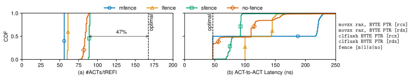
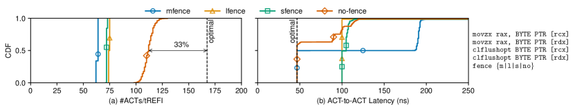
Figure 4 shows the performance of four typical instruction sequences used in many previous Rowhammer attack papers [69, 32, 114, 11, 94, 37, 110, 96, 2, 105]. These four sequences are identical except for the type of memory barrier they use to serialize the reads and flushes on each loop iteration. The assembly code is shown to the right of the graphs; the four sequences use mfence [47], lfence [48], sfence [49], and no fence at all, respectively.
Figure 4a shows the CDF of the rate of row activations for each sequence as well as the optimal rate (with a dashed line). Despite the popularity of these instruction sequences, which were used by previous papers to mount Rowhammer attacks, we discovered that they do not create worst-case ACT rates – their rates of row activations are 47% from optimal. Even worse, using mfence, a sequence used by [69, 114, 96], leads to the slowest ACT rate of the four sequences. The most effective sequences impose no ordering and use no fences or only store fences (sfence). A store fence has no ordering effect because no sequences issue any stores.
Figure 4b shows the CDF of the latencies between two consecutive row activations for each instruction sequence. Although the sequence using mfence has the slowest ACT rate, half of its latencies are optimal. We examined its behavior closely and found that the two reads inside the loop are always issued back-to-back at the optimal latency (46.7ns). However, the next ACT command is issued after a long delay of over 220ns, which is caused by the mfence. The delay explains why this sequence has a low rate of ACT commands This bimodal delay between ACTs is clearly visible in Figure 4b.
These results illustrate the gap between a proof-of-concept Rowhammer attack and the needs of a DRAM testing methodology. Although the instruction sequences shown in Figure 4 have been used in many papers to mount various successful Rowhammer attacks, their ACT rates are far from optimal. This suggests that the DIMMs found vulnerable in previous work succumbed even to a low-rate Rowhammer attack. A DRAM testing methodology based on these instruction sequences falls short of creating the worst-case testing conditions for DRAM, which is necessary to confidently determine whether a chip is vulnerable to Rowhammer.
Using clflushopt improves ACT rates. With Skylake, Intel introduced an optimized version of the cache flush instruction, called clflushopt, that has weaker ordering requirements than clflush [50, 54]. Multiple clflushopt instructions to different cache lines can execute in parallel. We performed a detailed analysis by implementing support for performance counters in UEFI mode [107]. We found that using clflushopt in our instruction sequences takes only 3 micro-ops, whereas clflush takes 4.
Figure 5 shows the three instruction sequences using memory barriers that have similar ACT rates; some have slightly higher rates (the ones using sfence and lfence), whereas others have slightly lower rates (the one using mfence). Although it is difficult to quantify how different types of barriers affect the performance of the two cache line flush instructions, the high-level finding remains the same: memory barriers are slow, and instruction sequences using barriers have low ACT rates.
In contrast, the sequence that uses no memory barriers has a much higher rate of ACT commands of 112 every tREFI, corresponding to 33% from optimal. The lack of a memory barrier causes this instruction sequence to have the highest ACT rate overall. This finding is not intuitive – the lack of memory barriers makes the CPU re-order memory accesses to increase the likelihood that they will be served from the cache. We measured this sequence and found its cache hit rate to be 33% (in contrast, the sequence using mfence has a 0% cache hit rate). Despite the CPU cache acting as a de facto rate limiter to Rowhammer attacks, the ACT rate of this instruction sequence is higher than those using any type of barrier.
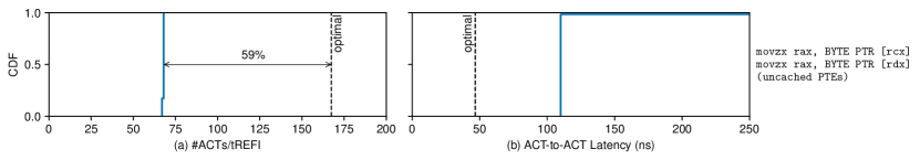
Uncached PTEs. We experimented with an instruction sequence that does not issue cache flushes, but instead marks its memory pages uncacheable. The sequence has a low rate of ACT commands.
Figure 6 shows the performance of an instruction sequence that does not issue cache flushes, but instead marks its memory pages uncacheable. Such a sequence has a low rate of ACT commands, and also a very regular behavior: its ACT-to-ACT latencies are almost always 110ns apart (in a small fraction of cases, this latency increases because the ACT is blocked behind an ongoing refresh command). These results suggest that loading an address from uncached memory has a fixed high cost, making this instruction sequence have a low rate of ACT commands.
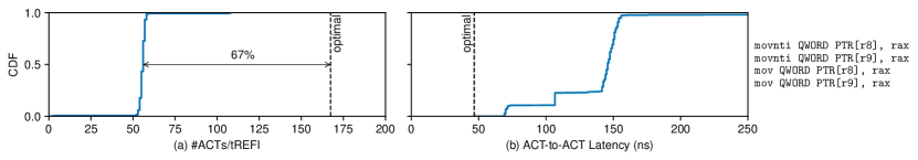
Non-temporal memory accesses. Intel offers five non-temporal store instructions for different data types (e.g., integers, doublewords, floating point, etc.) and one load instruction for double quadwords. These instructions do not follow normal cache-coherence rules and fetch their corresponding cache line from DRAM.
While experimenting with non-temporal instructions, we discovered that accesses are cached, and not served by DRAM. According to Intel’s documentation, these accesses use a form of temporary internal buffers that might prevent them from accessing DRAM, which can explain our findings.
We also experimented with instruction sequences that combine non-temporal and regular memory accesses. We expected that the different caching semantics of these two types of memory accesses would flush the caches (or internal buffers) in each loop iteration. Previous work also proposed mixing these two types of memory accesses for mounting Rowhammer [35]. We found these instruction sequences to be ineffective. Figure 7 shows the performance of one such instruction sequence to be far from optimal (67% from optimal).
Full cache invalidations, cache collisions, loads vs. stores. We experimented with replacing the cache line flush instructions with full cache invalidation instructions: invd [45] and wbinvd [46]. We found that full cache invalidation instructions are very expensive, making the instruction sequences have low ACT rates. We also experimented with generating cache conflicts to evict cache lines, but did not find higher ACT rates. Finally, we experimented with replacing loads with stores in various instruction sequences and found negligible performance differences. For brevity, we omit showing these results.
Differences across memory vendors. While all results shown use DRAM from one single vendor, we performed these experiments on DRAM from all three vendors. When using the same instruction sequence, we found no significant differences in the ACT rates when using DRAM from different vendors.
Key Takeaways
All previously proposed instruction sequences are sub-optimal for two reasons: (1) memory barriers are expensive and thus reduce the ACT rate, and (2) in the absence of memory barriers, the CPU re-orders memory accesses to increase the cache hit rate and avoid accessing DRAM.
Using uncached PTEs or non-temporal instructions is ineffective, leading to negligible changes to ACT rates when compared to the more common Rowhammer instruction sequences.
The most effective instruction sequence proposed in previous works uses two load, two clflushopt instructions, and no memory barriers at 33% from the optimal rate (Figure 5).
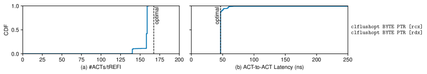
IV-C clflushopt Alone Hammers Near-Optimally on Skylake and Cascade Lake
To increase the rate of ACT commands, we experimented with new instruction sequences that (1) do not use memory barriers, and (2) are less prone to the effects of out-of-order execution. Our experiments revealed that a cache line flush instruction results in a memory access.
Figure 8 characterizes the rate of ACT commands of a sequence consisting of two clflushopt instructions in a loop; (these results are from our experiments on the Skylake-based server, but they are very similar to those performed on Cascade Lake). Figure 8b shows that over 87% of ACTs are issued at the optimal rate, about 46.7ns apart from one another. The remaining 13% are separated by an additional 10-20ns due to conflicts with ongoing refresh commands (REF). When the memory controller issues a REF, the bank remains inaccessible until the REF finishes [17], and any ongoing ACT is blocked waiting for the REF to finish. The REF-induced delay causes this instruction sequence to issue 159 row activations for every tREFI, a rate we call near-optimal.
The microarchitectural side-effects of clflushopt causes this instruction sequence to issue row activations at a rate that is 44% higher than the best previously known Rowhammer sequence (159 vs 110 ACTs/tREFI). It is unlikely another sequence could improve this rate because row activations will still conflict with REFs that block the bank. Two clflushopt instructions in a loop thus create the worst-case DRAM “hammering” conditions on Skylake and Cascade Lake.
Why does clflushopt cause memory accesses? This instruction sequence is highly surprising in the context of a Rowhammer attack because it uses no explicit memory accesses. Instead, the memory access (a DDR4 read operation) is a microarchitectural side-effect of the CPU executing a cache line flush. It occurs only when the cache line is invalid. Issuing a cache line flush instruction to a line present in the cache does not cause any DDR read operations.
Our instruction sequence (Figure 8) causes two memory accesses for each loop iteration except for the first iteration. The first loop iteration does not generate memory accesses when the lines are in the cache. However, it invalidates the cache lines, causing all subsequent iterations to generate two memory accesses.
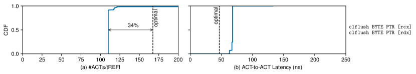
According to Intel’s specification [52, 86], systems with multiple processors may maintain cache coherence state of each cache line within the line itself in memory. When executing clflushopt on an invalid cache line, the processor reads cache directory state from DRAM to determine whether the line is present in other processors’ caches. We verified clflushopt’s behavior on both Cascade Lake and Skylake. We also show that clflush behaves similarly on both Cascade Lake and Skylake, but on Broadwell clflush results in no memory accesses. We hypothesize that clflush has more system overhead than clflushopt because it is subject to additional ordering constraints [51], leading to a reduced rate of DRAM row activations. Figure 9 shows the performance of a sequence using two clflush instructions in a loop; it activates rows at a rate of 110 every tREFI, corresponding to 65.7% of optimal.
V Step 2: Reverse Engineering Row Adjacency in Any DRAM Device
No technique used in previous work is suitable for reverse engineering row adjacency: some are not fine-grained and cannot determine adjacency at the level of an individual row [100, 94, 78, 64], whereas others do not capture addresses internal to DRAM devices and thus can determine adjacency only in the DDR4 bus address space [100, 94]. The single previous technique that can overcome these limitations works only if the device succumbs to Rowhammer attacks [100, 94, 105]. Section III-C describes these techniques and their trade-offs in depth.
In an attempt to guarantee Rowhammer failures on our DRAM devices, we experimented with lowering the refresh rates of our servers. A low refresh rate ensures that an attack sends a higher number of ACT commands to a victim row before the row can refresh. This increases the attack’s likelihood of success. Unfortunately, our experiments were unsuccessful. Recent hardware makes it increasingly difficult to set the refresh rates sufficiently low to successfully mount a Rowhammer attack. Older generation BIOSes running on DDR3-equipped hardware can set refresh rates up to 12x lower than normal; such low refresh rates make DDR3 devices succumb to Rowhammer attacks.
Modern BIOSes for DDR4 hardware restrict lowering the rate to only 3.5x. Unfortunately, this refresh rate is not sufficiently low to guarantee Rowhammer failures on our servers. We also confirmed this is not a GUI restriction: we examined the BIOS source code and found that the refresh interval configuration register cannot hold a value larger than one corresponding to a refresh rate of 3.5x lower.
V-A DDR4 Fault Injector
Because modern BIOSes restrict lowering the DRAM refresh rate, we used a different approach: we designed a DDR4 fault injector that blocks REFs sent by a memory controller to an individual DIMM. Our fault injector manipulates electrical signals and drives them from low to high, and vice-versa. Manipulating the DDR bus’s electrical signals effectively changes one DDR command into another. This insight was inspired by previous work that used a custom-made shunt probe to induce faults in DRAM data and thus reverse engineered the DRAM controller’s ECC scheme [18]. Figure 10 shows our fault injector, and Figure 11 shows its schematic.
Side-effects. Manipulating electrical signals to change DDR4 commands introduces side-effects. For example, changing a signal known as makes all DDR4 commands decode as row activate (ACT) commands. In this case, a DIMM becomes inaccessible because it receives only ACTs no matter what command the memory controller is issuing. Table II (reproduced from Wikipedia [113]) shows the encoding of DDR4 commands.
![[Uncaptioned image]](/html/2003.04498/assets/figs/ddr4.png)
Instead, we need to control these side-effects to leave the DIMM in a responsive state; otherwise, we cannot mount a Rowhammer attack. The DIMM must continue to receive row activates, row reads (or writes), and row precharges.
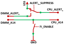
Overcoming the side-effects. Our fault injector changes the A14 signal from high to low and turns REF commands into a different DDR command, known as mode register (MR0) [61] with a null payload. Although this new command affects the DIMM’s configuration, the DIMM continues to serve all incoming commands. We designed our fault injector to trigger memory recalibration and thus reset the DIMM’s configuration back to its original settings.
Manipulating the A14 signal has an additional side-effect: it changes a read into a write command (see [113]). To overcome this side-effect, our Rowhammer attack instruction sequence uses stores rather than loads. Fortunately, manipulating the A14 signal does not affect the row activations and precharges needed to mount a Rowhammer attack.
Memory recalibration. The memory controller performs memory recalibration upon detecting an error. One such error is a parity check failure for DDR4 signals. On an incoming command, the DIMM checks parity, and, if the check fails, it alerts the memory controller through a reverse signal called . Upon receiving the alert, the memory controller sends a sequence of DDR recalibration commands to the DIMM.
We designed our fault injector to also recalibrate memory, but only when the Rowhammer attack completes. This restores the DIMM to its original configuration and lets us inspect the location of the bit flips that could reverse engineer row adjacency in the DRAM device. Memory recalibration cannot occur during an ongoing Rowhammer attack because it creates interference.
To recalibrate memory, our fault injector also manipulates the signal. During an ongoing Rowhammer attack, it suppresses the signal, thus preventing the memory controller from receiving any alerts. Once the attack completes, the fault injector re-enables while continuing to manipulate A14 to ensure that parity checks continue to fail. These alerts are now received by the memory controller, which, in turn, recalibrates the DIMM.
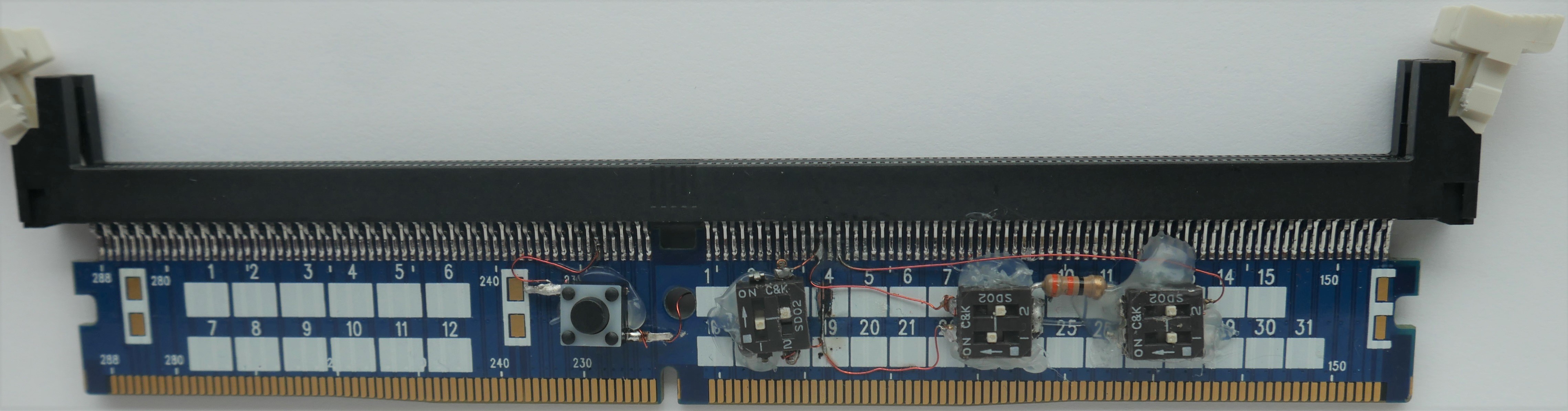
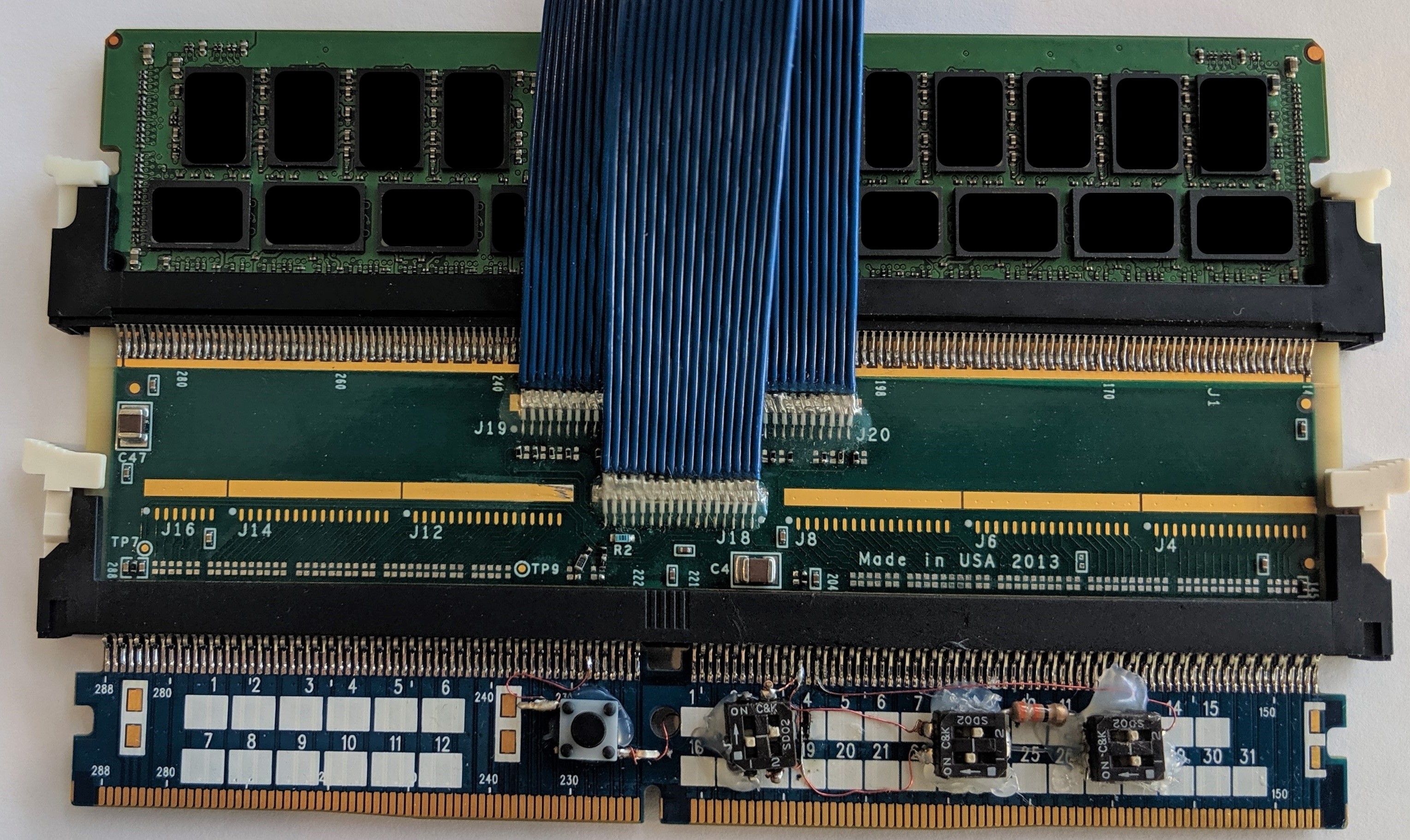
Methodology for injecting DDR4 faults. Figure 12 shows our hardware stack: the fault injector, the bus analyzer’s interposer, and the DDR4 DIMM. We used an eight-step operational plan to inject faults and mount Rowhammer to induce bit flips capable of reverse engineering row adjacency:
1. Boot server with DDR parity check enabled and ECC disabled.
2. Suppress signal with DIP switches.
3. Begin Rowhammering the target DIMM.
4. Inject a fault in the A14 signal by pressing the button switch for a fixed time interval. During this time, the DIMM receives no REFs, and the memory controller receives no alerts.
5. Stop Rowhammering the target DIMM.
6. Re-connect signal with DIP switches.
7. Inject a fault in the A14 signal by tapping the button. The memory controller receives alerts from the DIMM and starts recalibrating the DIMM.
8. Inspect the number and spatial distribution of bit flips.
V-B Row Adjacency in DRAM Devices
We used the fault injector to reverse engineer the physical row adjacency of DRAM devices mounted on DDR4 DIMMs. We mounted Rowhammer attacks and measured the density of bit flips across each row within a bank. This technique correlates each row’s density of bit flips with adjacency [100, 94, 105]. Invariably, when hammering one row for 15 seconds without refreshes, a small number of rows flip bits at a much higher rate than all others. This indicates that these highly affected rows are physically adjacent to the hammered one.
We then posed the following questions:
1. Do logical addresses map linearly to internal DRAM addresses? A linear map makes it easier to mount Rowhammer because an attacker need not reverse engineer it. Previous work showed that the map from physical to logical addresses is not linear and discussed how non-linearity can render many of the Rowhammer defenses much less effective than initially thought [105].
2. Does the position of a bit within a word influence its likelihood of being flipped? Such results would shed light on whether some words (or some bits within a single word) are more susceptible to Rowhammer attacks than others. For example, most page table entries have a format in which low-order bits control access to a page; should the low-order bits be more susceptible than high-order, an attack changing the access control policy to a page would be more likely to succeed.
3. How do data patterns affect the susceptibility of bits being flipped? We examined the direction in which bits flip (0-to-1 or 1-to-0). The memory controllers in datacenter servers are routinely configured to scramble data in DRAM by xor-ing it with a known, random data pattern [87, 43]. This means that the proportion of 0s to 1s in DRAM is 50-50.
4. Do DIMMs sourced from different vendors have different characteristics? We examined whether or not the map and the rate at which bits flip are consistent across DIMMs from different vendors.
Methodology. We performed all experiments by suppressing REFs for 15 seconds at room temperature. We disabled data scrambling and wrote a specific data pattern across the entire bank except for the hammered row. We wrote the complement of the data pattern in the hammered row, a strategy used by previous work [62]. We experimented with four different data patterns that vary the locations and ratios of bits set to 1 vs. bits set to 0. The four patterns are: all 1s, 0xB6DB6DB… (corresponding to two-thirds 1s), 0x492492… (corresponding to one-third 1s), and all 0s. Unless marked otherwise, the results we present use a pattern of all 1s.
When testing DRAM, a double-sided Rowhammer attack (i.e., two aggressor rows) is better than single-sided (i.e., one aggressor row). However, when injecting faults, both types of Rowhammer attack flip bits because the DIMM does not refresh for 15 seconds. When reverse engineering row adjacency, single-sided Rowhammer is simpler because the adjacency of a flipped bit is unambiguous – it is due to a single aggressor. Reverse engineering row adjacency with double-sided Rowhammer leads to an attribution challenge – is the flipped bit adjacent to aggressor #1 or aggressor #2? The results in this section are based on using a single aggressor row, similar to mounting a single-sided Rowhammer attack.
Our results show no differences between the DIMMs from the same memory vendor. Most results are similar across DIMMs supplied by different vendors; in these cases, we present the results from a single vendor (referred to as vendor #1). However, we note different vendors in the text when results differ across vendors.
We verified that our fault injector suppresses refreshes on all three Intel server architectures. We also reverse engineered portions of the row adjacency maps of three DIMMs (one from each vendor) on both Broadwell and Skylake and checked that the results are identical on both platforms. On Cascade Lake, we reverse engineered only one DIMM, with identical results to Broadwell and Skylake. The data shown in the remainder of this section was gathered on the Skylake platform.
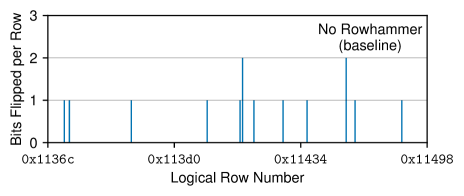
Results. We started with a baseline experiment in which we suppressed REFs for 15 seconds without any additional memory workload. Our goal was to determine the rate of bit flips due solely to suppressing REFs. These bit flips are not correlated with physical row adjacency. If we observed many such bit flips, combining suppressing REFs with Rowhammer attacks would make it difficult to attribute responsibility for the bit flips.
Fortunately, Figure 13 shows that the number of flipped bits is low. Even after suppressing REFs for 15 seconds, the majority of rows show no failures. Ten rows have a single flipped bit (a row failure rate of 3.3%), and two have two flipped bits (a row failure rate of 0.7%). No row has more than two flipped bits. The low number of failures demonstrates that our DRAM is resilient when not refreshed in the absence of Rowhammer attacks.
| Aggressor | Victim #1 | Victim #2 | Victim #3 |
|---|---|---|---|
| 0x11408 | 0x11409 (75.7%) | 0x11407 (40.0%) | 0x11417 (36.7%) |
| 0x11409 | 0x11408 (76.6%) | 0x1140A (76.5%) | |
| 0x1140A | 0x11409 (75.3%) | 0x1140B (74.2%) | |
| 0x1140B | 0x1140C (80.3%) | 0x1140A (79.5%) | |
| 0x1140C | 0x1140B (77.0%) | 0x1140D (76.5%) | |
| 0x1140D | 0x1140C (76.6%) | 0x1140E (75.9%) | |
| 0x1140E | 0x1140D (77.5%) | 0x1140F (76.6%) | |
| 0x1140F | 0x1140E (77.5%) | 0x11410 (39.9%) | 0x11400 (37.7%) |
| 0x11410 | 0x11411 (77.7%) | 0x1140F (40.5%) | 0x1141F (37.7%) |
| 0x11411 | 0x11412 (77.0%) | 0x11410 (76.7%) | |
| 0x11412 | 0x11411 (78.1%) | 0x11413 (77.2%) | |
| 0x11413 | 0x11414 (77.1%) | 0x11412 (76.4%) | |
| 0x11414 | 0x11413 (74.7%) | 0x11415 (74.0%) | |
| 0x11415 | 0x11414 (77.8%) | 0x11416 (77.4%) | |
| 0x11416 | 0x11415 (79.1%) | 0x11417 (78.3%) | |
| 0x11417 | 0x11416 (75.8%) | 0x11418 (39.4%) | 0x11408 (36.8%) |
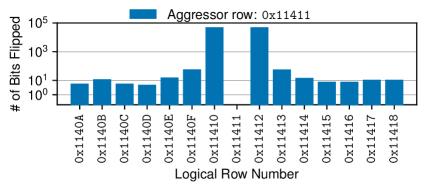
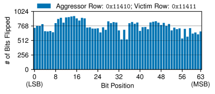
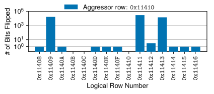
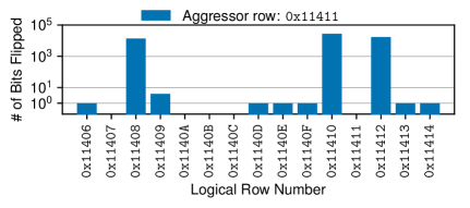
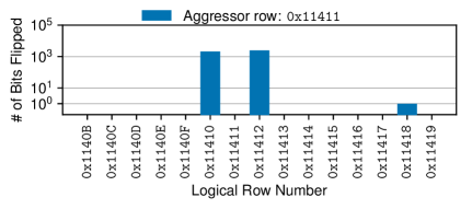
Logical rows do not always map linearly. Figure 14a shows the number of flipped bits per row when the aggressor was row 0x11411 (logical address). The results suggest a linear map because most bit flips occur on rows 0x11410 and 0x11412 (the y-axis is logarithmic). Row 0x11410 has 50,274 flipped bits (out of 65536, or 76.7%), and row 0x11412 has 50,489 (77.0%). All other rows have significantly fewer flipped bits.
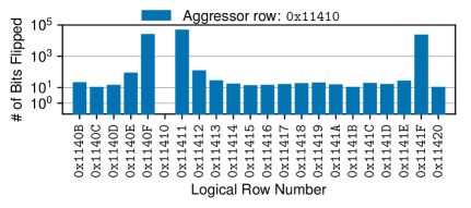
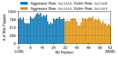
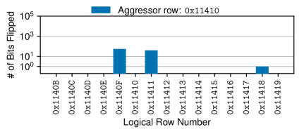
However, the map is not always linear. Figure 14b shows the results when the aggressor row address was 0x11410. While victim row 0x11411 is adjacent (with over 77% of its flipped bits), victim row 0x1140F, although adjacent in the logical address space, has only 26,566 flipped bits corresponding to 40.5% of its bits. Instead, a third victim row (0x1141F) has 24,680 of its flipped bits (37.7%). These results indicate that the aggressor row 0x11410 is adjacent to half of victim rows 0x1140F and 0x1141F. For brevity, we say a victim has whole-row (or half-row) adjacency to refer to the adjacency of the victim to the aggressor row.
Table III presents the row adjacency map inside the DRAM device for 16 consecutive rows in the logical address space. We conducted 16 experiments in which a different row acts as the aggressor, and list the top two or three victim rows sorted by the fraction of their bits that flip (shown in parentheses); all remaining victims have fewer than 1% of their bits flip. The data shows bimodal behavior: many rows map linearly (whole-row adjacency), but some have each of their halves mapped differently (half-row adjacency). Half-row adjacency in shown in bold in Table III.
When examining different portions of the adjacency map, we found that half-rows occur frequently but lack a specific pattern. Table IV shows the adjacency map for the first rows of the bank. Row 0 is half-adjacent to row F, but the remaining half is not adjacent to any other row in the bank. Half of row 0 is located either next to a spare row [40] or on the physical edge of the DRAM array. Also, some rows shown in Table IV have an adjacency pattern different from all others. For example, row 7 is half adjacent to rows 8 and 0x07f8.
| Row | Adjacent Rows | ||
|---|---|---|---|
| 0x0000 | 0x0001 (W) | 0x000F (H) | spare row/bank edge (?) |
| 0x0001 | 0x0000 (W) | 0x0002 (W) | |
| 0x0002 | 0x0001 (W) | 0x0003 (W) | |
| 0x0003 | 0x0002 (W) | 0x0004 (W) | |
| 0x0004 | 0x0003 (W) | 0x0005 (W) | |
| 0x0005 | 0x0004 (W) | 0x0006 (W) | |
| 0x0006 | 0x0005 (W) | 0x0007 (W) | |
| 0x0007 | 0x0006 (W) | 0x0008 (H) | 0x07F8 (H) |
| 0x0008 | 0x0009 (W) | 0x0007 (H) | 0x0017 (H) |
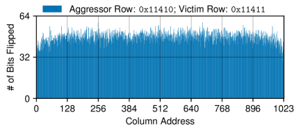
Fewer bits flip in half-rows than in whole-rows. We characterize whether a bit’s position influences its likelihood to be flipped. We start by grouping bit flips in a victim row by their column addresses (a column address specifies a word). A row has 1024 columns, and a column contains a 64-bit word.
Figure 15a shows data from a whole-row victim. Although some words have more bit flips than others, this variation is relatively low: more than 95% of all words have 40 to 60 bit flips, and a word has 47.6 bit flips on average. This result suggests that an aggressor row affects all words in a victim whole-row more or less equally.
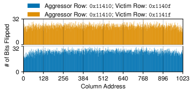
Half-row victims have half the number of bit flips per word (the remaining non-adjacent half is safe). Figure 15b shows the number of bit flips per word found in two half-row victims. Each word has 25 and 23 bit flips, respectively, on average as opposed to 47.6 bit flips for words located in a whole-row. This result suggests that an aggressor row affects fewer bits per word in victim half-rows than victim whole-rows.
All bits are equally susceptible for whole-row, but not for half-row, adjacency. We further investigated whether the position of a bit in a word affects its likelihood of being flipped? For this, we re-plotted the data from Figure 15 by grouping bits by their bit position rather than their column address. A row has 1024 bits in each bit position. Bit positions are indexed 0 to 63 from the least to the most significant bit.
Figure 16a shows the results of a whole-row victim. As before, an aggressor row affects all bits in a victim whole-row equally. Figure 16b shows the results for two half-row victims. Surprisingly, the sets of bit positions are disjoint. One of the half-row victims has bit flips in positions 0 through 31 only, whereas the other has bit flips in positions 32 through 63.
These results indicate that the position of a bit determines its likelihood of being flipped in half-rows only. In a victim half-row, either the most significant (63-32) or the least significant (31-0) bits are flipped, depending on memory geometry. For little endian systems (such as ours), the region containing bit flips will inversely map to the most or least significant bits, respectively. For example, in big endian systems, the map will be direct: words in row 0x1140F will have their least significant bits flipped, while words in row 0x1141F, their most significant. All DIMMs from all three hardware vendors exhibited this behavior.
Most, but not all, bits flip from 1 to 0. Electromagnetic coupling (considered to be a main reason for Rowhammer [69]) drains capacitors faster than normal. Memory encodings can represent a charged capacitor as either a 1 or a 0, making the data pattern another factor in a bit’s susceptibility to be flipped. Cells that encode data value 1 as a charge are called true-cells, while anti-cells encode data value 0 as a charge [75].
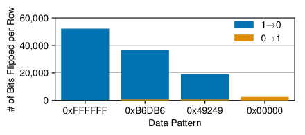
To examine this effect, we seeded memory with four data patterns: all 1s, two-thirds 1s (0xB6DB6D…), one-third 1s (0x492492…), and all 0s. Figure 17 shows the number of bit flips in a victim row for different data patterns. This number is directly proportional to the number of bits seeded with a value of 1: 79.7% for all 1s, 57% for two-thirds 1s, 29.9% for one-third 1s, and 3.8% for all 0s. While bits can flip in both directions, most bit flips were seeded with a value of 1.
DIMMs from vendors #2 and #3 have fewer bit flips. We repeated the experiments with DIMMs sourced from the other two hardware vendors. Vendor #2 has fewer bit flips per row than vendor #1. Figure 18 shows the number of bit flips for vendor #2 for the same aggressor rows as before: 0x11410 and 0x11411. When the aggressor row is 0x11410, the whole-row victim (0x11411) has only 42.1% of its bits flipped, while the half-row victims (0x11409 and 0x11413) have 25.9% and 21% of their bits flipped, respectively.
Further, the map differs from one vendor to another. Vendor #1’s row 0x11411 has two rows wholly adjacent, rows 0x11410 and 0x11412 (Figure 14). Instead, for vendor #2, this row has whole-row adjacency with row 0x11410 but only half-row with row 0x11412 and the other half with 0x11408.
Figure 19 shows that vendor #3 has far fewer bit flips than both other vendors. When the aggressor is row # 0x11410, the adjacent rows have only about 0.08% of their bits flipped (roughly two orders of magnitude fewer flips than vendor #1). When the aggressor is row # 0x11411, the adjacent rows have about 3% of their bits flipped (one order of magnitude fewer flips than vendor #1).
To understand whether the lower rate of bit flips for vendors #2 and #3 can be attributed to different encoding schemes, we repeated these experiments with a data pattern of all 0s. We found that even fewer bits flip. For all three vendors, most bits in victim rows flip when seeded with a value of 1.
In order to pinpoint the reasons why vendor #2 and #3’s DIMMs were more resilient than vendor #1’s DIMMs, we decoded the part numbers of each DIMM from each vendor, checking for differences in lithography. We found that each vendor used a different lithography process; vendor #1’s process had the highest density, vendor #2 had lower density, and vendor #3 had the lowest one. These results suggest that increasing DRAM density increases the probability of flipping bits in a Rowhammer attack. Previous work also found different rates of bit flips in different DIMMs [69, 105].
VI Operational Aspects of DRAM Testing Methodology
Our DRAM testing methodology uses two clflushopt instructions in a loop to hammer DRAM. For each row to test, we use address maps to identify adjacent rows. We seed the aggressor row with 0s and the victims with 1s. If the tested row has two adjacent full-rows, we find two virtual addresses that map to each of these rows, to seed our two cache line flush instructions. For each row, we run the test for 128ms, corresponding to twice the duration of a refresh interval. In this way, we ensure that our tests span at least one entire refresh interval. At the end of the test, we check whether the tested row has any of its bits flipped to 0. When any adjacent row is a half-row, we perform the experiment multiple times, once for each half-row.
Testing a single bank of our server-class DIMMs using this methodology takes 11 hours and 36 minutes. Because our DIMMs have 16 banks, testing an entire DIMM would take about a week. We adopted several optimizations to better scale our methodology. First, we test several banks in parallel; we concurrently test eight different banks on the same DIMM with little interference. Second, rather than testing a row followed by checking it for bit flips, we batch multiple tests back-to-back and follow them with a single check at the end. This reduces the time needed for the checking step. With these optimizations in place, our methodology can test an entire DIMM in less than one day. In the future, we plan to further scale up our methodology to simultaneously test multiple DIMMs by ensuring the tested DIMMs share no channels.
In small-scale experiments with our six server-class DIMMs, we found it very difficult to flip bits using our testing methodology. At normal DRAM refresh rates (with ECC disabled), we observed only two bit flips on a single DIMM. Despite many additional tests with the same aggressor rows, we were unable to reproduce these bit flips. However, at lower refresh rates, the same DIMM showed hundreds of bit flips (when we increased the refresh interval by a factor of 3.5x). We were unable to produce bit flips in our other DIMMs even with a reduced refresh rate.
Our methodology has several limitations we plan to address in future work.
Handling TRR. Some DDR4 DRAM claims it supports Targeted Row Refresh (TRR) [61], a Rowhammer defense in which the DIMM aggressively refreshes rows under attack. However, researchers have mounted successful Rowhammer attacks to such memory [77, 94, 2, 3, 18]; in these cases, it is unclear whether TRR is ineffective or not yet enabled. Because the details of TRR implementations remain unknown, we designed our methodology to use the instruction sequence with the highest rate of row activations. If TRR implementations are reverse engineered, our methodology could be adapted to use an instruction sequence that bypasses TRR defenses while maximizing the row activation rate.
Scaling limitations. Unfortunately, our methodology for reverse engineering row adjacency in a DIMM requires the placement of a hardware fault injector between a DIMM and its slot. This manual step creates too much overhead and disruption to be performed at large scale. Instead, in practice, we make a simplifying assumption: similar DIMMs sourced from the same vendor have the same row adjacency map.
Another limitation stems from the choice of using the A14 bit in our current fault injector design (described in Section V). For ACT commands, this bit encodes a row address. Currently, our reverse engineering methodology cannot use a row whose address has a high bit in A14. Our methodology therefore tests only half the rows in a bank (those with a value of ’0’ for A14). We are currently investigating a more sophisticated fault injector design that can also work with a high bit in A14.
On generalizing our methodology. All our experiments were performed on Intel-based architectures of a cloud provider’s compute nodes. However, cloud providers can use servers based on other types of architectures, such as AMD or ARM. Furthermore, in the cloud, DRAM can be found in many places other than compute nodes, such as storage nodes, network cards, switches, middleboxes, and so on. Although our results do not directly transfer to other types of architectures or cloud equipment, we believe that our methodology can be used directly or adapted to create worst-case testing conditions.
Additional variables. Our methodology hammers one row for 128ms, a period of time equal to two refresh intervals. This is the minimal time interval to ensure that testing one row spans at least one entire refresh interval from start to end. A more thorough methodology would determine the duration needed to test a row to declare it safe.
In all our experiments, the data values stored in the aggressor rows are the complement of the values stored in the rest of the bank, a strategy inspired by previous work [18]. We have not experimented with storing different data values in the aggressor row.
VII Related Work
Many prior works build upon the Rowhammer phenomenon [88, 69, 89] for both attacks [32, 101, 97, 110, 37, 25, 36, 106, 83, 114, 13, 96, 11, 59, 95, 2, 105, 94, 16, 18, 10, 118, 12, 22, 62, 76] and defenses [4, 39, 82, 24, 5, 67, 102, 14, 56, 104, 29, 111, 80, 15, 7, 6, 9, 8, 34, 74, 58, 30, 63, 73, 99, 112]. Few of these works provide insight into the difficulty behind mounting an attack on a real system, and none develop a methodology for thoroughly profiling a DIMM for Rowhammer vulnerability. We discuss the most closely related works to ours. A detailed survey of a very large number of Rowhammer related works can be found in [89].
Rowhammer Testing Platforms. Kim et al. [69] first studied the Rowhammer disturbance effect on DDR3 using a custom FPGA-based memory controller [38, 103] that directly interfaces with and sends DDR3 commands to DRAM devices. They [69] also study Rowhammer on Intel and AMD platforms. [23] implements an OS for testing memory devices on Raspberry Pi platforms. Drammer [110, 21, 20], an open-source Android app, tests mobile devices for Rowhammer and gathers data from users to characterize how widespread Rowhammer is. MemTest86 [93], software that tests DRAM for many types of reliability issues, added Rowhammer testing. [116] presents a methodology for injecting a Rowhammer attack that is largely complementary to ours because it focuses on ways to place a victim page into a vulnerable memory location. [116] also emulates Rowhammer failures and evaluates them by injecting errors into an OS kernel. While these previous works provide insight into studying Rowhammer in real DRAM devices, they either do not create worst-case testing conditions or do not work in end-to-end systems like our cloud servers.
Physical Row Adjacency. Other works attempt to reverse engineer the DRAM address mapping with various techniques, such as side-channels [94, 64], software fault injection [105], or hardware fault injection [18, 53]. Section III-C discusses their shortcomings in depth.
A number of other works [115, 117, 91, 98] sidestep the address translation issue and study the Rowhammer phenomenon directly at the circuit level with simulations. Unfortunately, these works do not allow us to study Rowhammer characteristics on real devices.
Optimal Rowhammer Access Pattern. Previous works used a plethora of instruction sequences to test for Rowhammer [69, 32, 114, 13, 96, 11, 37, 94, 97, 110, 77, 59, 2, 35, 36, 105]. These works measure an instruction sequence’s efficiency by quantifying the number of Rowhammer failures it induces on a set of DIMMs. In contrast, our work (1) characterizes an instruction sequence’s rate of ACTs, (2) describes and evaluates the factors that prevent the sequence from achieving the optimal ACT rate, and (3) proposes a new instruction sequence that is near-optimal on Skylake, a platform commonly used in modern cloud servers.
VIII Conclusions
This paper presents an end-to-end methodology for rigorously evaluating the susceptibility of cloud servers to Rowhammer attacks. Our methodology creates worst-case DRAM testing conditions by overcoming two main challenges: (1) generating the highest rate of row activation commands to DRAM, and (2) testing rows whose cells are physically adjacent inside a DRAM device. Cloud providers can adapt our techniques to test their infrastructure in practice and determine whether a Rowhammer attack can cause DRAM bits to flip.
Applying our methodology to multiple generations of servers from a major cloud provider produced noteworthy results. First, none of the instruction sequences used in previous work to mount Rowhammer attacks create near-optimal row activation rates. Second, we constructed a new instruction sequence that generates a near-optimal rate of row activations on Skylake and Cascade Lake. This instruction sequence leverages microarchitectural side-effects to create row activations and uses no explicit memory accesses. Third, we designed and implemented a fault injector capable of reverse engineering row adjacency inside any DRAM device on a DIMM. Finally, we used our fault injector to reverse engineer the physical adjacency of DIMMs sourced from three major DRAM vendors. Our results show that logical rows do not always map linearly inside DRAM devices.
Acknowledgments. We would like to thank our shepherd, Yinqian Zhang, our point-of-contact reviewer, Christian Rossow, and the anonymous reviewers for their feedback on our paper. We received huge support and feedback from the Azure Cloud Server Infrastructure and Azure Networking teams, especially from Kushagra Vaid, Dave Maltz, Tanj Bennett, Rama Bhimanadhuni, Tim Cowles, Kelley Dobelstein, Sriram Govindan, Terry Grunzke, Sushant Gupta, Bryan Kelly, Phyllis Ng, Jitu Padhye, Joseph Piasecki, Andrew Putnam, Shachar Raindel, Mark Shaw, and Lit Wong. We thank Barbara Aichinger from FuturePlus for her valuable help with the FS2800 bus analyzer. We are grateful to Kaveh Razavi for answering many questions on Rowhammer and sending us DIMMs from his lab. We thank Stephen Dahl for his help setting up our hardware lab. Finally, we greatly appreciate the overall support of Victor Bahl.
References
- [1] “Ramulator Source Code,” https://github.com/CMU-SAFARI/ramulator, 2019.
- [2] M. T. Aga, Z. B. Aweke, and T. Austin, “When Good Protections go Bad: Exploiting anti-DoS Measures to Accelerate Rowhammer Attacks,” in HOST, 2017.
- [3] B. Aichinger, “DDR Memory Errors Caused by Row Hammer,” in HPEC, 2015.
- [4] Apple Inc., “About the security content of Mac EFI Security Update 2015-001,” https://support.apple.com/en-us/HT204934, June 2015.
- [5] Z. B. Aweke, S. F. Yitbarek, R. Qiao, R. Das, M. Hicks, Y. ORren, and T. Austin, “ANVIL: Software-Based Protection Against Next-Generation Rowhammer Attacks,” in ASPLOS, 2016.
- [6] K. S. Bains and J. B. Halbert, “Distributed Row Hammer Tracking,” Patent App. US 13/631,781, 2014.
- [7] ——, “Row Hammer Monitoring Based on Stored Row Hammer Threshold Value,” Patent No. US 2015/9,032,141, 2015.
- [8] K. S. Bains, J. B. Halbert, C. Mozak, S. Theodore, and Z. Greenfield, “Row Hammer Refresh Command,” US Patent 9,117.544, 2016.
- [9] K. S. Bains, J. B. Halbert, S. Sah, and Z. Greenfield, “Method, Apparatus and System for Providing a Memory Refresh,” Patent App. US 13/625,741, 2014.
- [10] A. Barenghi, L. Breveglieri, N. Izzo, and G. Pelosi, “Software-only Reverse Engineering of Physical DRAM Mappings for Rowhammer Attacks,” in IVSW, 2018.
- [11] S. Bhattacharya and D. Mukhopadhyay, “Curious Case of RowHammer: Flipping Secret Exponent Bits using Timing Analysis,” in CHES, 2016.
- [12] ——, “Advanced Fault Attacks in Software: Exploiting the Rowhammer Bug,” Computer Architecture and Design Methodologies, 2018.
- [13] E. Bosman, K. Razavi, H. Bos, and C. Giuffrida, “Dedup Est Machina: Memory Deduplication as an Advanced Exploitation Vector,” in IEEE S&P, 2016.
- [14] F. Brasser, L. Davi, D. Gens, C. Liebchen, and A.-R. Sadeghi, “CAn’t Touch This: Practical and Generic Software-only Defenses Against RowHammer Attacks,” USENIX Sec., 2017.
- [15] L. Bu, J. Dofe, Q. Yu, and M. A. Kinsy, “SRASA: a Generalized Theoretical Framework for Security and Reliability Analysis in Computing Systems,” Journal of Hardware and Systems Security (HaSS), 2018.
- [16] S. Carre, M. Desjardins, A. Facon, and S. Guilley, “OpenSSL Bellcore’s Protection Helps Fault Attack,” in DSD, 2018.
- [17] K. K.-W. Chang, D. Lee, Z. Chishti, A. R. Alameldeen, C. Wilkerson, Y. Kim, and O. Mutlu, “Improving DRAM Performance by Parallelizing Refreshes with Accesses,” in HPCA, 2014.
- [18] L. Cojocar, K. Razavi, C. Giuffrida, and H. Bos, “Exploiting Correcting Codes: On the Effectiveness of ECC Memory Against Rowhammer Attacks,” in IEEE S&P, 2019.
- [19] Distributed Management Task Force, “System Management BIOS (ver. 3),” https://www.dmtf.org/standards/smbios, 2019.
- [20] Drammer App Source Code, https://github.com/vusec/drammer-app, 2018.
- [21] Drammer Source Code, https://github.com/vusec/drammer, 2016.
- [22] A. P. Fournaris, L. Pocero Fraile, and O. Koufopavlou, “Exploiting Hardware Vulnerabilities to Attack Embedded System Devices: A Survey of Potent Microarchitectural Attacks,” Electronics, vol. 6, 2017.
- [23] P. Francis-Mezger and V. M. Weaver, “A Raspberry Pi Operating System for Exploring Advanced Memory System Concepts,” in MEMSYS, 2018.
- [24] T. Fridley and O. Santos, “Mitigations Available for the DRAM Row Hammer Vulnerability,” http://blogs.cisco.com/security/mitigations-available-for-the-dram-row-hammer-vulnerability, March 2015.
- [25] P. Frigo, C. Giuffrida, H. Bos, and K. Razavi, “Grand Pwning Unit: Accelerating Microarchitectural Attacks with the GPU,” in IEEE S&P, 2018.
- [26] FuturePlus Systems, “JEDEC DDR4 Revision B Spec: What’s different?” https://www.futureplus.com/jedec-ddr4-revision-b-spec-whats-different/, 2017.
- [27] ——, “The DDR Detective,” http://futureplus.com/datasheets/FS2800A%20DDR%20Detective%20Data%20Sheet.pdf, 2018.
- [28] R. Gill, “Everything you always wanted to know about sdram memory but were afraid to ask,” http://www.anandtech.com/show/3851/everything-you-always-wanted-to-know-aboutsdram-memory-but-were-afraid-to-ask, 2010.
- [29] H. Gomez, A. Amaya, and E. Roa, “DRAM Row-hammer Attack Reduction using Dummy Cells,” in NORCAS, 2016.
- [30] S.-L. Gong, “Memory Protection Techniques for DRAM Scaling-induced Errors,” Ph.D. dissertation, University of Texas at Austin, 2018.
- [31] D. Goodin, “Once thought safe, DDR4 memory shown to be vulnerable to Rowhammer,” https://arstechnica.com/information-technology/2016/03/once-thought-safe-ddr4-memory-shown-to-be-vulnerable-to-rowhammer/, 2016.
- [32] Google Project Zero, “Exploiting the DRAM rowhammer bug to gain kernel privileges,” https://googleprojectzero.blogspot.com/2015/03/exploiting-dram-rowhammer-bug-to-gain.html, 2015.
- [33] M. Greenberg, “Row Hammering: What it is, and how hackers could use it to gain access to your system,” https://blogs.synopsys.com/committedtomemory/2015/03/09/row-hammering-what-it-is-and-how-hackers-could-use-it-to-gain-access-to-your-system/, 2015.
- [34] Z. Greenfield, K. S. Bains, S. Theodore, C. Mozak, and J. B. Halbert, “Row Hammer Condition Monitoring,” US Patent 8,938,573, 2015.
- [35] D. Gruss, “Rowhammer Attacks: An Extended Walkthrough Guide,” https://gruss.cc/files/sba.pdf, 2017.
- [36] D. Gruss, M. Lipp, M. Schwarz, D. Genkin, J. Juffinger, S. O’Connell, W. Schoechl, and Y. Yarom, “Another Flip in the Wall of Rowhammer Defenses,” in IEEE S&P, 2018.
- [37] D. Gruss, C. Maurice, and S. Mangard, “Rowhammer.js: A Remote Software-Induced Fault Attack in JavaScript,” in DIMVA, 2016.
- [38] H. Hassan et al., “SoftMC: A Flexible and Practical Open-Source Infrastructure for Enabling Experimental DRAM Studies,” in HPCA, 2017.
- [39] Hewlett-Packard Enterprise, “HP Moonshot Component Pack Version 2015.05.0,” http://h17007.www1.hp.com/us/en/enterprise/servers/products/moonshot/component-pack/index.aspx, 2015.
- [40] C.-S. Hou, Y.-X. Chen, J.-F. Li, C.-Y. Lo, D.-M. Kwai, and Y.-F. Chou, “A Built-in Self-Repair Scheme for DRAMs with Spare Rows, Columns, and Bits,” in ITC, 2016.
- [41] Intel, “5th Generation Intel Core Processor Family Datasheet,” https://www.intel.com/content/www/us/en/products/docs/processors/core/5th-gen-core-family-datasheet-vol-1.html.
- [42] ——, “6th Generation Intel Core Processor Family Datasheet,” http://www.intel.com/content/www/us/en/processors/core/desktop-6th-gen-core-family-datasheet-vol-1.html.
- [43] ——, “8th Generation Intel Core Processor Families,” Vol. 1, pp. 21–22, 2018.
- [44] ——, “Intel 64 and IA-32 Architectures Software Developer’s Manual,” Vol. 2B, pp. 4–92, 2018.
- [45] ——, “Intel 64 and IA-32 Architectures Software Developer’s Manual,” Vol. 2A, pp. 3–469, 2018.
- [46] ——, “Intel 64 and IA-32 Architectures Software Developer’s Manual,” Vol. 2C, pp. 5–568, 2018.
- [47] ——, “Intel 64 and IA-32 Architectures Software Developer’s Manual,” Vol. 2A, pp. 4–22, 2018.
- [48] ——, “Intel 64 and IA-32 Architectures Software Developer’s Manual,” Vol. 2A, pp. 3–529, 2018.
- [49] ——, “Intel 64 and IA-32 Architectures Software Developer’s Manual,” Vol. 2A, pp. 4–599, 2018.
- [50] ——, “Intel 64 and IA-32 Architectures Software Developer’s Manual,” Vol. 2A, pp. 3–141, 2018.
- [51] Intel, “Intel 64 and IA-32 Architectures Optimization Reference Manual,” https://software.intel.com/en-us/forums/software-tuning-performance-optimization-platform-monitoring/topic/712498, 2019.
- [52] Intel, “Intel 64 and IA-32 Architectures Software Developer’s Manual,” pp. 11–8, 2019.
- [53] ——, “Memory Error Injection (MEI) Test Card and Utility,” https://designintools.intel.com/MEI_Test_Card_and_Utility_p/stlgrn61.htm, 2019.
- [54] Intel Developer Zone, “My summary of clflush and clflushopt,” https://software.intel.com/en-us/forums/software-tuning-performance-optimization-platform-monitoring/topic/712498, 2017.
- [55] G. Irazoqui, T. Eisenbarth, , and B. Sunar, “Systematic Reverse Engineering of Cache Slice Selection in Intel Processors,” in DSD, 2015.
- [56] G. Irazoqui, T. Eisenbarth, and B. Sunar, “MASCAT: Stopping Microarchitectural Attacks Before Execution,” IACR, 2016.
- [57] S. Islam, A. Moghimi, I. Bruhns, M. Krebbel, B. Gulmezoglu, T. Eisenbarth, and B. Sunar, “SPOILER: Speculative Load Hazards Boost Rowhammer and Cache Attacks,” arxiv.org, 2019.
- [58] N. Izzo, “Reliably Achieving and Efficiently Preventing Rowhammer Attacks,” Ph.D. dissertation, Politecnico Milano, 2017.
- [59] Y. Jang, J. Lee, S. Lee, and T. Kim, “SGX-Bomb: Locking Down the Processor via Rowhammer Attack,” in SysTEX, 2017.
- [60] JEDEC, Double Data Rate 3 (DDR3) SDRAM Standard, 2012.
- [61] ——, Double Data Rate 4 (DDR4) SDRAM Standard, 2012.
- [62] S. Ji, Y. Ko, S. Oh, and J. Kim, “Pinpoint Rowhammer: Suppressing Unwanted Bit Flips on Rowhammer Attacks,” in Asia CCS, 2019.
- [63] A. K. Jones, R. Melhem, and D. Kline, “Holistic Energy Efficient Crosstalk Mitigation in DRAM,” in IGSC, 2017.
- [64] M. Jung, C. C. Rheinlánder, C. Weis, and N. Wehn, “Reverse Engineering of DRAMs: Row Hammer with Crosshair,” in MEMSYS, 2016.
- [65] D. Kaseridis, J. Stuecheli, and L. Kurian John, “Minimalist Open-page: A DRAM Page-mode Scheduling Policy for the Many-core Era,” in MICRO, 2011.
- [66] S. Khan, D. Lee, and O. Mutlu, “PARBOR: An Efficient System-Level Technique to Detect Data-Dependent Failures in DRAM,” in DSN, 2016.
- [67] D.-H. Kim et al., “Architectural Support for Mitigating Row Hammering in DRAM Memories,” CAL, 2015.
- [68] J. S. Kim, M. Patel, H. Hassan, and O. Mutlu, “Solar-DRAM: Reducing DRAM Access Latency by Exploiting the Variation in Local Bitlines,” in ICCD, 2018.
- [69] Y. Kim, R. Daly, J. Kim, C. Fallin, J. H. Lee, D. Lee, C. Wilkerson, K. Lai, and O. Mutlu, “Flipping Bits in Memory Without Accessing Them: An Experimental Study of DRAM Disturbance Errors,” in ISCA, 2014.
- [70] Y. Kim, D. Han, O. Mutlu, and M. Harchol-Balter, “ATLAS: A Scalable and High-Performance Scheduling Algorithm for Multiple Memory Controllers,” in HPCA, 2010.
- [71] Y. Kim, V. Seshadri, D. Lee, J. Liu, and O. Mutlu, “A Case for Exploiting Subarray-level Parallelism (SALP) in DRAM,” in ISCA, 2012.
- [72] Y. Kim, W. Yang, and O. Mutlu, “Ramulator: A Fast and Extensible DRAM Simulator,” in CAL, 2016.
- [73] D. Kline, R. Melhem, and A. K. Jones, “Sustainable fault management and error correction for next-generation main memories,” in IGSC, 2017.
- [74] R. K. Konoth, M. Oliverio, A. Tatar, D. Andriesse, H. Bos, C. Giuffrida, and K. Razavi, “ZebRAM: Comprehensive and Compatible Software Protection Against Rowhammer Attacks,” in OSDI, 2018.
- [75] K. Kraft, C. Sudarshan, D. M. Mathew, C. Weis, N. Wehn, and M. Jung, “Improving the error behavior of DRAM by exploiting its Z-channel property,” in DATE, 2018.
- [76] A. Kwong, D. Genkin, D. Gruss, and Y. Yarom, “RAMBleed: Reading Bits in Memory Without Accessing Them,” in IEEE S&P, 2020.
- [77] M. Lanteigne, “How Rowhammer Could be Used to Exploit Weaknesses in Computer Hardware,” http://www.thirdio.com/rowhammer.pdf, 2016.
- [78] D. Lee, S. Khan, L. Subramanian, S. Ghose, R. Ausavarungnirun, G. Pekhimenko, V. Seshadri, and O. Mutlu, “Design-Induced Latency Variation in Modern DRAM Chips: Characterization, Analysis, and Latency Reduction Mechanisms,” in SIGMETRICS, 2017.
- [79] D. Lee, Y. Kim, V. Seshadri, J. Liu, L. Subramanian, and O. Mutlu, “Tiered-Latency DRAM: A Low Latency and Low Cost DRAM Architecture,” in HPCA, 2013.
- [80] E. Lee, S. Lee, G. E. Suh, and J. H. Ahn, “TWiCe: Time Window Counter Based Row Refresh to Prevent Row-Hammering,” CAL, 2018.
- [81] J.-B. Lee, “Green Memory Solution,” http://aod.teletogether.com/sec/20140519/SAMSUNG_Investors_Forum_2014_session_1.pdf, 2014.
- [82] Lenovo, “Row Hammer Privilege Escalation,” https://support.lenovo.com/us/en/product_security/row_hammer, March 2015.
- [83] M. Lipp, M. T. Aga, M. Schwarz, D. Gruss, C. Maurice, L. Raab, and L. Lamster, “Nethammer: Inducing Rowhammer Faults through Network Requests,” arxiv.org, 2018.
- [84] J. Liu, B. Jaiyen, Y. Kim, C. Wilkerson, and O. Mutlu, “An Experimental Study of Data Retention Behavior in Modern DRAM Devices: Implications for Retention Time Profiling Mechanisms,” in ISCA, 2013.
- [85] J. Liu, B. Jaiyen, R. Veras, and O. Mutlu, “RAIDR: Retention-Aware Intelligent DRAM Refresh,” in ISCA, 2012.
- [86] J. D. McCalpin, “Topology and Cache Coherence in Knights Landing and Skylake Xeon Processors,” 2018, Slides presented at IXPUG Workshop (see Slide 7).
- [87] P. Mosalikanti, C. Mozak, and N. Kurd, “High performance DDR architecture in Intel Core processors using 32nm CMOS high-K metal-gate process,” in IEEE VLSI-DAT, 2011.
- [88] O. Mutlu, “The RowHammer Problem and Other Issues We May Face as Memory Becomes Denser,” in DATE, 2017.
- [89] O. Mutlu and J. S. Kim, “RowHammer: A Retrospective,” TCAD, vol. Special Issue on Top Picks in Hardware and Embedded Security, 2019.
- [90] O. Mutlu and T. Moscibroda, “Parallelism-aware Batch Scheduling: Enhancing both Performance and Fairness of Shared DRAM Systems,” in ISCA, 2008.
- [91] K. Park, C. Lim, D. Yun, and S. Baeg, “Experiments and Root Cause Analysis for Active-Precharge Hammering Fault in DDR3 SDRAM Under 3 nm Technology,” Microelectronics Reliability, 2016.
- [92] K. Park, D. Yun, and S. Baeg, “Statistical Distributions of Row-Hammering Induced Failures in DDR3 Components,” Microelectronics Reliability, 2016.
- [93] PassMark Software, “MemTest86: The Original Industry Standard Memory Diagnostic Utility,” http://www.memtest86.com/troubleshooting.htm, 2015.
- [94] P. Pessl, D. Gruss, C. Maurice, M. Schwarz, and S. Mangard, “DRAMA: Exploiting DRAM Addressing for Cross-CPU Attacks,” in USENIX Sec., 2016.
- [95] D. Poddebniak, J. Somorovsky, S. Schinzel, M. Lochter, and P. Rösler, “Attacking Deterministic Signature Schemes using Fault Attacks,” in IEEE S&P, 2018.
- [96] R. Qiao and M. Seaborn, “A New Approach for Rowhammer Attacks,” in HOST, 2016.
- [97] K. Razavi, B. Gras, E. Bosman, B. Preneel, C. Giuffrida, and H. Bos, “Flip Feng Shui: Hammering a Needle in the Software Stack,” in USENIX Sec., 2016.
- [98] S.-W. Ryu, K. Min, J. Shin, H. Kwon, D. Nam, T. Oh, T.-S. Jang, M. Yoo, Y. Kim, and S. Hong, “Overcoming the Reliability Limitation in the Ultimately Scaled DRAM using Silicon Migration Technique by Hydrogen Annealing,” in IEDM, 2017.
- [99] R. Schilling, M. Werner, P. Nasahl, and S. Mangard, “Pointing in the Right Direction-Securing Memory Accesses in a Faulty World,” in ACSAC, 2018.
- [100] M. Schwarz, “DRAMA: Exploiting DRAM Buffers for Fun and Profit,” Graz University Technology, Master’s Thesis, 2016.
- [101] M. Seaborn and T. Dullien, “Exploiting the DRAM rowhammer bug to gain kernel privileges,” 2016, Slides presented at BlackHat.
- [102] S. M. Seyedzadeh, A. K. Jones, and R. Melhem, “Counter-based Tree Structure for Row Hammering Mitigation in DRAM,” CAL, 2017.
- [103] SoftMC Source Code, https://github.com/CMU-SAFARI/SoftMC.
- [104] M. Son, H. Park, J. Ahn, and S. Yoo, “Making DRAM Stronger Against Row Hammering,” in DAC, 2017.
- [105] A. Tatar, C. Giuffrida, H. Bos, and K. Razavi, “Defeating Software Mitigations Against Rowhammer: A Surgical Precision Hammer,” in RAID, 2018.
- [106] A. Tatar, R. Krishnan, E. Athanasopoulos, C. Giuffrida, H. Bos, and K. Razavi, “Throwhammer: Rowhammer Attacks over the Network and Defenses,” in USENIX ATC, 2018.
- [107] Unified EFI Forum, “Unified Extensible Firmware Interface Specification,” https://uefi.org/specifications, 2017.
- [108] ——, “Advanced Configuration and Power Interface (ACPI) Specification (ver. 6.3),” https://uefi.org/sites/default/files/resources/ACPI_6_3_final_Jan30.pdf, 2019.
- [109] H. Usui, L. Subramanian, K. K. Chang, and O. Mutlu, “DASH: Deadline-Aware High-performance Memory Scheduler for Heterogeneous Systems fith Hardware Accelerators,” in TACO, 2016.
- [110] V. Van Der Veen, Y. Fratantonio, M. Lindorfer, D. Gruss, C. Maurice, G. Vigna, H. Bos, K. Razavi, and C. Giuffrida, “Drammer: Deterministic Rowhammer Attacks on Mobile Platforms,” in CCS, 2016.
- [111] V. Van Der Veen, M. Lindorfer, Y. Fratantonio, H. P. Pillai, G. Vigna, C. Kruegel, H. Bos, and K. Razavi, “GuardION: Practical Mitigation of DMA-Based Rowhammer Attacks on ARM,” in DIMVA, 2018.
- [112] S. Vig, S.-K. Lam, S. Bhattacharya, and D. Mukhopadhyay, “Rapid Detection of Rowhammer Attacks using Dynamic Skewed Hash Tree,” in HASP, 2018.
- [113] Wikipedia, “DDR4 Command Encoding,” https://en.wikipedia.org/wiki/DDR4_SDRAM#Command_encoding, 2019.
- [114] Y. Xiao, X. Zhang, Y. Zhang, and R. Teodorescu, “One Bit Flips, One Cloud Flops: Cross-VM Row Hammer Attacks and Privilege Escalation,” in USENIX Sec., 2016.
- [115] T. Yang and X.-W. Lin, “Trap-assisted DRAM Row Hammer Effect,” EDL, 2019.
- [116] K. S. Yim, “The Rowhammer Attack Injection Methodology,” in SRDS, 2016.
- [117] D. Yun, M. Park, C. Lim, and S. Baeg, “Study of TID Effects on One Row Hammering using Gamma in DDR4 SDRAMs,” in IRPS, 2018.
- [118] Z. Zhang, Z. Zhan, D. Balasubramanian, X. Koutsoukos, and G. Karsai, “Triggering Rowhammer Hardware Faults on ARM: A Revisit,” in ASHES, 2018.