Comparative Scanning Tunneling Microscopy Study on Hexaborides
Abstract
We compare STM investigations on two hexaboride compounds, SmB6 and EuB6, in an effort to provide a comprehensive picture of their surface structural properties. The latter is of particular importance for studying the nature of the surface states in SmB6 by surface-sensitive tools. Beyond the often encountered atomically rough surface topographies of in situ, low-temperature cleaved samples, differently reconstructed as well as B-terminated and, more rarely, rare-earth terminated areas could be found. With all the different surface topographies observed on both hexaborides, a reliable assignment of the surface terminations can be brought forward.
I Introduction
The hexaborides of cubic structural type CaB6 () represent a very versatile class of compounds Etourneau and Hagenmuller (1985). LaB6 features a very low work function of about 2.7 eV Berrada et al. (1978) while electron-doped CaB6 is a ferromagnetic material, albeit with low magnetic moment Young et al. (1999); Stankiewicz et al. (2014), and CeB6 exhibits quadrupolar ordering Effantin et al. (1985). The hexaborides are often highly conductive. From Hall measurements it was shown Grushko et al. (1985) that the majority of the hexaborides has one charge carrier per rare-earth atom, with the exceptions of divalent Eu and Yb with very low charge carrier densities and SmB6 exhibiting intermediate valence Vainshtein et al. (1965); Utsumi et al. (2017).
The material SmB6 has attracted special attention recently as it was proposed to host topologically non-trivial surface states Dzero et al. (2010). This material falls into the category of so-called Kondo insulators Aeppli and Fisk (1992); Riseborough (2000) in which the insulating properties are brought about by hybridization between conduction bands (here -bands) and localized -states. In consequence, a narrow gap opens up at sufficiently low temperatures (below the Kondo temperature ) while the -electrons provide the strong spin-orbit coupling required for the development of topologically protected surface states predicted by band structure calculations Takimoto (2011); Lu et al. (2013); Kim et al. (2014a). Subsequently, considerable experimental effort was made to verify the topological nature of the surface states, in particular through angle-resolved photoemission spectroscopy (ARPES) with spin resolution Xu et al. (2014); Suga et al. (2014). Though there is a consensus on the existence of a conducting surface state Wolgast et al. (2013); Eo et al. (2019), its topological nature is a matter of ongoing debate. For instance, the surface states observed by ARPES measurements have been interpreted in terms of Rashba splitting Hlawenka et al. (2018). One crucial aspect Baruselli and Vojta (2015); Legner et al. (2015), namely a quartet ground state of the Sm configuration, has recently been observed experimentally Sundermann et al. (2018), but is in contrast to some band structure calculations Lu et al. (2013); Antonov et al. (2002); Kang et al. (2015). Here, the strong correlations of the Kondo insulator as well as its intermediate valence complicate band structure calculations Min et al. (2017). An additional complication is the complex surface of SmB6 itself due to its polar nature Zhu et al. (2013). Because of the cubic structure of SmB6, in situ cleaved surfaces usually required for surface-sensitive techniques like ARPES or Scanning Tunneling Microscopy/Spectroscopy (STM/S) are often atomically rough or reconstructed Ruan et al. (2014); Rößler et al. (2014); Sun et al. (2018); Pirie et al. (2020). But even in case of atomically flat surfaces the interpretation of the surface termination in STM is controversial Rößler et al. (2016); Herrmann et al. (2020). In an effort to make progress in this complex situation we here compare topographies obtained by STM on SmB6 and EuB6. The latter material is interesting in its own right due to its complex band structure Zhang et al. (2008), ferromagnetic properties Süllow et al. (1998) and polaron formation Pohlit et al. (2018). We note that a comparative study of YbB6, CeB6 and SmB6, primarily based on ARPES results, was recently brought forward Ramankutty et al. (2016).
II Experimental Section
Single crystals of SmB6 and EuB6 were grown by an Al flux method Fisk et al. (1979); Kim et al. (2014b); Rosa and Fisk (2018). The orientation of the single crystals was checked by Laue diffraction. The lattice constants are 4.133 Å for SmB6 and 4.185 Å for EuB6.
For STM investigations, two ultra-high vacuum (UHV) systems were used Omicron Nanotechnology GmbH . A 4He system allows for base temperatures below 5 K; if a heating stage is used the base temperature is typically 6 K (a temperature sensor is incorporated into the heating stage). If not stated otherwise, the STM/STS data reported in the following were obtained at
6 K. Our 3He-based system operates down to a base temperature of 0.3 K and allows to apply magnetic fields up to 12 T perpendicular to the investigated surface. Electrochemically etched tungsten tips were used if not stated otherwise. Tunneling spectroscopy was conducted by using a lock-in technique and adding a small ac modulation voltage of 0.1 or 1.0 mV (depending on bias voltage , see respective figure caption) with a frequency of 117 Hz to the bias voltage.
Some of the STM data reported in the following were obtained in a so-called dual-bias mode. In these cases, two different bias voltages were applied for the forward and backward scan of the fast scan direction. This mode of operation allows to obtain topographic images with two different at the same sample position (within the piezoelectric hysteresis of the scanner, typically giving offsets well below 1% of the total scan size of the two topographies). In doing so, drift corrections can be neglected and parameters like temperature or magnetic field, sample history, surface termination, or tip condition are identical. Even if the tip changes, it then influences the data for both at very similar sample positions.
All samples reported here were cleaved in situ along a crystallographic plane at a temperature of 20 K using identical cleaving stages in both UHV systems. After cleaving, the sample needs to be transferred into the respective STM head during which time (in the order of 10 s) the sample temperature is not controlled. We here provide results based on 24 cleaves of SmB6 (on 8 of which we did not find any atomically flat surface area) and 5 cleaves on EuB6.
III Results
III.1 SmB6
In order to obtain information on the nature of the surface states the applied probe needs to be surface sensitive. One obstacle in investigating SmB6 with highly surface-sensitive tools like ARPES or STM are the
different surface terminations. Due to the cubic structure of the hexaborides, the majority of the cleaved surface areas is rough on an atomic scale Rößler et al. (2016). This may result in a modified local structure which, in turn, may influence the properties (specifically of Sm) at the surface Schubert et al. (2012); Wolgast et al. (2015).
Upon searching, a surface reconstruction can usually be found Rößler et al. (2014); Pirie et al. (2020); Yee et al. (2013). The reconstruction was also observed by low-energy electron diffraction Ramankutty et al. (2016); Miyazaki et al. (2012); Miyamachi et al. (2017) as well as by STM on LaB6 Buchsteiner et al. (2019). Clearly, if we assume that the reconstruction results from each second row of Sm atoms
missing on top of an otherwise B-terminated surface, such a reconstruction is energetically favorable compared to an unreconstructed polar surface. Yet, other STM studies did not report this reconstruction Sun et al. (2018) or interpreted it differently Herrmann et al. (2020). It should also be noted that such a reconstruction may have repercussions on the metallic surface state Yoo and Weitering (2002).
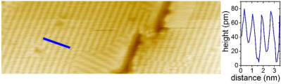
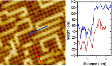
In Fig. 1 we present such a (21) reconstructed surface area. The height scan taken along the blue line as indicated in the topography is consistent with the aforementioned idea of each second row of Sm atoms missing. This is corroborated by a change in height on and between these rows of atoms of the order 40–50 pm; yet, an order of magnitude smaller height oscillations for the (21) reconstructed surface was also reported Yee et al. (2013); Pirie et al. (2020). The reconstruction is likely formed during the cleaving process or subsequently upon some additional diffusion of surface atoms. In both cases, one may expect domains of (21) and (12) reconstructed areas and dislocations between the Sm rows by one lattice constant, both of which can easily be recognized in the topography, Fig. 1.
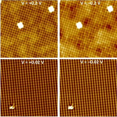
Rarely we also found atomically flat surface areas as shown in Fig. 2. Similar surface topographies have been presented before Ruan et al. (2014); Rößler et al. (2014); Sun et al. (2018); Herrmann et al. (2020); Yee et al. (2013); Jiao et al. (2016); Matt et al. (2018). It was shown, however, that the obtained topography depends on applied bias voltage , and even a contrast reversal was observed for 0.2 V and 3.0 V Herrmann et al. (2020). In the following we make use the dual-bias mode described in Section II as it allows to visualize exactly the same surface area without relying on defects on top of the investigated surface (the appearance of defects may change with , see Fig. 2). We have chosen values of small compared to the barrier height (see also below) yet larger than the hybridization gap of less than 20 meV Zhang et al. (2013); Xu et al. (2013); Frantzeskakis et al. (2013); Fuhrman et al. (2018); Valentine et al. (2018); Sun et al. (2018). In Fig. 2 dual-mode topographies for 0.2 V (upper) and 0.02 V (lower) are compared. Note that here different samples were investigated at somewhat different temperatures of 6 K (upper) and 1.7 K (lower). Qualitatively, the topographies for given temperature agree very well, i.e. there is no contrast inversion of reversed . There are subtle inhomogeneities in the background at 6 K; we can only speculate that they result from a not fully developed conducting surface state because we so far did not observe such inhomogeneities at 1.7 K (see also discussion of Fig. 7 below). We note that very similar inhomogeneities are reported on atomically flat surfaces, Fig. S1B in Pirie et al. (2020).
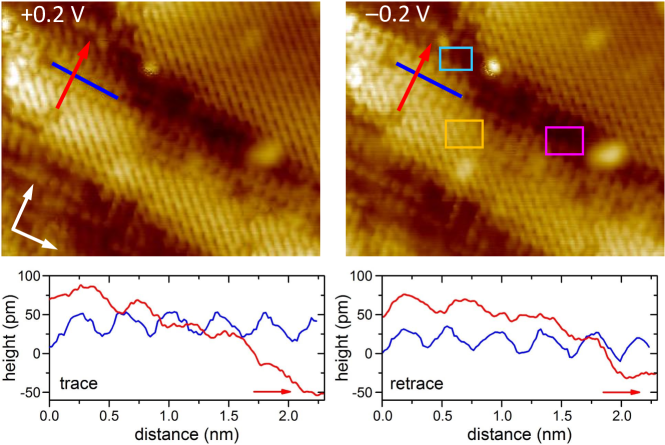
To investigate the surface termination in more detail we present in Fig. 3 topographies on areas exhibiting steps of less than one unit cell height Rößler et al. (2014). Such steps are perfectly suited to gain information about the different surface terminations. Again, the topographies obtained in dual mode with 0.2 V agree on a qualitative level. The white arrows in Fig. 3 indicate the main crystallographic directions and . Height scans taken along the blue lines, i.e. parallel to one of the main crystallographic directions and at overall unchanged height, clearly indicate lateral distances between corrugations consistent with the lattice constant , while such taken along descending height (red arrows) exhibit less obvious corrugations (possibly related to crystallographic imperfections within such regions of changing overall height). Within elevated areas (bright regions), however,
the corrugations appear to run along the diagonal, i.e. , directions. This is consistent Ruan et al. (2014); Rößler et al. (2014) with a Sm-terminated surface where also, in addition to the Sm atoms, the apex atoms of the B-octahedra are seen, see discussion of Fig. 8 below as well as the crystal structure shown in Fig. 4.
We now turn to the height scans taken along the red arrows in the topographies which, again, follow a direction but also include a height change. Atomic
distances corresponding to can be seen for 0.2 V, but less well for 0.2 V. Clearly, the total change in height depends to some extent on : It amounts to about 130 pm for 0.2 V and 100 pm for 0.2 V. Yet, both numbers appear to be consistent with the expected step height upon going from a Sm- to a B-terminated surface considering the inter-octahedron B distance of 164.6 pm. Given the fact that distances of are observed along the main crystallographic directions on this plane such a step height is difficult to interpret otherwise; a viable alternative is the opposite assignment (i.e. going from a B-terminated surface down to a Sm-terminated one) which would, however, involve breaking up of B-otcahedra, i.e. intra-octahedral bond breaking. Estimates of the surface energy Sun et al. (2018); Rößler et al. (2016) indicate a slight preference for inter-octahedral bond breaking but impurities or sample inhomogeneities and defects may change
these estimates locally. Indeed, a donut-like structure was interpreted as breaking inter-octahedral bonds Ruan et al. (2014).
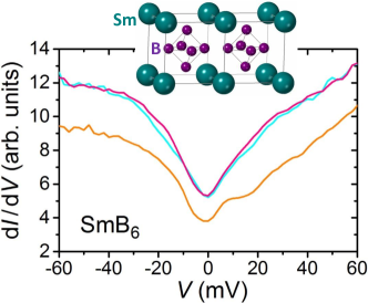
In order to gain further insight into the different terminations exposed in Fig. 3 tunneling spectroscopy was conducted. The STS curves shown in Fig. 4 correspond in color to the areas marked in Fig. 3 (right) over which the spectra were averaged. These spectra can be compared to those obtained on small areas of atomically flat surfaces, but differ from those seen on larger areas in that there is no pronounced maximum in d/d at around mV Rößler et al. (2014). The orange spectrum attained on the elevated part of the topography Fig. 3 exhibits a well developed hump at mV Ruan et al. (2014); Rößler et al. (2014); Miyamachi et al. (2017). It is tempting to compare this hump to the conspicuous maximum observed on Sm-terminated surface of larger areas Ruan et al. (2014); Rößler et al. (2014). Note that we did not observe (Fig. 4 and Rößler et al. (2014)) a pronounced shift in energy of features at negative as reported elsewhere Matt et al. (2018).
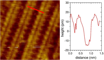
The discussion above indicated that a reconstruction is energetically favorable with respect to the polar nature of a Sm- or B-terminated surface. However, a similar effect is conceivable if the reconstruction is not long-ranged, but realized only locally. The lines of Sm may then meander Rößler et al. (2014, 2016) not giving rise to a
superstructure Frantzeskakis et al. (2013). Part of such a “disordered” reconstructed surface is shown in Fig. 5. In such a case, a similar change in height upon going from the topmost Sm atoms to the underlying B layer is expected as in Fig. 3. The height scan, Fig. 5 (right), along the red line marked in the topography indeed supports this assertion.
In one instance, we observed a topography as presented in Fig. 6. The height scan may be interpreted as every third row of atoms missing. Here, the height change between the upper and lower rows of atoms is only about 30 pm, similar to Rößler et al. (2014) or slightly smaller (Fig. 1) than the case of reconstructions. The exact number, however, may depend on details of the tip, i.e. how well it may penetrate between the rows of atoms, and may even be much smaller Pirie et al. (2020); Yee et al. (2013).
It should be noted again that our assignment of Sm- or B-terminated surfaces depends largely on the exact cleave, i.e. whether inter- or intra-octahedral bonds are broken. Albeit the former is, as mentioned above, energetically favorable, the latter may also occur as suggested by the observation of so-called donuts Ruan et al. (2014); Rößler et al. (2016).
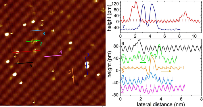
In Fig. 7 we present a topography over an area of 40 nm40 nm. While we have certainly encountered areas showing a smaller number of defects Jiao et al. (2016) it provides an overview of the different types of defects found on a B-terminated surface. The largest protrusions, #1 (red) and #7 (dark blue) in the upper right panel, with heights well beyond 100 pm are most likely caused by adatoms on top of the surface. The short red dashes in the height scan mark distances of suggesting that the underlying lattice is not disturbed beyond the defects. Other defects, #5 (orange) and #6 (black) in the lower right panel, appear to be incorporated into the lattice as also the immediate lattice sites seem influenced. Albeit conceivable, there is no evidence for an exchange of B by Al in pure SmB6 Konovalova et al. (1982) (note that this refers to substitution of individual B atoms by Al, not to Al inclusion of non-negligible size Phelan et al. (2016); Thomas et al. (2019)). In the Th-Pd-B system it was found that Pd may replace two adjacent B atoms belonging to neighbouring octahedra Zandbergen et al. (1994). Along the same line one may speculate that a similar replacement of adjacent B atoms by impurities near the surface may result in the observed slight displacement of surface atoms. Qualitatively different are the defects #3 (light blue) and #4 (magenta). Here, the lateral position (again, the vertical dashes indicate distances of ) and the height oscillation of the protrusions appear to remain unchanged while the height level is either raised (#3) or lowered (#4) by about 15–20 pm over distances of about 2 lattice constants from the center of the defect. We speculate that the defect itself is located in a subsurface layer, possibly on a Sm site, leaving the B-octahedra intact. It should be noted that this type of defect seems qualitatively different from the background inhomogeneity of Fig. 2. Albeit a clear assignment of either one of these features to structural or electronic inhomogeneities is speculative at present, it is obvious that a clean surface is a prerequisite for their observation. It should also be noted that dents of about 80 pm have so far only been observed on Sm-terminated surfaces Rößler et al. (2014). The topography of such dents is very similar to the surface structure of La-terminated LaB6 where La atoms are missing from the topmost layer Ozcomert and Trenary (1992). Therefore, it should be highly instructive to investigate Sm-deficient samples Sm1-xB6 and attempt to correlate the Sm-deficiency with the occurrence of these dents.
III.2 EuB6
In contrast to SmB6, the ferromagnetic semimetal EuB6 has so far only scarcely been investigated by STM Pohlit et al. (2018) even though its electronic structure is not fully understood, see Zhang et al. (2008); Massidda et al. (1997) and references therein. Hence, STS—in particular by using a spin-polarized tip—may provide fresh insight. In the following, we focus on the surface topography.
In Fig. 8 we compare the topographies of rare-earth terminated samples EuB6 and SmB6. In both cases, atomically flat and clean surface areas could be found after cleaving. The blue lines in the topographies indicate where the height scans parallel to the crystallographic directions were taken. The corrugations of heights 30–40 pm are spaced apart by one respective lattice constant . However, at the center of the square arrangements of these main corrugations in the topography
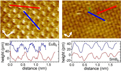
(resulting from the cubic structure) additional humps are seen, also forming a regular, square arrangement. This is evidenced by the red height scans along the diagonal directions, with the distances between the main and the interjacent smaller corrugations corresponding to . Based on the distances and orientations, the higher protrusions were assigned Ruan et al. (2014); Rößler et al. (2014) to the rare-earth atoms and the smaller ones to the apex of the B octahedra, again assuming breaking inter-octahedral bonds upon cleaving. We emphasize that the observation of interjacent smaller corrugations along is pivotal for the assignment of the surface termination, yet requires sufficiently large, atomically flat and clean surface areas. However, the consistent observation of this type of
surface topography on two different members of the hexaboride family makes a plausible case.
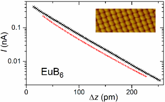
Based on DFT calculations it was suggested that the work function for a Sm-terminated surface of SmB6 is about 2 eV, and at least twice as high on a B-terminated surface Sun et al. (2018). We therefore started to investigate the tunneling barrier height , which is related to the work functions of
the sample and the tip ( and , respectively). The tunneling current decreases exponentially with increasing tip-sample distance , i.e. . The barrier height can be calculated from , where is the bare electron mass. Figure 9 shows two curves obtained on a clean B-terminated EuB6 surface shown in the inset. The barrier heights for the two exemplary curves are 4.7 eV and 5.6 eV, i.e. they vary by almost 1 eV. Unfortunately, because of their highly infrequent occurrence we were not able so far to measure on a Eu-terminated surface. It therefore remains to be seen whether a measurement of the barrier height can help in identifying the termination of clean EuB6 surfaces.
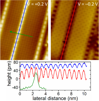
In the case of SmB6, both the investigation of slightly Gd-substituted samples with W tunneling tips and of pristine SmB6 with Cr tips resulted in a strong suppression of the surface state Jiao et al. (2018). In fact, the d/d curves in close proximity to magnetic defects and taken with magnetic tip are akin to spectra obtained with W tip on pristine SmB6 at 20 K, a temperature high enough such that the surface states do not significantly contribute to the tunneling spectra. These observations are expected for topologically nontrivial surface states close to atoms carrying a sizable magnetic moment arising from an exchange interaction Liu et al. (2009); Wang et al. (2010). Given this achievement in utilizing Cr tips as well as the magnetic properties of EuB6 we also started to investigate surfaces of EuB6 with magnetic Cr tunneling tips. One particularly intriguing example, attained in dual-bias mode for V, is presented in Fig. 10. The dual-bias mode is important as an only partial contrast reversal for the two different -values is observed, rendering a position adjustment of subsequently obtained images based solely on defects less reliable. This partial contrast reversal also complicates the assignment of the observed features: While the prominent bright lines seen for V correspond in height (see green scan line and green height profile) to Sm atoms, Fig. 5, and might be interpreted as Eu atoms, the same lines appear dark, i.e. as dents, for V. We note that by utilizing a magnetic tip, contrast changes may be expected mostly on surfaces of magnetic materials. Importantly, the height profiles measured along these lines did not show any contrast reversal upon reversing (compare the blue and red height scans in Fig. 10). The corrugations along these lines exhibit a periodicity of . Taken together, one may speculate about the formation of magnetic Eu dimers on the surface of EuB6. Clear of these lines, there is no obvious indication for a formation of such dimers: The green height scan exhibits corrugations (away from the aforementioned line) with distances corresponding to . However, the apparent changes in contrast in areas between the line features upon reversal of render this picture incomplete, at least. Clearly, measurements in magnetic fields are called for, but so far we were not able to locate such a topographic feature in our STM system with magnetic field capabilities.
IV Conclusions
Investigating topographies on a large number of SmB6 and EuB6 samples revealed different surface terminations which show similarities between these two hexaborides. Such similarities are obvious for the rare-earth terminated surfaces, a termination that is rather rare Ruan et al. (2014); Rößler et al. (2014) but essential when attempting an assignment of the different terminations. In addition, utilizing a dual-bias mode allowed a comparison of topographies obtained with different bias voltages on exactly identical surface areas without relying on defects. Along with the observations of step heights less than , these observations made a reliable assignment of the rare-earth and B-terminated surfaces possible. Apart from these atomically flat terminations, we observed different line structures which may correspond to lines of rare-earth atoms on top of an otherwise B-terminated surfaces. Some of these structures exhibited intriguing properties, also if probed by magnetic tips, which warrants further study.
V Acknowledgement
We thank Silvia Seiro, Ulrich K. Rößler, Frank Steglich, Hao Tjeng and Jens Wiebe for support and discussions. Financial support from the Deutsche Forschungsgemeinschaft within the priority program SPP1666 is gratefully acknowledged. Work at Los Alamos was performed under the auspices of the U.S. Department of Energy, Office of Basic Energy Sciences, Division of Materials Science and Engineering.
References
- Etourneau and Hagenmuller (1985) J. Etourneau and P. Hagenmuller, Philos. Mag. 52, 589 (1985).
- Berrada et al. (1978) A. Berrada, J. P. Mercurio, J. Etourneau, and P. Hagenmuller, J. Less-Common Met. 59, 7 (1978).
- Young et al. (1999) D. P. Young, D. Hall, M. E. Torelli, Z. Fisk, J. L. Sarrao, J. D. Thompson, H. R. Ott, S. B. Oseroff, R. G. Goodrich, and R. Zysler, Nature 397, 412 (1999).
- Stankiewicz et al. (2014) J. Stankiewicz, J. Sesé, G. Balakrishnan, and Z. Fisk, Phys. Rev. B 90, 155128 (2014).
- Effantin et al. (1985) J. M. Effantin, J. Rossatmignod, P. Burlet, H. Bartholin, S. Kunii, and T. Kasuya, J. Magn. Magn. Mater. 47-48, 145 (1985).
- Grushko et al. (1985) Y. S. Grushko, Y. B. Paderno, K. Y. Mishin, L. I. Molkanov, G. A. Shadrina, E. S. Konovalova, and E. M. Dudnik, Phys. Stat. Sol. B 128, 591 (1985).
- Vainshtein et al. (1965) E. E. Vainshtein, S. M. Blokhin, and Y. B. Paderno, Sov. Phys.-Solid State 6, 2318 (1965).
- Utsumi et al. (2017) Y. Utsumi, D. Kasinathan, K.-T. Ko, S. Agrestini, M. W. Haverkort, S. Wirth, Y.-H. Wu, K.-D. Tsuei, D.-J. Kim, Z. Fisk, A. Tanaka, P. Thalmeier, and L. H. Tjeng, Phys. Rev. B 96, 155130 (2017).
- Dzero et al. (2010) M. Dzero, K. Sun, V. Galitski, and P. Coleman, Phys. Rev. Lett. 104, 106408 (2010).
- Aeppli and Fisk (1992) G. Aeppli and Z. Fisk, Comments Cond. Mat. Phys. 16, 155 (1992).
- Riseborough (2000) P. S. Riseborough, Adv. Phys. 49, 257 (2000).
- Takimoto (2011) T. Takimoto, J. Phys. Soc. Jpn. 80, 123710 (2011).
- Lu et al. (2013) F. Lu, J. Zhao, H. Weng, Z. Fang, and X. Dai, Phys. Rev. Lett. 110, 096401 (2013).
- Kim et al. (2014a) J. Kim, K. Kim, C.-J. Kang, S. Kim, H. C. Choi, J.-S. Kang, J. D. Denlinger, and B. I. Min, Phys. Rev. B 90, 075131 (2014a).
- Xu et al. (2014) N. Xu, P. K. Biswas, J. H. Dil, R. S. Dhaka, G. Landolt, S. Muff, C. E. Matt, X. Shi, N. C. Plumb, M. Radović, E. Pomjakushina, K. Conder, A. Amato, S. V. Borisenko, R. Yu, H. M. Weng, Z. Fang, X. Dai, J. Mesot, H. Ding, and M. Shi, Nature Commun. 5, 4566 (2014).
- Suga et al. (2014) S. Suga, K. Sakamoto, T. Okuda, K. Miyamoto, K. Kuroda, A. Sekiyama, J. Yamaguchi, H. Fujiwara, A. Irizawa, T. Ito, S. Kimura, T. Balashov, W. Wulfhekel, S. Yeo, F. Iga, and S. Imada, J. Phys. Soc. Jpn. 83, 014705 (2014).
- Wolgast et al. (2013) S. Wolgast, C. Kurdak, K. Sun, J. W. Allen, D.-J. Kim, and Z. Fisk, Phys. Rev. B 88, 180405(R) (2013).
- Eo et al. (2019) Y. S. Eo, A. Rakoski, J. Lucien, D. Mihaliov, C. Kurdak, P. F. S. Rosa, and Z. Fisk, Proc. Natl. Acad. Sci. USA 116, 12638 (2019).
- Hlawenka et al. (2018) P. Hlawenka, K. Siemensmeyer, E. Weschke, A. Varykhalov, J. Sánchez-Barriga, N. Y. Shitsevalova, A. V. Dukhnenko, V. B. Filipov, S. Gabáni, K. Flachbart, O. Rader, and E. D. L. Rienks, Nature Commun. 9, 517 (2018).
- Baruselli and Vojta (2015) P. P. Baruselli and M. Vojta, Phys. Rev. Lett. 115, 156404 (2015).
- Legner et al. (2015) M. Legner, A. Rüegg, and M. Sigrist, Phys. Rev. Lett. 115, 156405 (2015).
- Sundermann et al. (2018) M. Sundermann, H. Yavas, K. Chen, D. Kim, Z. Fisk, D. Kasinathan, M. Haverkort, P. Thalmeier, A. Severing, and L. Tjeng, Phys. Rev. Lett. 120, 016402 (2018).
- Antonov et al. (2002) V. N. Antonov, B. N. Harmon, and A. N. Yaresko, Phys. Rev. B 66, 165209 (2002).
- Kang et al. (2015) C.-J. Kang, J. Kim, K. Kim, J. Kang, J. D. Denlinger, and B. I. Min, J. Phys. Soc. Jpn. 84, 024722 (2015).
- Min et al. (2017) C.-H. Min, F. Goth, P. Lutz, H. Bentmann, B. Y. Kang, B. K. Cho, J. Werner, K.-S. Chen, F. Assaad, and F. Reinert, Sci. Rep. 7, 11980 (2017).
- Zhu et al. (2013) Z.-H. Zhu, A. Nicolaou, G. Levy, N. P. Butch, P. Syers, X. F. Wang, J. Paglione, G. A. Sawatzky, I. S. Elfimov, and A. Damascelli, Phys. Rev. Lett. 111, 216402 (2013).
- Ruan et al. (2014) W. Ruan, C. Ye, M. Guo, F. Chen, X. Chen, G.-M. Zhang, and Y. Wang, Phys. Rev. Lett. 112, 136401 (2014).
- Rößler et al. (2014) S. Rößler, T.-H. Jang, D. J. Kim, L. H. Tjeng, Z. Fisk, F. Steglich, and S. Wirth, Proc. Natl. Acad. Sci. USA 111, 4798 (2014).
- Sun et al. (2018) Z. Sun, A. Maldonado, W. S. Paz, D. S. Inosov, A. P. Schnyder, J. J. Palacios, N. Y. Shitsevalova, V. B. Filipov, and P. Wahl, Phys. Rev. B 97, 235107 (2018).
- Pirie et al. (2020) H. Pirie, Y. Liu, A. Soumyanarayanan, P. Chen, Y. He, M. M. Yee, P. F. S. Rosa, J. D. Thompson, D.-J. Kim, Z. Fisk, X. Wang, J. Paglione, D. K. Morr, M. H. Hamidian, and J. E. Hoffman, Nature Phys. 16, 52 (2020).
- Rößler et al. (2016) S. Rößler, L. Jiao, D. J. Kim, S. Seiro, K. Rasim, F. Steglich, L. H. Tjeng, Z. Fisk, and S. Wirth, Philos. Mag. 96, 3262 (2016).
- Herrmann et al. (2020) H. Herrmann, P. Hlawenka, K. Siemensmeyer, E. Weschke, J. Sánchez-Barriga, A. Varykhalov, N. Y. Shitsevalova, A. V. Dukhnenko, V. B. Filipov, S. Gabáni, K. Flachbart, O. Rader, M. Sterrer, and E. D. L. Rienks, Adv. Mater. 32 (2020), doi:10.1002/adma.201906725.
- Zhang et al. (2008) X. Zhang, S. von Molnár, Z. Fisk, and P. Xiong, Phys. Rev. Lett. 100, 167001 (2008).
- Süllow et al. (1998) S. Süllow, I. Prasad, M. C. Aronson, J. L. Sarrao, Z. Fisk, D. Hristova, A. H. Lacerda, M. F. Hundley, A. Vigliante, and D. Gibbs, Phys. Rev. B 57, 5860 (1998).
- Pohlit et al. (2018) M. Pohlit, S. Rößler, Y. Ohno, H. Ohno, S. von Molnár, Z. Fisk, J. Müller, and S. Wirth, Phys. Rev. Lett. 120, 257201 (2018).
- Ramankutty et al. (2016) S. V. Ramankutty, N. de Jong, Y. K. Huang, B. Zwartsenberg, F. Massee, T. V. Bay, M. S. Golden, and E. Frantzeskakis, J. Electron Spectrosc. Relat. Phenom. 208, 43 (2016).
- Fisk et al. (1979) Z. Fisk, D. Johnston, B. Cornut, S. von Molnár, S. Oseroff, and R. Calvo, J. Appl. Phys. 50, 1911 (1979).
- Kim et al. (2014b) D. J. Kim, J. Xia, and Z. Fisk, Nature Mater. 13, 466 (2014b).
- Rosa and Fisk (2018) P. F. S. Rosa and Z. Fisk, in Crystal Growth of Intermetallics, edited by P. Gille and Y. Grin (Berlin, Boston: De Gruyter, 2018) pp. 49–60.
- (40) Omicron Nanotechnology GmbH, Taunusstein (Germany).
- Schubert et al. (2012) G. Schubert, H. Fehske, L. Fritz, and M. Vojta, Phys. Rev. B 85, 201105(R) (2012).
- Wolgast et al. (2015) S. Wolgast, Y. S. Eo, T. Öztürk, G. Li, Z. Xiang, C. Tinsman, T. Asaba, B. Lawson, F. Yu, J. W. Allen, K. Sun, L. Li, C. Kurdak, D.-J. Kim, and Z. Fisk, Phys. Rev. B 92, 115110 (2015).
- Yee et al. (2013) M. M. Yee, Y. He, A. Soumyanarayanan, D.-J. Kim, Z. Fisk, and J. E. Hoffman, “Imaging the Kondo insulating gap on SmB6.” (2013), arXiv:1308.1085.
- Miyazaki et al. (2012) H. Miyazaki, T. Hajiri, T. Ito, S. Kunii, and S. I. Kimura, Phys. Rev. B 86, 075105 (2012).
- Miyamachi et al. (2017) T. Miyamachi, S. Suga, M. Ellguth, C. Tusche, C. M. Schneider, F. Iga, and F. Komori, Sci. Rep. 7, 12837 (2017).
- Buchsteiner et al. (2019) P. Buchsteiner, F. Sohn, J. G. Horstmann, J. Voigt, M. C. Hatnean, G. Balakrishnan, C. Ropers, P. E. Blöchl, and M. Wenderoth, Phys. Rev. B 100, 205407 (2019).
- Yoo and Weitering (2002) K. Yoo and H. H. Weitering, Phys. Rev. B 65, 115424 (2002).
- Jiao et al. (2016) L. Jiao, S. Rößler, D. J. Kim, L. H. Tjeng, Z. Fisk, F. Steglich, and S. Wirth, Nature Commun. 7, 13762 (2016).
- Matt et al. (2018) C. E. Matt, H. Pirie, A. Soumyanarayanan, M. M. Yee, Y. He, D. T. Larson, W. S. Paz, J. J. Palacios, M. H. Hamidian, and J. E. Hoffman, “Consistency between ARPES and STM measurements on SmB6.” (2018), arXiv:1810.13442.
- Zhang et al. (2013) X. Zhang, N. P. Butch, P. Syers, S. Ziemak, R. L. Greene, and J. Paglione, Phys. Rev. X 3, 011011 (2013).
- Xu et al. (2013) N. Xu, X. Shi, P. K. Biswas, C. E. Matt, R. S. Dhaka, Y. Huang, N. C. Plumb, M. Radović, J. H. Dil, E. Pomjakushina, K. Conder, A. Amato, Z. Salman, D. M. Paul, J. Mesot, H. Ding, and M. Shi, Phys. Rev. B 88, 121102 (2013).
- Frantzeskakis et al. (2013) E. Frantzeskakis, N. de Jong, B. Zwartsenberg, Y. K. Huang, Y. Pan, X. Zhang, J. X. Zhang, F. X. Zhang, L. H. Bao, O. Tegus, A. Varykhalov, A. de Visser, and M. S. Golden, Phys. Rev. X 3, 041024 (2013).
- Fuhrman et al. (2018) W. T. Fuhrman, J. R. Chamorro, P. Alekseev, J.-M. Mignot, T. Keller, J. A. Rodriguez-Rivera, Y. Qiu, P. Nikolić, T. M. McQueen, and C. L. Broholm, Nature Commun. 9, 1539 (2018).
- Valentine et al. (2018) M. E. Valentine, S. Koohpayeh, W. A. Phelan, T. M. McQueen, P. F. S. Rosa, Z. Fisk, and N. Drichko, Physica B 536, 60 (2018).
- Konovalova et al. (1982) E. S. Konovalova, Y. B. Paderno, T. Lundstrem, L. D. Finkel’shtein, N. N. Efremova, and E. M. Dudnik, Powder Metall Met. Ceram. 21, 820 (1982).
- Phelan et al. (2016) W. A. Phelan, S. M. Koohpayeh, P. Cottingham, J. A. Tutmaher, J. C. Leiner, M. D. Lumsden, C. M. Lavelle, X. P. Wang, C. Hoffmann, M. A. Siegler, N. Haldolaarachchige, D. P. Young, and T. M. McQueen, Sci. Rep. 6, 20860 (2016).
- Thomas et al. (2019) S. Thomas, X. Ding, F. Ronning, V. Zapf, J. Thompson, Z. Fisk, J. Xia, and P. Rosa, Phys. Rev. Lett. 122, 166401 (2019).
- Zandbergen et al. (1994) H. W. Zandbergen, T. J. Gortenmulder, J. L. Sarrac, J. C. Harrison, M. C. de Andrade, J. Hermann, S. H. Han, Z. Fisk, M. B. Maple, and R. J. Cava, Physica C 232, 328 (1994).
- Ozcomert and Trenary (1992) J. S. Ozcomert and M. Trenary, Surf. Sci. Lett. 265, L227 (1992).
- Massidda et al. (1997) S. Massidda, A. Continenza, T. M. de Pascale, and R. Monnier, Z. Phys. B: Condens. Matter 102, 83 (1997).
- Jiao et al. (2018) L. Jiao, S. Rößler, D. Kasinathan, P. F. S. Rosa, C. Guo, H. Yuan, C.-X. Liu, Z. Fisk, F. Steglich, and S. Wirth, Sci. Adv. 4, eaau4886 (2018).
- Liu et al. (2009) Q. Liu, C.-X. Liu, C. Xu, X.-L. Qi, and S.-C. Zhang, Phys. Rev. Lett. 102, 156603 (2009).
- Wang et al. (2010) Q.-H. Wang, D. Wang, and F.-C. Zhang, Phys. Rev. B 81, 035104 (2010).