Realistic flat-band model based on degenerate -orbitals
in two-dimensional ionic materials
Abstract
Though several theoretical models have been proposed to design electronic flat-bands, the definite experimental realization in two-dimensional atomic crystal is still lacking. Here we propose a novel and realistic flat-band model based on threefold degenerate -orbitals in two-dimensional ionic materials. Our theoretical analysis and first-principles calculations show that the proposed flat-band can be realized in 1T layered materials of alkali-metal chalogenides and metal-carbon group compounds. Some of the former are theoretically predicted to be stable as layered materials (e.g., K2S), and some of the latter have been experimentally fabricated in previous works (e.g., Gd2CCl2). More interestingly, the flat-band is partially filled in the heterostructure of a K2S monolayer and graphene layers. The spin polarized nearly flat-band can be realized in the ferromagnetic state of a Gd2CCl2 monolayer, which has been fabricated in experiments. Our theoretical model together with the material predictions provide a realistic platform for the study of flat-bands and related exotic quantum phases.
Keywords: Flat-band, Degenerate orbitals, Material realization, 1T structure, Partially filled
1. Introduction
The properties including the electronic bands of a material are codetermined by its structure and the component elements of which the outer-shell electrons usually matter most harrison2012electronic . In the band theory regime, there are two limiting cases: the massless Dirac fermion in linear dispersion band neto2009electronic and infinitely heavy fermion in flat-band mielke1991ferromagnetism ; tasaki1992ferromagnetism . Both of them harbor unique and fantastic properties. The Dirac fermion has been experimentally realized in a graphene monolayer neto2009electronic . For the flat-band, the density of states is impressive and effects of interactions are entirely nonperturbative mielke1991ferromagnetism ; mielke1992exact ; tasaki1992ferromagnetism ; tasaki1998nagaoka ; bodyfelt2014flatbands . This may offer unique opportunities for the emergence of exotic quantum phases, including ferromagnetism mielke1992exact ; mielke1991ferromagnetism ; tasaki1992ferromagnetism ; tasaki1998nagaoka , high-temperature fractional quantum Hall effect tang2011high ; sun2011nearly ; neupert2011fractional , Bose-Einstein condensation huber2010bose , and high-temperature superconductivity imada2000superconductivity ; peotta2015superfluidity , Wigner crystalization wu2007flat .
The realization of flat-band and intriguing properties in various moiré superlattices has achieved great success cao2018unconventional ; cao2018correlated ; chen2019evidence ; ma2020topological , where the tunability due to the two-dimensional (2D) nature plays an important role. Compared with the flat-band in a small moiré Brillouin zone, the intrinsic flat-band in a whole Brillouin zone of 2D atomic crystal is also attractive and may have its own merit for realization of above exotic quantum phases. To design flat-band in the 2D crystals, several theoretical models have been proposed, including single (e.g., - or -type) orbital in systems of bipartite graphs or their line graphs mielke1992exact ; mielke1991ferromagnetism ; tasaki1992ferromagnetism ; tasaki1998nagaoka ; bodyfelt2014flatbands ; tang2011high ; sun2011nearly ; neupert2011fractional ; huber2010bose ; imada2000superconductivity ; peotta2015superfluidity ; lieb1989two ; wang2011nearly ; leykam2018artificial ; chernyshev2016damped ; guo2009topological ; weeks2010topological ; bergman2008band ; yang2020gapped , and twofold degenerate -type orbital in honeycomb structure wu2007flat . Though progress has been made slot2017experimental ; hase2018possibility ; aiura2017disappearance ; lin2018flatbands ; leykam2018artificial ; drost2017topological ; kang2020dirac ; yin2019negative ; PhysRevLettFlat , the definitive experimental realization in 2D atomic crystal is still lacking. In real 2D materials, the electronic structures often deviate heavily or even completely from these idealized models, when there is inevitable hybridization between the specified orbitals and other orbitals. From a more realistic consideration, the threefold degenerate -orbitals exist widely and isolate well from other orbitals in ionic materials. Designing a 2D flat-band based on the degenerate -orbitals and searching for its material realization may open a promising way.
In this paper, we propose a novel and realistic flat-band model based on the degenerate -orbitals when they locate at the centers of octahedrons which are closely-packed to form a 2D structure. Our theoretical analysis and first-principles calculations show that the proposed flat-bands can be realized in 1T layered materials of alkali-metal chalogenides and metal-carbon group compounds. The calculated flat-bands of these materials can be well-described by our theoretical model with physically meaningful parameters. Some of the former materials are theoretically predicted to be stable in layered structure here (e.g., K2S), while some of the latter have been experimentally fabricated in previous works (e.g., Gd2CCl2) schleid1994crystal ; ryazanov2006la2tei2 ; schleid1987synthesis ; lukachuk2007new . More interestingly, the flat-band is partially filled in the heterostructure of K2S and graphene layers. The spin polarized nearly flat-band can be realized in the ferromagnetic state of a Gd2CCl2 monolayer. Our theoretical model together with the material predictions provide a realistic platform for the study of flat-band and related exotic quantum phases.
2. Theoretical model
We first discuss the tight-binding (TB) model. In a 1T (tetragonal symmetry, octahedral coordination) layered structure, the octahedrons are closely-packed in 2D planes by sharing edges and corners, as shown in Fig. 1. We define the 2D plane formed by the centers of octahedrons as -plane. Three lattice vectors in the -plane are defined as , , and , where is the lattice constant and are the unit vectors of the two orthogonal axes. When an anion locates at the center of an octahedron structure, its three -orbitals are energetically degenerate, as shown in Fig. 1a. For convenience, we label as and align their polarization direction to the three diagonals of the regular octahedron. Cations locate at the corners of octahedrons to make the system electronically neutral. The TB Hamiltonian reads
| (1) | ||||
| (2) |
where ; runs the locations of all anions in the -plane; describes the hopping between -orbitals on neighboring anions when their polarization directions cross at one corner of the octahedron, namely a cation; () describes the neighboring hopping between the same -orbitals when they are (not) perpendicular to the connection direction ; is the hopping between different -orbitals when only one of them is perpendicular to the connection direction . The values can be estimated as , where are the atomic potentials of the nearest cations. The schematic diagrams of hoppings along direction are shown in Fig. 1c. The gray solid circles represent the that are most contributive. It is obvious that is the only one case that wave functions and , and atomic potentials overlap directly. Thus, the amplitude of is expected to be apparently larger than , , and . describes the crystal field when the octahedrons are arranged in the 2D plane and the effect of structure adjustment, which is tunable via adjusting the structure or varying the chemical environment.
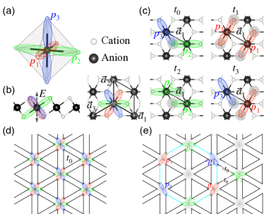
It is of practically guiding significance to consider a limiting case when only has nonzero value with and . Fig. 1d shows a schematic diagram of the lattice structure of . In momentum space, we define the three component basis as
| (3) |
Then takes the matrix form as
| (4) |
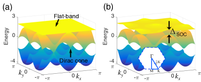
where is defined in the 2D Brillouin zone. The band structure contains three bands and , as shown in Fig. 2a. Interestingly, the band is totally flat over the entire 2D Brillouin zone . On the other hand, the bands are dispersive exhibiting eight Dirac cones at K and K points in the first Brillouin zone . The bandwidth of is determined by the amplitude of . The dispersive band and flat-band are energetically degenerate at and M points. The totally flat-band is attributed to the frustrated hopping nature bergman2008band . The loop in Fig. 1e represents a compact localized state and the frustrated hopping to a neighbor orbital.
With regard to spin-orbit coupling (SOC), we consider the original atomic form: liu2011low ; liu2013flat . It reads
| (5) |
where are Pauli matrices liu2011low ; liu2013flat . As shown in Fig. 2b, the band degeneracy lifts at the high symmetry , M, and K points due to the effects from SOC. A global gap occurs, which isolates the flat-bands from other bands. The flat-band becomes slightly dispersive after taking finite and into consideration.
3. Material realization
With the help of first-principles calculations, we predict that two classes of layered materials may harbor nearly flat-bands: 1T layered alkali-metal chalogenides and metal-carbon group compounds. To be specific, we give 1T dipotassium monosulfide (K2S) monolayer and digadolinium monocarbide dichloride (Gd2CCl2) monolayer as two examples.
| Energy difference (eV/unit cell) | O | S | Se | Te | |
| K | 0.01 | 0.18 | 0.22 | 0.27 | |
| 0.51 | 0.45 | 0.42 | 0.37 | ||
| Rb | 0.09 | 0.30 | 0.34 | 0.42 | |
| 0.43 | 0.39 | 0.37 | 0.33 | ||
Our density functional theory (DFT) calculations are carried out using the Vienna ab initio simulation package (VASP) VASP1996 , where the projector augmented plane wave (PAW) method blochl1994projector ; kresse1999ultrasoft is adopted, and the generalized gradient approximation (GGA) in the framework of Perdew-Burke-Ernzerhof (PBE) perdew1996generalized is chosen for the exchange-correlation interaction. The magnetic and electronic properties of the Gd2CCl2 system are calculated based on the range-separated Heyd-Scuseria-Ernzerhof 2006 (HSE06) hybrid functional heyd2003hybrid ; krukau2006influence . A specific semi-empirical scheme (DFT-D2) grimme2006semiempirical is used to treat the van der Waals (vdW) type interaction. Phonon spectrum are obtained using the PHONOPY code Phonopy2015 .
Table I lists the comparisons of total energies of alkali-metal chalogenides in different structures. All the 1T monolayers are energetically more favored than their 2H (hexagonal symmetry, trigonal prismatic coordination) counterparts, which benefits the synthesis of high quality 2D samples. The 2D monolayer would be epitaxially grown and further stabilized on proper substrates hong2017atomic ; zhu2017multivalency ; ding2020exploring ; ding2019signature ; zeng2017half . The structural stabilities of these 1T materials are also checked by their nonnegative phonon spectra.
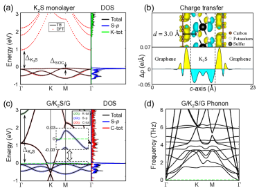
Some of the above 1T monolayered alkali-metal chalogenides harbor nearly flat-bands. As an example, the electronic band structures of the 1T K2S monolayer are shown in Fig. 3a. Our TB model fits well with the DFT calculated electronic bands with the parameters shown in the caption. The highest valence band is nearly flat with bandwidth of 55 meV. The atomic structure refers to Fig. 1. The optimized lattice constant is: .
Due to the 2D nature, monolayered materials can be conveniently stacked to form heterostructures. The charge transfer naturally takes place between the 2D materials when their work functions are different. Here, to explicitly show the doping effects on the flat-band materials, we theoretically study a G/K2S/G heterostructure in which a K2S layer is sandwiched in between two graphene layers. The lattice mismatch between a K2S unit cell and 22 graphene supercell is less than 2%. In Fig. 3b, the charge distribution is defined as , where , , and are the charge densities of the G/K2S/G heterostructure, K2S monolayer, and graphene layers, respectively. The calculated electrons transfer from the K2S layer to graphene layers is 0.13 electrons per unit cell. This evident value is mainly attributed to the large difference 3.0 eV in their work functions. Fig. 3c shows the orbital projected electronic bands. The nearly flat-band is partially filled and the Dirac points of graphene is shifted down below Fermi level due to the charge transfer effect. The filling level can be further tuned via electric gating due to the 2D nature. On the other hand, the nearly flat-band is almost intact from hybridization with other bands. The nonnegative phonon spectra in Fig. 3d verifies the structural stability. In addition, it notes that the band gap of a K2S monolayer is environmentally sensitive largely due to its ionic nature, as comparatively shown in Fig. 3a and c.
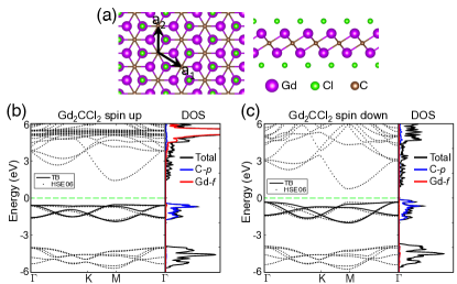
As another large family of materials, compounds of metal and carbon group elements can also adopt a 1T layered structure, some of which have been fabricated in experiments schleid1994crystal ; ryazanov2006la2tei2 ; schleid1987synthesis . We present a 1T Gd2CCl2 monolayer as a typical example. Fig. 4a shows the structure of a 1T Gd2CCl2 monolayer. In the 1T phase, one C atom sites at the inversion symmetry point of an octahedron formed by six Gd atoms. Different magnetic orders in a supercell are compared to find the ground state. Based on our HSE06 calculations, the Gd atoms prefer a ferromagnetic order. The ferromagnetic order could be further stabilized via applying external magnetic field deng2020quantum . Fig. 4b and c show the spin polarized band structures. Similar to the case of K2S monolayer, the highest valence band of the spin up electron in Gd2CCl2 is very flat with a bandwidth of 195 meV. From the orbital projected orbital projected density of states (DOS), it is clear that the three highest valence bands are mainly contributed from the -orbitals of C anions.
4. Discussion and conclusion
In summary, a novel TB model with (nearly) flat-bands was proposed based on the threefold degenerate -orbitals in 2D materials. As concrete examples, our calculations showed that a Gd2CCl2 monolayer harbors a spin polarized nearly flat-band in its ferromagnetic phase, and the flat-band is partially filled in the G/K2S/G heterostructure. Our theoretical model together with the material predictions provide a realistic platform for the study of flat-band and related exotic quantum phases.
Conflict of interest
The authors declare that they have no conflict of interest.
Acknowledgments
The authors thank Wei Qin and Zhenyu Zhang for helpful discussions. This work was supported by the National Basic Research Program of China (2015CB921102 and 2019YFA0308403), the National Natural Science Foundation of China (11674028 and 11822407), the Strategic Priority Research Program of Chinese Academy of Sciences (Grant No. XDB28000000), and China Postdoctoral Science Foundation (2020M670011).
Author contributions
Jiang Zeng and X. C. Xie conceived the idea and supervised the project. Jiang Zeng did the theoretical analysis and first-principles calculations. Jiang Zeng, Ming Lu, Hua Jiang, Haiwen Liu, and X. C. Xie analyzed the data and wrote the manuscript. All authors contributed to scientific discussion of the manuscript.
References
- (1) Harrison WA. Electronic structure and the properties of solids: the physics of the chemical bond. 2012.
- (2) Castro Neto AH, Guinea F, Peres NMR. The electronic properties of graphene. Rev Mod Phys 2009;81:109–162.
- (3) Mielke A. Ferromagnetism in the Hubbard model on line graphs and further considerations. J Phy A: Math Gen 1991;24:3311-3321.
- (4) Tasaki H. Ferromagnetism in the Hubbard models with degenerate single-electron ground states. Phys Rev Lett 1992;69:1608-1611.
- (5) Mielke A. Exact ground states for the Hubbard model on the kagome lattice. J Phy A: Math Gen 1992;25:4335–4345.
- (6) Tasaki H. From Nagaoka’s ferromagnetism to flat-band ferromagnetism and beyond: an introduction to ferromagnetism in the Hubbard model. Prog Theor Phys 1998;99:489–548.
- (7) Bodyfelt JD, Leykam D, Danieli C, et al. Flatbands under correlated perturbations. Phys Rev Lett 2014;113:236403.
- (8) Tang E, Mei JW, Wen XG. High-temperature fractional quantum Hall states. Phys Rev Lett 2011;106:236802.
- (9) Sun K, Gu ZC, Katsura H, et al. Nearly flatbands with nontrivial topology. Phys Rev Lett 2011;106:236803.
- (10) Neupert T, Santos L, Chamon C, et al. Fractional quantum Htall states at zero magnetic field. Phys Rev Lett 2011;106:236804.
- (11) Huber SD, Altman E. Bose condensation in flat bands. Phys Rev B 2010;82:184502.
- (12) Imada M, Kohno M. Superconductivity from flat dispersion designed in doped Mott insulators. Phys Rev Lett 2000;84:143–146.
- (13) Peotta S, Törmä P. Superfluidity in topologically nontrivial flat bands. Nat Commun 2015;6:8944.
- (14) Wu CJ, Bergman D, Balents L, et al. Flat bands and Wigner crystallization in the honeycomb optical lattice. Phys Rev Lett 2007;99:070401.
- (15) Cao Y, Fatemi V, Fang S, et al. Unconventional superconductivity in magic-angle graphene superlattices. Nature 2018;556:43–50.
- (16) Cao Y, Fatemi V, Demir A, et al. Correlated insulator behaviour at half-filling in magic-angle graphene superlattices. Nature 2018;556:80–84.
- (17) Chen G, Jiang LL, Wu S, et al. Evidence of a gate-tunable mott insulator in a trilayer graphene moiré superlattice. Nat Phys 2019;15:237–241.
- (18) Ma Z, Li S, Zheng YW, et al. Topological flat bands in twisted trilayer graphene. Sci Bull 2021, 66: 18-22.
- (19) Lieb EH. Two theorems on the Hubbard model. Phys Rev Lett 1989;62:1201–1204.
- (20) Wang F, Ran Y. Nearly flat band with Chern number = 2 on the dice lattice. Phys Rev B 2011;84:241103(R).
- (21) Leykam D, Andreanov A, Flach S. Artificial flat band systems: from lattice models to experiments. Adv Phy X 2018;3:1473052.
- (22) Chernyshev AL, Maksimov PA. Damped topological magnons in the kagome-lattice ferromagnets. Phys Rev Lett 2016;117:187203.
- (23) Guo HM, Franz M. Topological insulator on the kagome lattice. Phys Rev B 2009;80:113102.
- (24) Weeks C, Franz M. Topological insulators on the Lieb and perovskite lattices. Phys Rev B 2010;82:085310.
- (25) Bergman DL, Wu CJ, Balents L. Band touching from real-space topology in frustrated hopping models. Phys Rev B 2008;78:125104.
- (26) Yang YT, Jia ZY, Wu YJ, et al. Gapped topological kink states and topological corner states in honeycomb lattice. Sci Bull 2020;65:531–537.
- (27) Slot MR, Gardenier TS, Jacobse PH, et al. Experimental realization and characterization of an electronic Lieb lattice. Nat Phys 2017;13:672–676.
- (28) Hase I, Yanagisawa T, Aiura Y. Possibility of flat-band ferromagnetism in hole-doped pyrochlore oxides Sn2Nb2O7 and Sn2Ta2O7. Phys Rev Lett 2018;120:196401.
- (29) Aiura Y, Ozawa K, Hase I. Disappearance of localized valence band maximum of ternary tin oxide with pyrochlore structure, Sn2Nb2O7. J Phys Chem C 2017;121:9480–9488.
- (30) Lin ZY, Choi JH, Zhang Q, et al. Flatbands and emergent ferromagnetic ordering in Fe3Sn2 kagome lattices. Phys Rev Lett 2018;121:096401.
- (31) Drost R, Ojanen T, Harju A, et al. Topological states in engineered atomic lattices. Nat Phys 2017;13:668–671.
- (32) Kang MG, Ye LD, Fang S, et al. Dirac fermions and flat bands in the ideal kagome metal FeSn. Nat Mater 2020;19:163–169.
- (33) Yin JX, Zhang STS, Chang GQ, et al. Negative flat band magnetism in a spin–orbit-coupled correlated kagome magnet. Nat Phys 2019;15:443–448.
- (34) Baidya S, Mallik AV, Bhattacharjee S, et al. Interplay of magnetism and topological superconductivity in bilayer kagome metals. Phys Rev Lett 2020;125:026401.
- (35) Schleid T, Meyer G. Crystal structure of digadolinium monocarbide dichloride (1t type), Gd2CCl2. Zeitschrift für Kristallographie 1994;209:371–371.
- (36) Ryazanov M, Simon A, Mattausch H. La2TeI2: A new layered telluride iodide with unusual electrical properties. Inorg Chem 2006;45:10728–10733.
- (37) Schleid T, Meyer G. Synthesis and crystal structures of hydrogen and carbon stabilized lutetium monochloride, LuClHx and Lu2Cl2C. Zeitschrift für anorganische und allgemeine Chemie 1987;552:90–96.
- (38) Lukachuk M, Kremer RK, Mattausch H, et al. New layered germanide halides Re2GeX2 (Re= Y, Gd; X= Br, I). Inorg Chem 2007;46:3231–3235.
- (39) Liu CC, Jiang H, Yao YG. Low-energy effective hamiltonian involving spin-orbit coupling in silicene and two-dimensional germanium and tin. Phys Rev B 2011;84:95430.
- (40) Liu Z, Wang ZF, Mei JW, et al. Flat Chern band in a two-dimensional organometallic framework. Phys Rev Lett 2013;110:106804.
- (41) Kresse G, Furthmüller J. Efficient iterative schemes for total-energy calculations using a plane-wave basis set, Phys. Rev. B 1996;54:11169–11186.
- (42) Blöchl PE. Projector augmented-wave method. Phys Rev B 1994;50:17953-17979.
- (43) Kresse G, Joubert D. From ultrasoft pseudopotentials to the projector augmented-wave method, Phys Rev B 1999;59:1758-1775.
- (44) Perdew JP, Burke K, Ernzerhof M. Generalized gradient approximation made simple. Phys Rev Lett 1997;78:1397.
- (45) Heyd J, Scuseria GE, Ernzerhof M. Hybrid functionals based on a screened coulomb potential. J Chem Phys 2003;118:8207–8215.
- (46) Krukau AV, Vydrov OA, Izmaylov AF, et al. Influence of the exchange screening parameter on the performance of screened hybrid functionals. J Chem Phys 2006;125:224106.
- (47) Grimme F. Semiempirical GGA-type density functional constructed with a long-range dispersion correction. J Comput Chem 2006;27:1787–1799.
- (48) Togo A, Tanaka I. First principles phonon calculations in materials science. Scr Mater 2015;108:1–5.
- (49) Hong HK, Jo J, Hwang D, et al. Atomic scale study on growth and heteroepitaxy of ZnO monolayer on graphene. Nano Lett 2017;17:120–127.
- (50) Zhu ZL, Cai XL, Yi SH, et al. Multivalency-driven formation of Te-based monolayer materials: a combined first-principles and experimental study. Phys Rev Lett 2017;119:106101.
- (51) Ding WJ, Zeng J, Qin W, et al. Exploring high transition temperature superconductivity in a freestanding or SrTiO3-supported CoSb monolayer. Phys Rev Lett 2020;124:027002.
- (52) Ding C, Gong GM, Liu YZ, et al. Signature of superconductivity in orthorhombic CoSb monolayer films on SrTiO3(001). ACS Nano 2019;13:10434–10439.
- (53) Zeng J, Cui P, Zhang ZY. Half layer by half layer growth of a blue phosphorene monolayer on a GaN(001) substrate. Phys Rev Lett 2017;118:046101.
- (54) DengYJ, Yu YJ, Shi MZ, et al. Quantum anomalous hall effect in intrinsic magnetic topological insulator MnBi2Te4. Science 2020;367:895–900.