Towards highly efficient thin-film solar cells with a graded-bandgap CZTSSe layer
Faiz Ahmad,1 Akhlesh Lakhtakia,1,2,∗ Tom H. Anderson3 and Peter B. Monk3
1NanoMM–Nanoengineered Metamaterials Group, Department of Engineering Science and Mechanics, Pennsylvania State University, University Park, PA 16802-6812, USA
2Sektion for Konstruktion og Produktudvikling, Institut for Mekanisk Teknologi, Danmarks Tekniske Universitet, DK-2800 Kongens Lyngby, Danmark
3Department of Mathematical Sciences, University of Delaware, Newark, DE 19716, USA
∗Corresponding author. E–mail: akhlesh@psu.edu
Abstract
A coupled optoelectronic model was implemented along with the differential evolution algorithm to assess the efficacy of grading the bandgap of the Cu2ZnSn(SξSe1-ξ)4 (CZTSSe) layer for enhancing the power conversion efficiency of thin-film CZTSSe solar cells. Both linearly and sinusoidally graded bandgaps were examined, with the molybdenum backreflector in the solar cell being either planar or periodically corrugated. Whereas an optimally graded bandgap can dramatically enhance the efficiency, the effect of periodically corrugating the backreflector is modest at best. An efficiency of % is predicted with sinusoidal grading of a -nm-thick CZTSSe layer, in comparison to % efficiency achieved experimentally with a -nm-thick homogeneous CZTSSe layer. High electron-hole-pair generation rates in the narrow-bandgap regions and a high open-circuit voltage due to a wider bandgap close to the front and rear faces of the CZTSSe layer are responsible for the high enhancement of efficiency.
Keywords: Bandgap grading, optoelectronic optimization, thin-film solar cell, earth-abundant materials, CZTSSe solar cell
1 Introduction
As the worldwide demand for eco-responsible sources of cheap energy continues to increase for the betterment of an ever-increasing fraction of the human population [1], the cost of traditional crystalline-silicon solar cells continues to drop [2], as predicted earlier this decade [3]. While this is a laudable development, small-scale photovoltaic generation of energy must become ubiquitous for human progress to become truly unconstrained by energy economics. Thin-film solar cells are necessary for that to happen.
Currently, thin-film solar cells containing absorber layers made of either CIGS or CdTe are commercially dominant, even over their amorphous-silicon counterparts [4]. However, there is a strong concern about the planetwide availability of indium (In) and tellurium (Te), both needed for CIGS and CdTe solar cells [5]. Furthermore, both In and cadmium (Cd) are toxic, leading to environmental concerns about their impact following disposal after use.
Thin-film solar cells must be made from materials that are abundant on our planet and that can extracted, processed, and discarded with low environmental cost. Cu2ZnSn(SξSe1-ξ)4 (commonly referred as CZTSSe) is a -type semiconductor than can be used in place of CIGS in a solar cell. CZTSSe comprises nontoxic and abundant materials [6]. But the record for the power conversion efficiency of CZTSSe solar cells is only 12.6 [7, 8], which is substantially lower than the % record efficiency of CIGS solar cells [9, 10].
A low open-circuit voltage is the key limitation to high efficiency for CZTSSe solar cells [11, 12, 13]. This is due to
- (i)
-
(ii)
the high electron-hole recombination rate inside the CZTSSe layer because of the short lifetime of minority carriers (electrons) [16]; and
-
(iii)
the higher electron-hole recombination rate at the CdS/CZTSSe interface [17], an ultrathin CdS layer being employed as an -type semiconductor in the solar cell.
The low lifetime of minority carriers shortens their diffusion length, thereby limiting the collection of minority carriers deep in the CZTSSe absorber layer [16, 18]. For example, the diffusion length of electrons is less than 1 m when the bandgap of CZTSSe is eV (for ), which means that a solar cell with a CZTSSe layer of thickness m [18] will have a high series resistance [11, 19] that will have a deleterious effect on . Reduction of is therefore desirable, all the more so because it will reduce material usage and enhance manufacturing throughput concomitantly. But, a smaller will reduce the absorption of incident photons. The common techniques for tackling this problem in thin-film solar cells are light trapping using nanostructures in front of the illuminated face of the solar cell [20, 21, 22], nanostructured backreflectors [23], and back-surface passivation [24]; however, let us note here that enhanced light trapping does not necessarily translate into higher efficiency [25, 26].
The issue of low , and therefore low , of the CZTSSe solar cell can be tackled by grading the bandgap of the CZTSSe absorber layer in the thickness direction [27, 28, 29, 31, 33, 32, 30, 34]. Since is a function of , the parameter which quantifies the proportion of sulfur (S) relative to that of selenium (Se) in CZTSSe [6, 35, 36], the bandgap can be graded in the thickness direction by changing dynamically during fabrication [27]. Indeed, bandgap grading of the CZTSSe absorber layer has been experimentally demonstrated [27, 28, 29] to enhance both and of CZTSSe solar cells, but we note that the maximum efficiency reported in Refs. 27, 28, 29 is .
The experimental demonstration of increased efficiency due to bandgap grading is supported by theoretical studies. An empirical model recently suggested that a linearly graded -nm-thick absorber layer can deliver efficiency. Several simulations performed with SCAPS software [37] have predicted efficiencies between and with absorber layers between and -nm thickness and the bandgap grading being linear [31], piecewise linear [32], parabolic [31, 34], or exponential [31, 33]. However, the SCAPS software is optically elementary in that it relies on the Beer–Lambert law [38] rather than on the correct solution of an optical boundary-value problem; a rigorous optoelectronic model is needed to examine bandgap grading for CZTSSe solar cells.
A coupled optoelectronic model has recently been devised for CIGS solar cells [26, 39]. This model was adapted for CZTSSe solar cells and used with the differential evolution algorithm (DEA) to maximize for linear and sinusoidal grading of the bandgap of the CZTSSe layer along the thickness direction (parallel to the axis of a Cartesian coordinate system) in the thin-film solar cell depicted in Fig. 1. In the optical part of this model, the rigorous coupled-wave approach (RCWA) [40, 41] is used to determine the electron-hole-pair generation rate in the semiconductor region of the solar cell [26], assuming normal illumination by unpolarized polychromatic light endowed with the AM1.5G solar spectrum [42]. Then, in the electrical part of the model, the electron-hole-pair generation rate appears as a forcing function in the one-dimensional (1D) drift-diffusion equations [38, 43] applied to the semiconductor region. These equations are solved using a hybridizable discontinuous Galerkin (HDG) scheme [44, 45, 46, 47] to determine the current density and the electrical power density as functions of the bias voltage . In turn, the - and the - curves yield the short-circuit current density along with and .
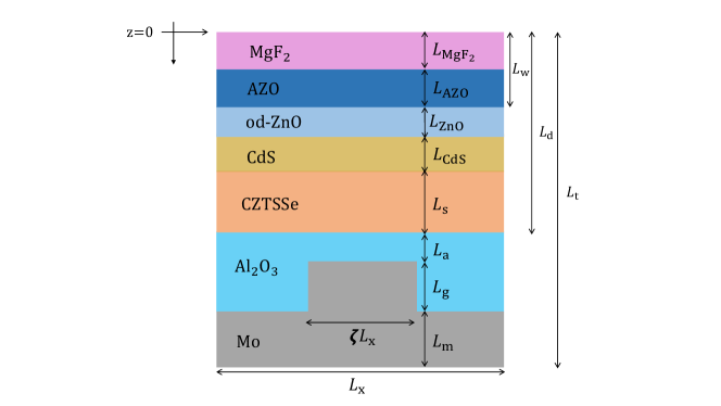
As shown in Fig. 1, we took the CZTSSe solar cell to comprise an antireflection coating of magnesium fluoride (), followed by an aluminum-doped zinc oxide (AZO) layer as the front contact, a buffer layer of oxygen-deficient zinc-oxide (od-ZnO), the ultrathin CdS layer, and the CZTSSe layer. The od-ZnO, CdS, and CZTSSe layers constitute the semiconductor region of the solar cell. Whereas the actual bandgap of CZTSSe was used for the optical part in our calculations, the bandgap was depressed in the electrical part in order to account for bandtail defects [14, 15]. The bandgap-dependent (i.e., -dependent) defect density and electron affinity were used in the electrical calculations. The nonlinear Shockley–Read–Hall (SRH) and radiative processes for electron-hole recombination were also incorporated [38, 43]. The Mo backreflector was assumed to be periodically corrugated along a fixed axis (designated as the axis) normal to the axis. A thin layer of aluminum oxide () was inserted between the CZTSSe layer and the Mo backreflector, as has been experimentally shown to prevent the formation of a Mo(SξSe1-ξ)2 layer that enhances the back-contact electron-hole recombination rate and depresses [48]. The efficiency was maximized for (a) homogeneous, (b) linearly graded, as well as (c) sinusoidally graded CZTSSe layers using the differential evolution algorithm (DEA) [49]. The role of traps at the CdS/CZTSSe interface was assessed by incorporating a surface-defect layer [50] with higher defect density.
This paper is organized as follows. The optical description of the solar cell of Fig. 1 is presented in Sec. 2.1 along with the approach taken for optical calculations. The electrical description of the solar cell is discussed in Sec 2.2. Optimization for maximum efficiency is briefly discussed in Sec. 2.3. Section 3.1 compares the efficiency of the conventional solar cell with a 2200-nm-thick homogeneous CZTSSe layer [7] with that predicted by the coupled optoelectronic model. The effects of the layer and the CdS/CZTSSe interface recombination rate on the solar-cell performance are discussed in Sec. 3.2 and Sec. 3.3, respectively. Section 3.4 provides the optimal configurations of solar cells with a homogeneous CZTSSe layer and a planar backreflector, Sec. 3.5 for solar cells with a homogeneous CZTSSe layer and a periodically corrugated backreflector, and Sec. 3.6 for solar cells with a linearly graded CZTSSe layer and either a planar or a periodically corrugated backreflector, while optimal configurations of solar cells with a sinusoidally graded CZTSSe layer and either a planar or a periodically corrugated backreflector are presented in Sec. 3.7. Concluding remarks are provided in Sec. 4.
2 Optoelectronic Modeling and Optimization
2.1 Optical theory in brief
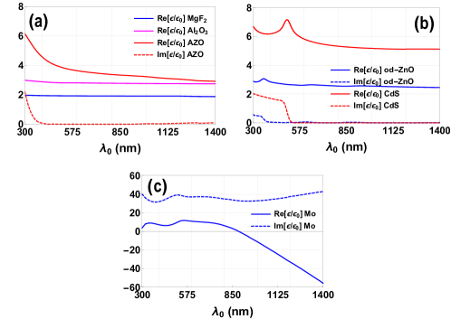
The CZTSSe solar cell occupies the region , the half spaces and being occupied by air. The reference unit cell of this structure, shown in Figure 1, occupies the region . The region nm consists of a 110-nm-thick antireflection coating [51] made of layer [52] and a 100-nm-thick AZO layer [53] as the front contact. The region is a 100-nm-thick buffer layer of oxygen-deficient zinc oxide (od-ZnO) [54]. Oxygen deficiency during the deposition of ZnO makes it an -type semiconductor [55]. The region is a 50-nm-thick layer of -type CdS [56] that forms a junction with the -type CZTSSe layer of thickness nm and a bandgap that can vary with . The region is occupied by Mo [57] of permittivity , where is the free-space wavelength. The thickness nm was chosen to be significantly larger than the electromagnetic penetration depth [58] of Mo across the visible spectrum. A thin [59] layer of thickness nm and permittivity exists between the Mo backreflector and the CZTSSe absorber layer [48].
The region has a rectangular metallic grating with period along the axis. In this region, the permittivity is given by
| (3) | |||
| (4) |
with as the duty cycle. The grating is absent for .
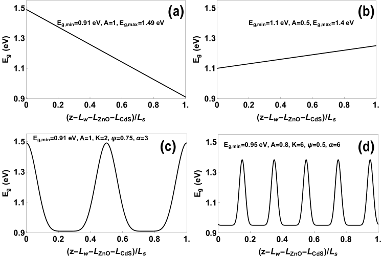
The linearly nonhomogeneous bandgap can be either backward graded or forward graded. For backward grading,
| (5) |
where is an amplitude, is the minimum bandgap, and is the maximum bandgap; represents a homogeneous CZTSSe layer. For forward grading,
| (6) |
Two representative bandgap profiles are shown in Figs. 2(a,b).
For the sinusoidally graded bandgap,
| (7) |
where the integer is the number of periods in the CZTSSe layer, describes a relative phase shift, and is a shaping parameter. Two representative profiles are provided in Figs. 2(c,d). As thin-film solar cells are fabricated using vapor-deposition techniques [60], graded bandgap profiles could be physically realized by adjusting the sulfur-to-selenium ratio in the precursor and thus varying the composition parameter during the deposition process [61, 27, 28]. Optical spectra of the relative permittivities of all materials used in the solar cell are provided in Appendix A.
The RCWA [40, 41] was used for monochromatic calculations. The electric field phasor and the magnetic field phasor , created everywhere inside the solar cell due to illumination by an unpolarized plane wave normally incident on the plane , were calculated with V m-1 being the amplitude of the incident electric field. The region was partitioned into a sufficiently large number of slices along the axis, in order to implement the RCWA. Although each slice was homogeneous along the axis, it could be periodically nonhomogeneous along the axis. The slice thickness was chosen by trial and error such that the useful solar absorptance [62] converged with a preset tolerance of . The usual boundary conditions on the continuity of the tangential components of the electric and magnetic field phasors were enforced on the plane to match the internal field phasors to the sum of the incident and reflected field phasors. The same was done to match the internal field phasors to the transmitted field phasors on the plane . Detailed descriptions of the RCWA for solar cells are available [62, 41, 63].
Suppose that every photon absorbed in the semiconductor region excites an electron-hole pair. Then, the -averaged electron-hole-pair generation rate is [26]
| (8) |
for , where is the reduced Planck constant, is the free-space permittivity, is the free-space permeability, is the AM1.5G solar spectrum [42], nm, and nm with stated in eV. Averaging about the axis can be justified for two reasons. First, any current generated parallel to the axis shall be negligibly small because the solar cell operates under the influence of a -directed electrostatic field due to the application of . Second, for electrostatic analysis 500 nm is very small in comparison to the lateral dimensions of the solar cell.
2.2 Electrical theory in brief
For electrical modeling, only the region has to be considered, because electron-hole pair generation occurs in the CZTSSe, od-ZnO, and CdS layers only. With a bandgap of 3.3 eV, od-ZnO absorbs solar photons with energies corresponding to nm. Likewise, CdS absorbs solar photons with energies corresponding to nm, as its bandgap is 2.4 eV. The planes and were assumed to be ideal ohmic contacts, as we are not interested in how the solar cell interacts with an external circuit.
The electron quasi-Fermi level
| (9) |
and the hole quasi-Fermi level
| (10) |
depend on as the density of states in the conduction band, as the density of states in the valence band, as the conduction band-edge energy, as the valence band-edge energy, as the dc electric potential, as the bandgap-dependent electron affinity, as the Boltzmann constant, and as the absolute temperature. The reference energy level is arbitrary.
The gradients of the quasi-Fermi levels drive the the electron-current density and the hole-current density ; thus,
| (11) |
where 10-19 C is the charge quantum, is the electron density, is the hole density, is the electron mobility, and is the hole mobility. According to the Boltzmann approximation [43],
| (12) |
where
| (13) |
is the intrinsic charge-carrier density and
| (14) |
is the intrinsic energy. Both and are functions of because they depend on the bandgap but we took them to be independent of , following Hironiwa et al. [32], because bandgap-dependent values are unavailable for CZTSSe.
The 1D drift-diffusion model comprises the three differential equations [43, Sec. 4.6]
| (15) |
under steady-state conditions, with as the electron-hole-pair recombination rate, as the defect density or the trap density, is the doping density which is positive for donors and negative for acceptors, and as the dc relative permittivity. Both and depend on and, therefore, on . All three differential equations have to be solved simultaneously for .
The radiative recombination rate is given by
| (16) |
where is the radiative recombination coefficient [43, 38]. The SRH recombination rate is given by
| (17) |
where is the electron density and is the hole density at the trap energy level ; the electron lifetime depends on the electron-capture cross section , the hole lifetime depends on the hole-capture cross section , and is the mean thermal speed of all charge carriers [43, 38]. The total recombination rate then is .
Dirichlet boundary conditions on , , and at the planes and supplement Eqs. (15) [63, 39]. These boundary conditions were derived after assuming the region to be charge-free and in local quasi-thermal equilibrium [38]. The bias voltage was taken to be applied at the plane .
The HDG scheme [64, 45, 46] was used to solve all three differential equations. This scheme works well for solar cells containing heterojunction interfaces [47]. All -dependent variables are discretized in this scheme using discontinuous finite elements in a space of piecewise polynomials of a fixed degree. We used the Newton–Raphson method to solve the resulting system for , , and [65].
Table I provides the values of electrical parameters used for od-ZnO, CdS, and CZTSSe [66, 6, 12]. The effect of bandtail states, which effectively narrow the bandgap, was incorporated [14, 15] by reducing the bandgap of CZTSSe for electrical calculations. Whereas eV was used for CZTSSe in the optical part of the coupled optoelectronic model, eV was used in the electrical part [15, 14].
| Symbol (unit) | od-ZnO [66] | CdS [66] | CZTSSe [6, 12] |
|---|---|---|---|
| (eV) | 3.3 | 2.4 | (optical part) |
| (electrical part)† | |||
| (eV) | 4.4 | 4.2 | |
| (cm-3) | 1 (donor) | 5 (donor) | 1 (acceptor) |
| (cm-3) | |||
| (cm-3) | |||
| (cm2 V-1 s-1) | 40 | ||
| (cm2 V-1 s-1) | 31 | 12.6 | |
| 9 | 5.4 | ||
| (cm-3) | |||
| midgap | midgap | midgap | |
| (cm2) | |||
| (cm2) | |||
| (cm3 s-1) | |||
| (cm s-1) |
† is artificially reduced in the electrical part so as to account for bandtail states.
2.3 Optoelectronic optimization
The total current density equals everywhere in the od-ZnO, CdS, and CZTSSe layers, under steady-state conditions. When the solar cell is connected to an external circuit, is the current density delivered by the former to the latter. The short-circuit current density is the value of when and the open-circuit voltage is the value of such that . The power density is defined as ; the maximum power density obtainable from the solar cell is the highest value of on the - curve; and , where W m-2 is the integral of over the solar spectrum. The fill factor is commonly encountered in the solar-cell literature.
The DEA [49] was used to optimize with respect to certain geometric and bandgap parameters, using a custom algorithm implemented with MATLAB® version R2017b.
3 Numerical results and discussion
3.1 Conventional CZTSSe solar cell (model validation)
Our coupled optoelectronic model was validated by comparison with experimental results available for the conventional /AZO/od-ZnO/CdS/CZTSSe/Mo(SξSe1-ξ)2/Mo solar cell containing a 2000-nm-thick homogeneous CZTSSe layer and a planar backreflector [7]. In this solar cell, a 200-nm-thick Mo(SξSe1-ξ)2 layer with defect density cm-3 is present whereas the layer is absent in relation to Fig. 1, and we made appropriate modifications for the validation. All other relevant electrical parameters of Mo(SξSe1-ξ)2 were taken to be the same as that of CZTSSe, except that eV [67] was used for Mo(SξSe1-ξ)2 in both the optical and electric parts of the coupled optoelectronic model. The relative permittivity of Mo(SξSe1-ξ)2 in the optical regime is provided in Appendix A.
The values of , , , and obtained from our coupled optoelectronic model for are provided in Table II along with the corresponding experimental data [19, 7, 15]. According to this table, the model’s predictions are in reasonable agreement with the experimental data, the variances being very likely due to differences between the optical and electrical properties inputted to the model from those realized in practice. As interface defects are not explicitly considered in our model, all the experimentally observed features can be adequately accounted for by the bulk properties of CZTSSe, which is also in accord with the empirical model provided by Gokmen et al. [68].
In order to further elaborate the role of the Mo(SξSe1-ξ)2 layer, we lowered its thickness from nm to nm but increased the thickness of the CZTSSe absorber layer from nm to nm. The composition parameter was taken to be for the Mo(SξSe1-ξ)2 layer as well as for the CZTSSe layer, but other parameters remained the same as for the model’s results stated in Table II. The model-predicted efficiency increased from to , indicating the minor role of the thickness of the Mo(SξSe1-ξ)2 layer.
| (mA cm-2) | (mV) | (%) | (%) | ||
| 0 | Model | 38.31 | 361 | 65 | 8.96 |
| Experiment | |||||
| (Ref. 19) | 36.4 | 412 | 62 | 9.33 | |
| 0.38 | Model | 32.42 | 509 | 69 | 11.15 |
| Experiment | |||||
| (Ref. 7) | 35.2 | 513.4 | 69.8 | 12.6 | |
| 1 | Model | 17.86 | 606 | 60.7 | 6.61 |
| Experiment | |||||
| (Ref. 15) | 16.9 | 637 | 61.7 | 6.7 |
3.2 Effect of layer
The incorporation of an ultrathin layer below the CZTSSe layer prevents the formation of a Mo(SξSe1-ξ)2 layer and thereby enhances performance [48]. Removing the Mo(SξSe1-ξ)2 layer and reverting to the solar cell depicted in Fig. 1, we optimized the CZTSSe solar cell with and without a -nm-thick layer between the CZTSSe layer and a planar Mo backreflector.
Values of , , , and obtained from our coupled optoelectronic model for nm are presented in Table III. The optimal efficiency is % with the layer and % without it. Thus, the layer enhances slightly, and concurrent improvements in both and can also be noted in Table III. Hence, the 20-nm-thick layer was incorporated in the solar cell for all of the following results.
| (nm) | (mA cm-2) | (mV) | (%) | (%) | |
| 0 | 0.50 | 29.51 | 552 | 69.70 | 11.37 |
| 20 | 0.50 | 30.00 | 557 | 70.31 | 11.76 |
3.3 Effect of surface recombination on CdS/CZTSSe interface
A 10-nm-thin surface-defect layer was inserted between the CdS and CZTSSe layers to investigate the effect of surface recombination at that interface on the performance of the solar cell depicted in Fig. 1. The CZTSSe layer was taken to be homogeneous with thickness nm and all other parameters as reported in Table I. The surface defect density was fixed at cm-2 but the mean thermal speed was varied between cm s-1 and cm s-1 in the surface-defect layer, with all other characteristics of this layer taken to be the same as of the CZTSSe layer.
The optimal value of for nm. On inserting the surface-defect layer, the efficiency reduced from % to: (i) % when cm s-1 in the surface-defect layer and (ii) % when is 107 cm s-1 in the surface-defect layer. The optimal value of for nm. On inserting the surface-defect layer, the efficiency reduced from % to: (i) % when cm s-1 in the surface-defect layer and (ii) % when is 107 cm s-1 in the surface-defect layer. Similar efficiency reductions were predicted for intermediate values of . These efficiency reductions are so small that the surface-defect layer can be ignored with minimal consequences. Therefore, we neglected surface recombination on the CdS/CZTSSe interface for all results presented from now onwards.
3.4 Optimal solar cell: Homogeneous bandgap & planar backreflector
Next, we optimized a solar cell in which the CZTSSe layer is homogeneous () and the backreflector is planar (), in order to highlight the advantage of the nonhomogeneous CZTSSe layer.
For a fixed value of , the parameter space for optimizing is: eV (for the optical part***Throughout Sec. 3, the values of stated for the CZTSSe layer pertain to the optical part of the coupled optoelectronic model. Knowing for the optical part, one can use Table I to find and, therefore, for the electrical part of the coupled optoelectronic model. ). With nm, the maximum efficiency predicted for and is when eV. The corresponding values of , , and are mA cm-2, mV, and , respectively. Incidentally, the efficiency becomes lower for eV because of
-
(a)
the narrowing of the portion of the solar spectrum available for photon absorption [69] due to the blue shift of , and
- (b)
Next, we considered nm also as a parameter for maximizing . The highest efficiency predicted is , produced by a solar cell with a 1200-nm-thick CZTSSe layer with an optimal bandgap of eV. The values of , , and corresponding to this optimal design are mA cm-2, mV, and %, respectively.
In order to compare the performance of the solar cell with optimal , values of (for the optical part), , , , and predicted by the coupled optoelectronic model are presented in Table IV for seven representative values of . The maximum efficiency increases to 11.84% as increases to 1200 nm, but decreases at a very slow rate with further increase of . The efficiency increase with for nm is due to the increase in volume available to absorb photons. The efficiency reduction for nm is due to reduced charge-carrier collection arising from short diffusion length of minority charge carriers in CZTSSe being smaller than [18]. Notably, the optimal bandgap of the CZTSSe layer fluctuates in a small range (i.e., eV), despite a -fold increase of .
| (nm) | (eV) | (mA cm-2) | (mV) | (%) | (%) |
| 100 | 1.21 | 19.23 | 513 | 75.2 | 7.41 |
| 200 | 1.20 | 25.19 | 535 | 72.0 | 9.67 |
| 300 | 1.20 | 27.27 | 546 | 69.6 | 10.38 |
| 400 | 1.20 | 28.07 | 551 | 69.6 | 10.79 |
| 600 | 1.18 | 29.31 | 556 | 70.0 | 11.47 |
| 1200 | 1.21 | 30.13 | 558 | 70.3 | 11.84 |
| 2200 | 1.20 | 30.00 | 557 | 70.3 | 11.76 |
3.5 Optimal solar cell: Homogeneous bandgap & periodically corrugated backreflector
Next, we carried out the optoelectronic optimization of solar cells with a homogeneous CZTSSe layer (), as in Sec. 3.4, but with a periodically corrugated backreflector. The parameter space for optimizing was set up as: nm, eV for the optical part, nm, , and nm.
The values of , , , and predicted by the coupled optoelectronic model are presented in Table V for seven representative values of . The values of , , and for the optimal designs are also provided in the same table.
On comparing Tables IV and V, we found that periodic corrugation of the Mo backreflector slightly improves for nm. For example, relative to the planar backreflector, the efficiency increases from to when nm, the other parameters being nm, , nm, and eV. No improvement in efficiency was found for nm by the use of a periodically corrugated backreflector. The optimal bandgap of CZTSSe remains the same as with the planar backreflector in Sec. 3.4; also, the optimal corrugation parameters lie in narrow ranges: nm, , and nm.
| (nm) | (eV) | (nm) | (nm) | (mA cm-2) | (mV) | (%) | (%) | |
| 100 | 1.21 | 100 | 0.50 | 500 | 19.99 | 506 | 75.2 | 7.62 |
| 200 | 1.20 | 105 | 0.51 | 510 | 25.34 | 532 | 72.3 | 9.75 |
| 300 | 1.20 | 100 | 0.50 | 500 | 27.87 | 546 | 70.4 | 10.72 |
| 400 | 1.19 | 103 | 0.51 | 502 | 28.56 | 547 | 69.7 | 10.91 |
| 600 | 1.18 | 99 | 0.50 | 508 | 29.43 | 556 | 70.2 | 11.50 |
| 1200 | 1.21 | 101 | 0.51 | 500 | 30.13 | 558 | 70.3 | 11.84 |
| 2200 | 1.20 | 100 | 0.50 | 500 | 30.00 | 557 | 70.3 | 11.76 |
3.6 Optimal solar cell: Linearly graded bandgap and planar/periodically corrugated backreflector
Next, we considered the maximization of when the bandgap of the CZTSSe layer is linearly graded, according to either Eq. (5) or Eq. (6), and the backreflector is either planar or periodically corrugated.
3.6.1 Backward grading
Equation (5) is used for backward grading, i.e., the bandgap near the front contact is larger than the bandgap near the back contact for . Optoelectronic optimization yielded , i.e., a homogeneous bandgap, whether the backreflector is planar or periodically corrugated. Therefore, the optimized results provided in Secs. 3.4 and 3.5 also apply for backward bandgap grading of the CZTSSe layer.
3.6.2 Forward grading
On the other hand, when Eq. (6) is used, the bandgap near the front contact is smaller than the bandgap near the back contact for . The parameter space used for optimizing is: nm, eV, eV, , nm, , and nm with the condition that . The values of , , , and predicted by the coupled optoelectronic model are presented in Table VI for seven representative values of . The values of , , , , and for the optimal designs are also provided in the same table. The corresponding data for optimal solar cells with a planar backreflector () are provided for comparison in Table VII.
Just as in Sec. 3.5, on comparing Tables VI and VII, we found that periodic corrugation of the Mo backreflector slightly improves for nm. Thus, for nm, the maximum efficiency predicted is % with a planar backreflector and % with a periodically corrugated backreflector. Whether the backreflector is planar or periodically corrugated, the optimal parameters for forward grading are: eV, eV, and . The optimal parameters for the periodically corrugated backreflector for nm are: nm, , and nm. No improvement in efficiency was found for nm by the use of a periodically corrugated backreflector.
The highest efficiency predicted in Tables VI and VII is %, which arises when nm, eV, eV, and for both planar () and periodically corrugated backreflectors. The values of , , and corresponding to this optimal design are mA cm-2, mV, and , respectively. Relative to the optimal homogeneous CZTSSe layer (Sec. 3.4), the maximum efficiency increases from to (a relative increase of ) with forward grading of the CZTSSe layer; concurrently, , , as well as are also enhanced.
The optimal values of eV and in Tables VI and VII, and the optimal values of are independent of , whether the backreflector is planar or periodically corrugated. Also, the optimal corrugation parameters are very weakly dependent on : nm, , and nm.
| (nm) | (eV) | (eV) | (nm) | (nm) | (mA cm-2) | (mV) | (%) | (%) | ||
| 100 | 0.92 | 1.49 | 0.99 | 100 | 0.50 | 510 | 20.24 | 544 | 76.0 | 8.44 |
| 200 | 0.92 | 1.49 | 1.00 | 100 | 0.50 | 500 | 27.42 | 572 | 74.5 | 11.69 |
| 300 | 0.91 | 1.49 | 0.99 | 100 | 0.50 | 510 | 29.88 | 592 | 74.0 | 13.01 |
| 400 | 0.92 | 1.49 | 0.99 | 100 | 0.51 | 550 | 31.39 | 603 | 73.0 | 13.91 |
| 600 | 0.91 | 1.49 | 1.00 | 100 | 0.50 | 502 | 32.98 | 612 | 73.6 | 14.87 |
| 1200 | 0.93 | 1.49 | 0.99 | 100 | 0.51 | 500 | 35.02 | 617 | 73.5 | 15.90 |
| 2200 | 0.91 | 1.49 | 0.99 | 100 | 0.51 | 500 | 36.72 | 628 | 74.0 | 17.07 |
| (nm) | (eV) | (eV) | (mA cm-2) | (mV) | (%) | (%) | |
| 100 | 0.91 | 1.49 | 0.99 | 19.34 | 550 | 76.8 | 8.18 |
| 200 | 0.92 | 1.49 | 0.99 | 26.18 | 568 | 74.2 | 11.04 |
| 300 | 0.91 | 1.49 | 0.99 | 30.07 | 590 | 73.2 | 13.00 |
| 400 | 0.91 | 1.49 | 0.99 | 31.16 | 601 | 73.4 | 13.75 |
| 600 | 0.92 | 1.49 | 0.99 | 33.17 | 610 | 73.6 | 14.92 |
| 1200 | 0.93 | 1.49 | 0.99 | 35.02 | 617 | 73.5 | 15.90 |
| 2200 | 0.91 | 1.49 | 0.99 | 36.72 | 628 | 74.0 | 17.07 |
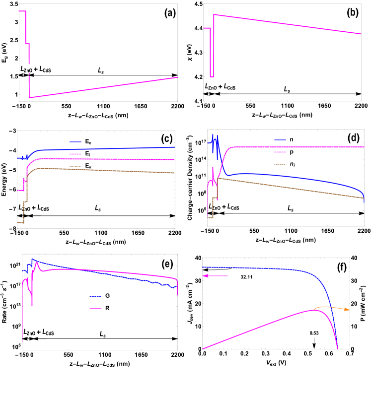
No difference could be discerned in the semiconductor regions of the forward-graded solar cells with the highest efficiency in Tables VI and VII, the CZTSSe absorber layer being -nm thick whether the backreflector is planar or periodically corrugated. Spatial profiles of and are provided in Fig. 3(a,b), whereas Fig. 3(c) presents the spatial profiles of , , and . The spatial variations of and are quasilinear, quite similar to that of . Figure 3(d) presents the spatial profiles of , , and . We note that varies linearly with such that it is small where is large and vice versa.
Spatial profiles of and are provided in Fig. 3(e). The generation rate is higher near the front face and lower near the rear face of the CZTSSe layer, which is in accord with the understanding [38, 70] that more charge carriers are generated in regions where is lower and vice versa; less energy is required to excite a charge carrier from the valence band to the conduction band when is lower. The - curve of the solar cell is shown in Fig. 3(f). From this figure, mA cm-2, V, and for best performance.
3.7 Optimal solar cell: Sinusoidally graded bandgap & planar/periodically corrugated backreflector
Finally, we considered the maximization of for solar cells with a sinusoidally graded CZTSSe layer according to Eq. (7) and a periodically corrugated backreflector. The parameter space used for optimizing is: nm, eV, , , , , nm, , and nm. The values of , , , and predicted by the coupled optoelectronic model are presented in Table VIII for eight representative values of . The values of , A, K, , , , and for the optimal designs are also provided in the same table. For comparison, the corresponding data for optimal solar cells with a planar backreflector () are provided in Table IX.
Just as in Secs. 3.5 and 3.6.2, on comparing Tables VIII and IX, we found that periodic corrugation of the Mo backreflector slightly improves for nm. For nm, the optimal efficiency predicted is with a planar backreflector (Table IX) and with a periodically corrugated backreflector (Table VIII). The optimal bandgap parameters for either backreflector are: eV, , , , and . The geometric parameters of the optimal periodically corrugated backreflector are: nm, , and nm. For nm, the optimal efficiency predicted is , regardless of the geometry of the backreflector, the optimal bandgap parameters being: eV, , , , and . Indeed, the effect of periodic corrugation remains the same as in the cases of the homogeneous bandgap (Sec. 3.5) and the linearly graded bandgap (Sec. 3.6.2): very small improvement for thin CZTSSe layers and no improvement beyond nm.
The optimal designs in Table VIII have nm, and nm. The values of eV, , , , and for both planar and periodically corrugated backreflectors.
| (nm) | (eV) | (nm) | (nm) | (mA | (mV) | (%) | (%) | |||||
| cm-2) | ||||||||||||
| 100 | 0.92 | 0.98 | 3 | 6 | 0.75 | 100 | 0.50 | 500 | 25.72 | 701 | 78.7 | 14.22 |
| 200 | 0.92 | 0.99 | 3 | 6 | 0.75 | 100 | 0.51 | 510 | 32.99 | 716 | 77.5 | 17.83 |
| 300 | 0.92 | 0.98 | 2 | 6 | 0.75 | 100 | 0.51 | 510 | 35.15 | 745 | 74.7 | 19.58 |
| 400 | 0.92 | 0.98 | 2 | 6 | 0.75 | 100 | 0.51 | 510 | 36.32 | 762 | 74.4 | 20.62 |
| 600 | 0.92 | 0.98 | 2 | 6 | 0.75 | 100 | 0.50 | 500 | 37.23 | 771 | 74.8 | 21.47 |
| 870 | 0.92 | 0.98 | 2 | 6 | 0.75 | 100 | 0.50 | 500 | 37.39 | 772 | 75.2 | 21.74 |
| 1200 | 0.92 | 0.98 | 2 | 6 | 0.75 | 100 | 0.51 | 510 | 37.08 | 766 | 74.8 | 21.26 |
| 2200 | 0.92 | 0.98 | 2 | 6 | 0.75 | 100 | 0.51 | 510 | 36.45 | 736 | 72.8 | 19.56 |
| (nm) | (eV) | (mA | (mV) | (%) | (%) | ||||
| cm-2) | |||||||||
| 100 | 0.91 | 0.99 | 3 | 6 | 0.75 | 25.65 | 703 | 78.6 | 14.19 |
| 200 | 0.92 | 0.99 | 3 | 6 | 0.75 | 32.40 | 719 | 75.0 | 17.48 |
| 300 | 0.92 | 0.98 | 2 | 6 | 0.75 | 33.94 | 744 | 75.0 | 19.01 |
| 400 | 0.92 | 0.98 | 2 | 6 | 0.75 | 35.69 | 762 | 75.0 | 20.35 |
| 600 | 0.92 | 0.98 | 2 | 6 | 0.75 | 37.17 | 771 | 74.8 | 21.46 |
| 870 | 0.92 | 0.98 | 2 | 6 | 0.75 | 37.39 | 772 | 75.2 | 21.74 |
| 1200 | 0.92 | 0.98 | 2 | 6 | 0.75 | 37.08 | 766 | 74.8 | 21.26 |
| 2200 | 0.92 | 0.98 | 2 | 6 | 0.75 | 36.45 | 736 | 72.8 | 19.56 |
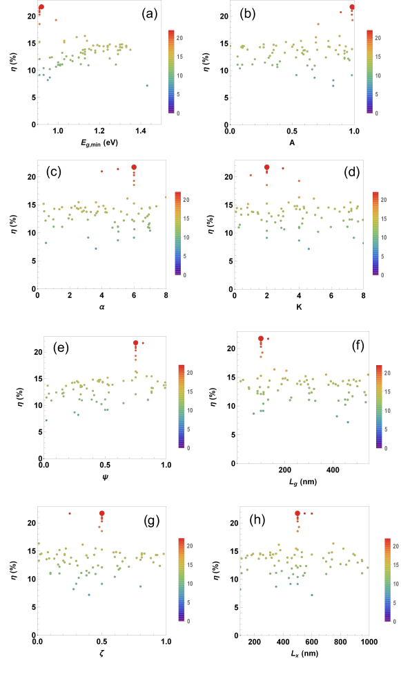
The highest efficiency achievable is predicted to be % with a sinusoidally graded CZTSSe layer of thickness nm, whether the backreflector is planar (Table IX) or periodically corrugated (Table VIII). Figure 4 shows the projections of the nine-dimensional space onto the sets of axes with the efficiency on the vertical axis and each of the optimization parameters on the horizontal axis, when nm and the backreflector is periodically corrugated. The large dots highlight the location of the solar cell with the maximum efficiency. The optimal combination of the values of the parameters , , , ,, , , and is recorded in Table VIII.
The highest possible efficiency () with a sinusoidally graded CZTSSe layer amounts to a relative increase of over the optimal efficiency of with a homogeneous CZTSSe layer of thickness nm (Secs. 3.4 and 3.5). Along with the increase in efficiency, increases from mA cm-2 to mA cm-2 (a relative increase of ), from mV to mV (a relative increase of ), and from to (a relative increase of ).
The highest possible efficiency () with a sinusoidally graded CZTSSe layer is higher than the highest possible efficiency () with a linearly graded CZTSSe layer (Sec. 3.6.2). The short-circuit current density for sinusoidal grading is somewhat higher as well, but the open-circuit voltage is enhanced considerably from mV to mV. Let us note, however, that the optimal sinusoidally graded CZTSSe layer is only -nm thick, but its optimal linearly graded counterpart is -nm thick. Indeed, the sinusoidally graded bandgap is more efficient than the homogeneous and linearly graded bandgaps for all considered thicknesses of the CZTSSe layer.
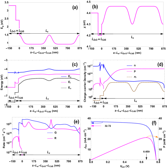
The variations of and with in the semiconductor region of the solar cell with the optimal sinusoidally graded -nm-thick CZTSSe layer are provided in Fig. 5(a,b). With eV and , eV. The magnitude of is large near both faces of the CZTSSe layer, which elevates [28]. Furthermore, bandgap grading in the proximity of the rear face of the CZTSSe layer keeps the minority carriers away from that face (where recombination would be highly favored in the absence of the layer [48]) to reduce recombination [71] and improve the carrier collection due to the drift field provided by the bandgap grading [72]. The regions in which is small are of substantial thickness, and it is those very regions that are responsible for increasing the electron-hole-pair generation rate [38, 70], because less energy is required to excite an electron-hole pair across a narrower bandgap. Thus, this bandgap profile is ideal for the enhancement of while maintaining a large .
Figure 5(c) shows the variations of , , and with respect to . The spatial profiles of and are similar to that of . Figure 5(d) shows the spatial variations of , , and under equilibrium; specifically, varies such that it is large where is small and vice versa. The spatial profiles of and are shown in Fig. 5(e). Specifically, is higher in regions with lower and vice versa, as discussed for Fig. 5(a). The higher recombination rate in the -nm-thick middle region is due to higher defect/trap density caused by higher sulfur content. The - characteristics are shown in Fig. 5(f). Our optoelectronic model predicts mA cm-2, V, and % for best performance.
4 Concluding remarks
We implemented a coupled optoelectronic model along with the differential evolution algorithm to assess the efficacy of grading the bandgap of the CZTSSe layer for enhancing the power conversion efficiency of thin-film CZTSSe solar cells. Both linearly and sinusoidally graded bandgaps were examined, with the Mo backreflector in the solar cell being either planar or periodically corrugated.
An -nm-thick sinusoidally graded CZTSSe layer accompanied by a periodically corrugated backreflector delivers a % efficiency, mA cm-2 short-circuit current density, mV open-circuit voltage, and % fill factor. Even if the backreflector is flattened, these quantities do not alter. In comparison, %, mA cm-2, mV, and %, when the bandgap is homogeneous and the backreflector is planar. Efficiency can also be enhanced by linearly grading the bandgap, but the gain is smaller compared to the case of sinusoidal bandgap grading.
The generation rate is higher in the broad small-bandgap regions than elsewhere in the CZTSSe layer, when the bandgap is sinusoidally graded. Since the bandgap is high close to both faces of the CZTSSe layer, is high in the optimal designs [28, 20]. Both of these features are responsible of enhancing .
The placement of an ultrathin layer behind the rear face of the CZTSSe layer helps remove an unwanted Mo(SξSe1-ξ)2 layer and slightly enhances the efficiency. Furthermore, for a thin CZTSSe layer ( nm), periodically corrugating the backreflector can also provide small gains over a planar backreflector.
Optoelectronic optimization thus indicates that % efficiency can be achieved for CZTSSe solar cell with a -nm-thick CZTSSe layer. This efficiency significantly higher compared to % efficiency demonstrated with CZTSSe layers that are more than two times thicker. Efficiency enhancements of comparable magnitude—e.g., to —have been predicted by bandgap grading of the CIGS layer in thin-film CIGS solar cells [26] (which, however, use some materials that are not known to be abundant on Earth). Thus, bandgap grading can provide a way to realize more efficient thin-film solar cells for ubiquitous small-scale harnessing of solar energy.
Appendix A Relative permittivities of materials in the optical regime
Spectra of the real and imaginary parts of the relative permittivity
of [52], AZO [53], od-ZnO [54], CdS [56],
Mo [57], and [59] in the optical regime are displayed in Fig. 6.
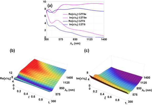
Spectra of the real and imaginary parts of the relative permittivity
of CZTS and CZTSe are available [6]. These
were incorporated in an energy-shift model [73, 36]
to obtain the relative permittivity of CZTSSe
as a function of (and, therefore, the bandgap )
and in the optical regime, as shown in Fig. 7.
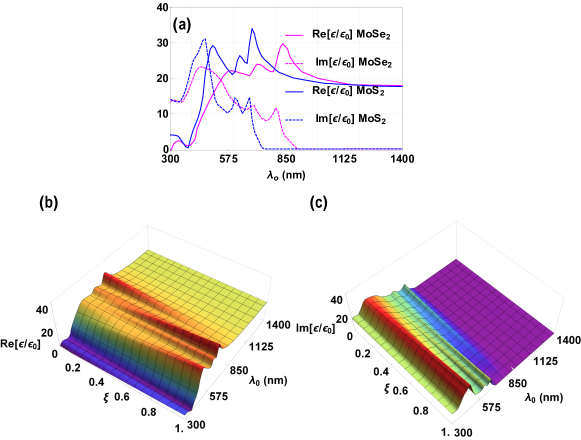
Spectra of the real and imaginary parts of the relative permittivity
of MoS2 and MoSe2 are available
for nm [67]. These were first linearly extrapolated for
nm and
then incorporated in the energy-shift model [73, 36]
to obtain the relative permittivity of Mo(SξSe1-ξ)2
as a function of
and , as shown in Fig. 8.
Acknowledgments. The authors thank anonymous reviewers for invaluable suggestions to improve the contents of this paper. A. Lakhtakia acknowledges the Charles Godfrey Binder Endowment at the Pennsylvania State University and the Otto Mønsted Foundation in Frederiksberg, Denmark for partial support. The research of F. Ahmed and A. Lakhtakia was partially supported by US National Science Foundation (NSF) under grant number DMS-1619901. The research of T.H. Anderson and P.B. Monk was partially supported by the US National Science Foundation (NSF) under grant number DMS-1619904.
References
- [1] Singh R, Alapatt G F and Lakhtakia A 2013 IEEE J. Electron Dev. Soc. 1 129–144
- [2] Dudley D 2019 Renewable Energy Costs Take Another Tumble, Making Fossil Fuels Look More Expensive Than Ever (accessed 05 July 2019)
- [3] Singh R, Alapatt G F and Bedi G 2014 Facta Universitatis: Electron. Energetics 27 275–298
- [4] Lee T D and Ebong A U 2017 Renew. and Sustain. Energ. Reviews 70 1286–1297
- [5] Candelise C, Winskel M and Gross R 2012 Prog. Photovolt: Res. Appl. 20 816–831
- [6] Adachi S 2015 Earth-Abundant Materials for Solar Cells: Cu2-II-IV-VI4 Semiconductors (Chichester, West Sussex, UK: Wiley)
- [7] Wang W, Winkler M T, Gunawan O, Gokmen T, Todorov T K, Zhu Y and Mitzi D B 2014 Adv. Energy Mater. 4 1301465
- [8] Wong L H, Zakutayev A, Major J D, Hao X, Walsh A, Todorov T K and Saucedo E 2019 J. Phys. Energy 1 032001
- [9] Jackson P, Wuerz R, Hariskos D, Lotter E, Witte W and Powalla M 2016 Phys. Stat. Sol. RRL 10 583–586
- [10] Green M A, Hishikawa Y, Dunlop E D, Levi D H, Hohl-Ebinger J and Ho-Baillie A W Y 2018 Prog. Photovolt.: Res. Appl. 26 427-436
- [11] Gershon T, Gokmen T, Gunawan O, Haight R, Guha S and Shin B 2014 MRS Commun. 4 159–170
- [12] Kanevce A, Repins I and Wei S H 2015 Sol. Energy Mater. Sol. Cells 133 119–125
- [13] Lee Y S, Gershon T, Gunawan O, Todorov T K, Gokman T, Virgus Y and Guha S 2015 Adv. Energy Mater. 5 1401372
- [14] Gokmen T, Gunawan O, Todorov T K and Mitzi D B 2013 Appl. Phys. Lett. 103 103506
- [15] Frisk C, Ericson T, Li S-Y, Szaniawski P, Olsson J and Platzer-Bjø̈rkman C 2016 Sol. Energy Mater. Sol. Cells 144 364–370
- [16] Repins I L, Moutinho H, Choi S G, Kanevce A, Kuciauskas D, Dippo P, Beall C L, Carapella J, DeHart C, Huang B and Wei S H 2013 J. Appl. Phys. 114 084507
- [17] Gunawan O, Todorov T K and Mitzi D B 2010 Appl. Phys. Lett. 97 233506
- [18] Gokmen T, Gunawan O and Mitzi D B 2013 J. Appl. Phys. 114 114511
- [19] Mitzi D B, Gunawan O, Todorov T K, Wang K and Guha S 2011 Sol. Energy Mater. Sol. Cells 95 1421–1436
- [20] Gloeckler M and Sites J R 2005 J. Appl. Phys. 98 103703
- [21] Schmid M 2017 Semicond. Sci. Technol. 32 043003
- [22] van Lare C, Yin G, Polman A, and Schmid M 2015 ACS Nano 9 9603–9613
- [23] Goffard J, Colin C, Mollica F, Cattoni A, Sauvan C, Lalanne P, Guillemoles J-F, Naghavi N and Collin S 2017 IEEE J. Photovolt. 7 1433–1441
- [24] Vermang B, Wätjen J T, Fjällström V, Rostvall F, Edoff M, Kotipalli R, Henry F and Flandre D 2014 Prog. Photovolt: Res. Appl. 22 1023–1029
- [25] Ahmad F, Anderson T H, Monk P B and Lakhtakia A 2018 Proc. SPIE 10731 107310L
- [26] Ahmad F, Anderson T H, Monk P B and Lakhtakia A 2019 Appl. Opt. 58 6067–6078
- [27] Woo K, Kim Y, Yang W, Kim K, Kim I, Oh Y, Kim J Y and Moon J 2013 Sci. Rep. 3 03069
- [28] Yang K-J, Son D-H, Sung S-J, Sim J-H, Kim Y-I, Park S-N, Jeon D-H, Kim J, Hwang D-K, Jeon C-W, Nam D, Cheong H, Kang J-K and Kim D-H 2016 J. Mater. Chem. A 4 10151
- [29] Hwang D-K, Ko B-S, Jeon D-H, Kang J-K, Sung S-J, Yang K-J, Nam D, Cho S, Cheong H and Kim D-H 2017 Sol. Energy Mater. Sol. Cells 161 162–169
- [30] Ferhati H and Djeffal F 2018 Opt. Mater. 76 393–399
- [31] Mohammadnejad S and Parashkouh A B 2017 Appl. Phys. A 123 758
- [32] Hironiwa D, Murata M, Ashida N, Tang Z and Minemoto T 2014 Jpn. J. Appl. Phys. 53 071201
- [33] Simya O K, Mahaboobbatcha A and Balachander K 2016 Superlattices Microstruct. 92 285–293
- [34] Chadel M, Chadel A, Bouzaki M M, Aillerie M, Benyoucef B and Charles J-P 2017 Mater. Res. Express 4 115503
- [35] Bag S, Gunawan O, Gokmen T, Zhu Y, Todorov T K and Mitzi D B 2012 Energy Environ. Sci. 5 7060
- [36] Nakane A, Tampo H, Tamakoshi M, Fujimoto S, Kim K M, Kim S, Shibata H, Niki S and Fujiwara H 2016 J. Appl. Phys. 120 064505
- [37] Burgelman M and Marlein J 2008 Proceedings of 23rd European Photovoltaic Solar Energy Conference, pp. 2151–2155, Valencia, Spain, September 1–5; doi: 10.4229/23rdEUPVSEC2008-3DO.5.2
- [38] Fonash S J 2010 Solar Cell Device Physics, 2nd ed. (Burlington, MA, USA: Academic Press)
- [39] Anderson T H, Civiletti B J, Monk P B and Lakhtakia A 2020 J. Comput. Phys. 407 109242
- [40] Glytsis E N and Gaylord T K 1987 J. Opt. Soc. Am. A 4 2061–2080
- [41] Polo Jr J A, Mackay T G and Lakhtakia A 2013 Electromagnetic Surface Waves: A Modern Perspective (Waltham, MA, USA: Elsevier)
- [42] National Renewable Energy Laboratory, Reference Solar Spectral Irradiance: Air Mass 1.5 (accessed 05 June 2019).
- [43] Nelson J 2003 The Physics of Solar Cells (London, UK: Imperial College Press)
- [44] Lehrenfeld C 2010 Hybrid Discontinuous Galerkin Methods for Solving Incompressible Flow Problems Diplomingenieur Thesis (Rheinisch-Westfaälischen Technischen Hochschule Aachen)
- [45] Cockburn B, Gopalakrishnan J and Lazarov R 2009 SIAM J. Numer. Anal. 47 1319–1365
- [46] Fu G, Qiu W and Zhang W 2015 ESAIM: Math. Model. Numer. Anal. 49 225–256
- [47] Brinkman D, Fellner K, Markowich P and Wolfram M-T 2013 Math. Models Methods Appl. Sci. 23 839–872
- [48] Liu F, Huang J, Sun K, Yan C, Shen Y, Park J, Pu A, Zhou F, Liu X, Stride J A, Green M A and Hao X 2017 NPG Asia Mater. 9 e401
- [49] Storn R and Price K 1997 J. Global Optim. 11 341–359
- [50] Song J, Li S S, Huang C H, Crisalle O D and Anderson T J 2004 Solid-State Electron. 48 73–79
- [51] Rajan G, Aryal K, Ashrafee T, Karki S, Ibdah A-R, Ranjan V, Collins R W and Marsillac S 2015 Proceedings of 42nd IEEE Photovoltaics Specialist Conference, New Orleans, LA, USA, June 14–19; doi: 10.1109/PVSC.2015.7355782
- [52] Dodge M J 1984 Appl. Opt. 23 1980–1985
- [53] Ehrmann N and Reineke-Koch R 2010 Thin Solid Films 519 1475–1485
- [54] Stelling C, Singh C R, Karg M, König T A F, Thelakkat M and Retsch M 2017 Sci. Rep. 7 42530
- [55] Wellings J S, Samantilleke A P, Warren P, Heavens S N and Dharmadasa I M 2008 Semicond. Sci. Technol. 23 125003
- [56] Treharne R E, Seymour-Pierce A, Durose K, Hutchings K, Roncallo S and Lane D 2011 J. Phys.: Conf. Ser. 286 012038
- [57] Querry M R 1987 Contractor Report CRDEC-CR-88009 (accessed 08 July 2019)
- [58] Iskander M F 2012 Electromagnetic Fields and Waves (Long Grove, IL, USA: Waveland Press)
- [59] Boidin R, Halenkovic̆ T, Nazabal V, L. Benes̆ and Nĕmec P 2016 Ceramics Int. 42 1177–1182
- [60] Martín-Palma R J and Lakhtakia A 2010 Nanotechnology: A Crash Course Bellingham, WA, USA: SPIE
- [61] Wei H, Ye Z, Li M, Su Y, Yang Z and Zhang Y 2017 CrystEngComm 13 2222
- [62] Ahmad F, Anderson T H, Civiletti B J, Monk P B and Lakhtakia A 2018 J. Nanophotonics 12 016017
- [63] Anderson T H, Monk P B and Lakhtakia A 2018 J. Photon. Energy 8 034501
- [64] Chen Y, Kivisaari P, Pistol M-E and Anttu N 2016 Nanotechnology 27 435404
- [65] Brezzi F, Marini L D, Micheletti S, Pietra P, Sacco R and Wang S 2005 Handbook of Numerical Analysis: Numerical Methods for Electrodynamic Problems, Schilders W H A and ter Maten E J W (eds) (Amsterdam, The Netherlands: Elsevier) 317–441
- [66] Frisk C, Platzer-Björkman C, Olsson J, Szaniawski P, Wätjen J T, Fjällström V, Salomé P and Edoff M 2014 J. Phys. D: Appl. Phys. 47 485104
- [67] Beal A R and Hughes H P 1979 J. Phys. C: Solid State Phys. 12 881–890
- [68] Gokmen T, Gunawan O and Mitzi D B 2014 Appl. Phys. Lett. 105 033903
- [69] Shockley W and Queisser H J 1961 J. Appl. Phys. 32 510–519
- [70] Repins I, Mansfield L, Kanevce A, Jensen S A, Kuciauskas D, Glynn S, Barnes T, Metzger W, Burst J, Jiang C-S, Dippo P, Harvey S, Teeter G, Perkins C, Egaas B, Zakutayev A, Alsmeier J-H, Luky T, Korte L, Wilks R G, Bär M, Yan Y, Lany S, Zawadzki P, Park J-S and Wei S 2016 Proceedings of 43rd IEEE Photovoltaics Specialist Conference, pp. 309–314, Portland, OR, USA, June 5–10; doi: 10.1109/PVSC.2016.7749600
- [71] Dullweber T, Lundberg O, Malmström J, Bodegrd M, Stolt L, Rau U, Schock H W and Werner J H 2001 Thin Solid Films 387 11–13
- [72] Hutchby J A 1975 Appl. Phys. Lett. 26 457–459
- [73] Hirate Y, Tampo H, Minoura S, Kadowaki H, Nakane A, Kim K M, Shibata H, Niki S and Fujiwara H 2015 J. Appl. Phys. 117 015702