Silicon sensors for the CMS HGCAL upgrade:
Challenges, sensor design & electrical characterization
Abstract
The CMS detector will undergo significant improvements to face the 10-fold increase in integrated luminosity of LHC, the so-called High-Luminosity LHC, scheduled to start in 2027. This will include a completely new calorimeter in the CMS endcap regions, which should be able to withstand fluences of up to . The new High Granularity Calorimeter (HGCAL) will have unprecedented transverse and longitudinal readout and trigger segmentation that will facilitate the particle-flow approach to reconstruct electromagnetic and hadronic particle showers and their energies. In regions of low radiation, HGCAL will be equipped with small plastic scintillator tiles as active material coupled to on-tile silicon photomultipliers. In the higher radiation zone, silicon has been chosen due to its intrinsic radiation hardness. The silicon sensors will be of hexagonal shape, with three nominal thicknesses of , and , optimized for regions of different radiation levels. They will be segmented into several hundred cells with hexagonal shape of to cm2 in size, each of which is read out individually. A comprehensive campaign is in progress to converge on optimal sensor design choices and parameters, such as bulk doping, layouts and production methods. Results from full electrical sensor characterization are presented for different sensors, together with first results from an irradiation campaign of large-area silicon sensors.
1 Introduction
Between 2025 to 2027, the Long Shutdown 3 is scheduled at CERN in which an upgrade of the accelerator and the experiments will take place in view of the High Luminosity phase of the LHC (HL-LHC) [1]. The HL-LHC will provide an unprecedented instantaneous luminosity of resulting in up to a factor of ten more in terms of the integrated luminosity than the LHC programme. In order to face this challenge, the CMS experiment has decided to install a new calorimeter in the endcap regions, the so-called High Granularity Calorimeter (HGCAL) [2]. The proposed design of HGCAL uses plastic scintillator tiles as active material in regions where the maximum radiation levels correspond to a fluence of and silicon sensors in the other sections to withstand fluences of up to .
2 HGCAL Silicon Sensors Layout
HGCAL foresees to install silicon pad sensors which combine intrinsic radiation hardness with the ability to achieve the desired jet energy resolution. The sensors designed for HGCAL are planar DC-coupled hexagonal silicon sensors fabricated on 8-inch (8”) wafers. The hexagonal geometry was chosen as largest tile-able polygon which maximizes the use of the circular wafer and minimizes the ratio of periphery to surface area.
The HGCAL silicon sensors will have three different active thicknesses (, and ) optimized for regions of different expected radiation levels. Each sensor will be segmented into several hundred cells (or pads), each of which is read out individually. The size of the single cell is optimised for physics performance considerations, such as the lateral spread of electromagnetic showers, and in view of the signal over noise ratio. In the final HGCAL layout, sensors with 120 active thickness will have 432 cells each with size, while sensors with 200 and 300 active thickness will have 192 cells each with size (table 1). Sensors with smaller pad sizes are also called High-density sensors (HD), while with larger pad sizes Low-density sensors (LD).
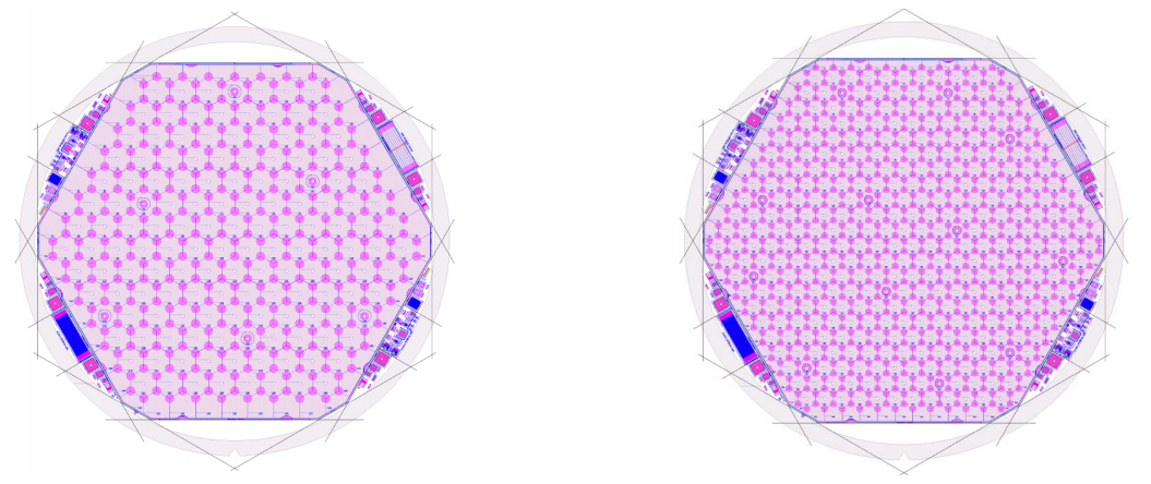
Their final layout is shown in figure 1. The corners of the sensors are truncated tips, also called mouse-bites, which allow for module mounting and further increase the use of wafer surface. In addition, two standard hexagonal cells per readout chip will have a central circular subcell, with a fourth of the area of the standard one. These dedicated low-capacitance/low-noise subcells will guarantee the ability to achieve MIP calibration even after the accumulation of the full lifetime hadron fluence of HGCAL.
Concerning the bulk polarity, p-type sensors have shown to be more robust against non-Gaussian noise present after irradiation when compared with n-type sensors by the CMS Tracker collaboration [3]. P-type epitaxial on a handle wafer is the baseline substrate material chosen for 120 sensors, while physically thinned p-type float zone silicon wafers are chosen for the sensors with larger active thicknesses. A comprehensive campaign on different non- and irradiated sensors is in progress to converge on optimal sensor design choices and parameters.
| Active thickness | Cell size | Expected range of fluence |
|---|---|---|
| [] | [] | |
| 120 | 0.52 | > 2.5 |
| 200 | 1.18 | 0.5–2.5 |
| 300 | 1.18 | 0.1–0.5 |
3 Electrical Characterisation for Sensor Prototypes
Full electrical sensor characterisation comprises studying the dependence of the leakage current, capacitance, inter-pad capacitance and resistance on the bias voltage as well as establishing the noise behaviour and charge collection efficiency on the full wafer.
For prototyping, both 6” and 8” wafers are used. Using 8” wafers have the intrinsic advantage of reducing the number of modules, and therefore of simplifying the module mechanics and minimising the production cost. On the other hand, the standard deep-diffused float zone wafer material, which is already used in several silicon detectors in high-energy particle physics experiments, is not available for these larger-area wafers. Thus, detailed studies are needed to demonstrate if the quality of the 8” production process is comparable to that of the well-established 6” one.
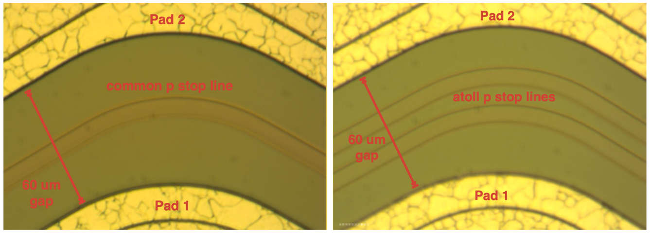
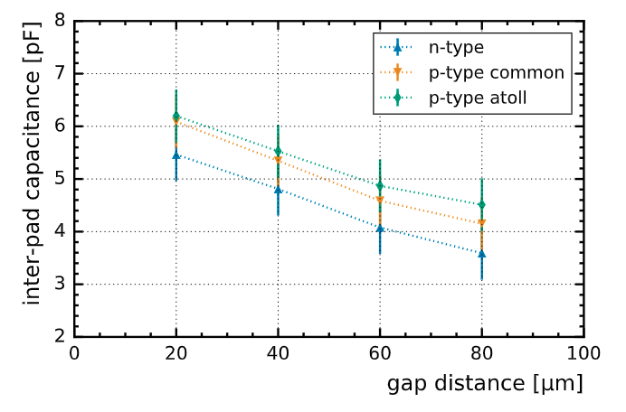
Moreover, different bulk material with n-type or p-type doping, thicknesses, distances between single pads (also called gap distances) and p-stop geometries are explored. For p-type sensors, the risk of charge-up effects on the Si-SiO2 interface is reduced by introducing additional p-implants which isolate the frontside n-implants. The two p-stop geometries considered are: ‘common’ p-stop which consists of one common grid that connects the full sensor and ‘atoll’ p-stop which consists of different independent implants that sourround each pad. They are shown in figure 2.
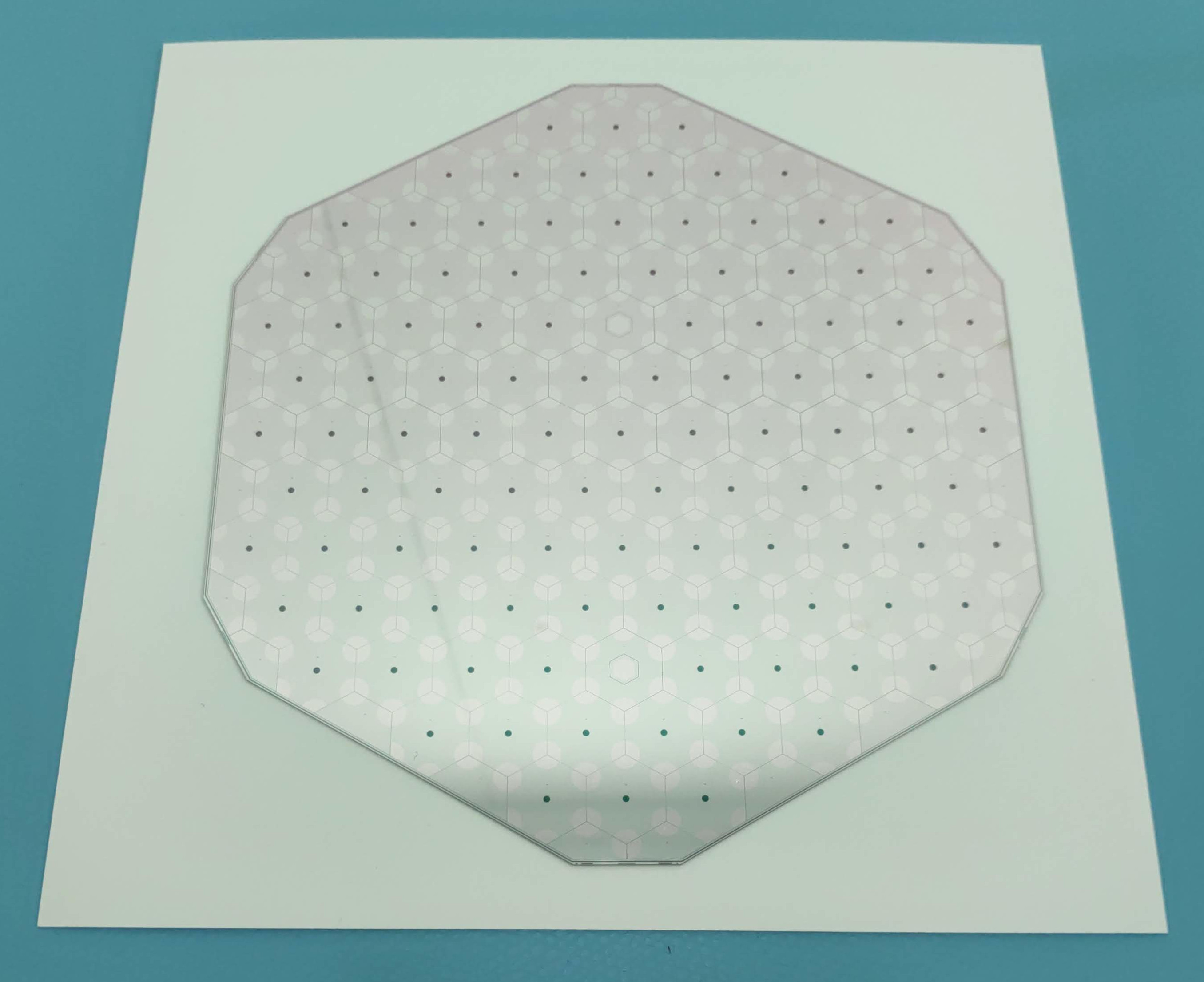
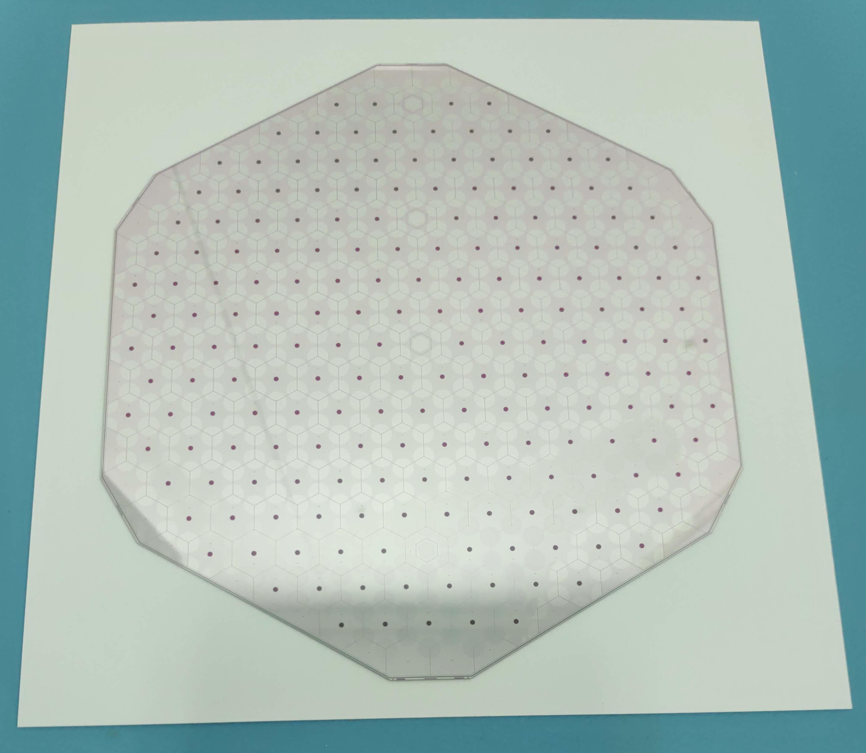
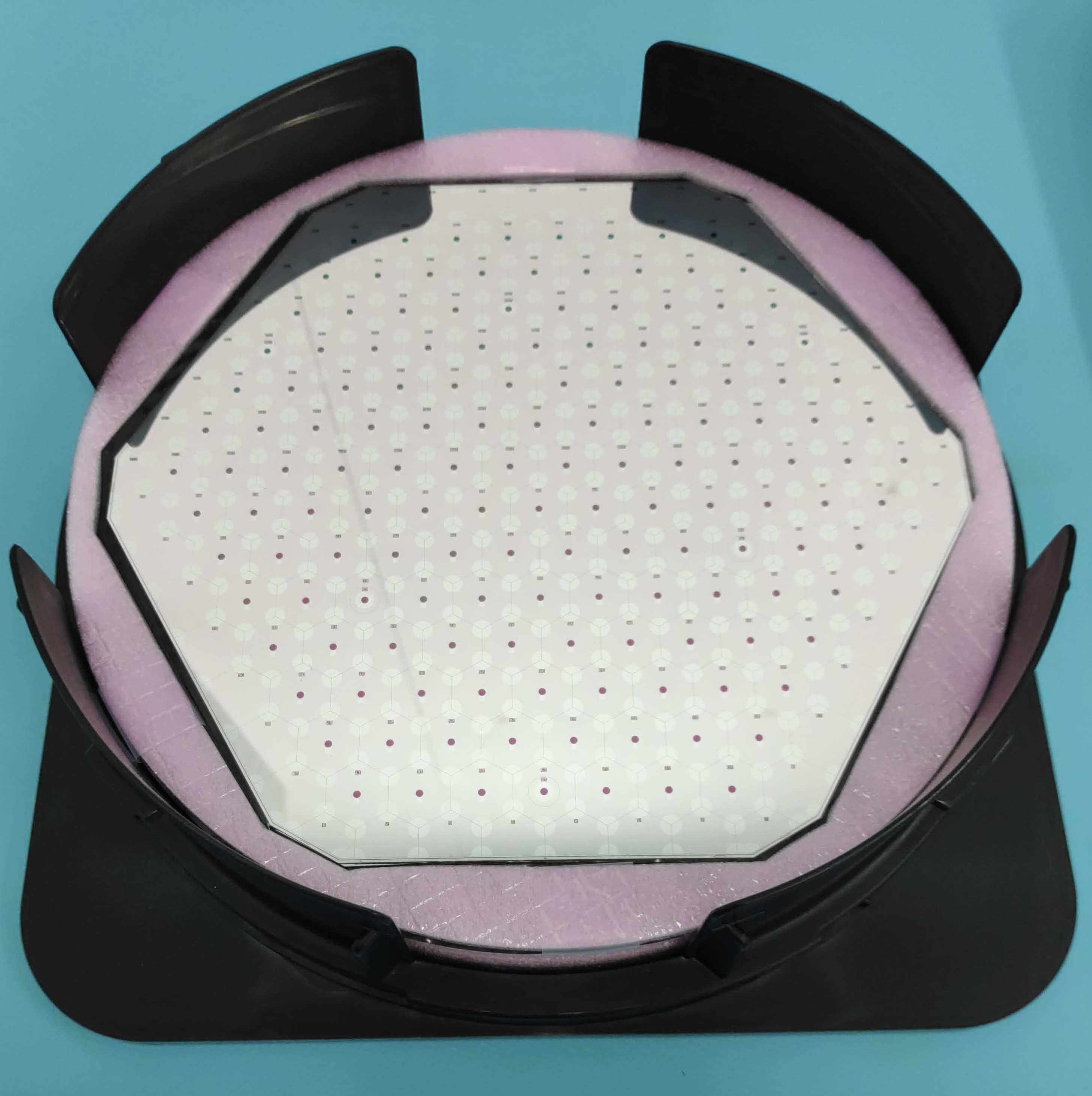
All prototypes reported in this paper as well as the final HGCAL silicon sensors are produced by Hamamatsu Photonics K.K. (HPK). A selection of full electrical sensor characterization performed on three HGCAL sensor prototypes together with first results from an irradiation campaign of large-area silicon sensors, is reported. The prototypes are shown in figure 3.
The LD 6” sensors (135-cells) have 300 active thickness and feature 20, 40, 60, and gap distances in each of four quadrants. The HD 6” sensors (239-cells) have 120 active thickness and feature 30 and gap distances. Additionally, the HD 6” sensors are equipped with several cells, so-called jumper cells, which have an extension of the metal pad to the connected area, so that four cells can be connected to the module in the same opening. This layout could simplify the module design but possibly at the cost of high voltage instability and additional cross talk. The LD 8” sensors (198-cells) were produced with 120 , 200 and 300 active thickness and only p-type doped material. They feature only one gap distance of .
The measurements of the leakage current and capacitance of each pad in the sensor were performed using the ARRAY system [4] which consists of an active switching matrix with 512 input channels and a passive probe card specific for each sensor layout. The contact with the sensor is done using spring loaded pins. In the case of the capacitance measurement, the sensor capacitance is obtained as follows
| (3.1) |
where is the capacitance measured using the ARRAY system and the sensor and is the capacitance of the ARRAY system not contacted to the sensor. The interpad capacitance can then be computed as
| (3.2) |
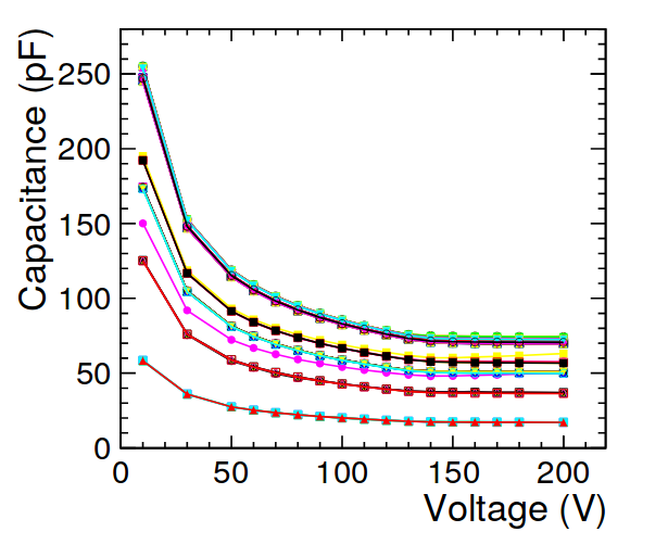
where and are the relative and vacuum permittivity, respectively, and and are the area and the assumed active thickness of the sensor. By plotting as a function of the bias voltage two separate regimes can be observed as a linear rise and a constant behaviour. The full depletion voltage of each sensor can thus be extracted fitting a straight line to each regime or searching for the point of maximum curvature from a quintic spline fit.
3.1 6” Sensor Prototypes
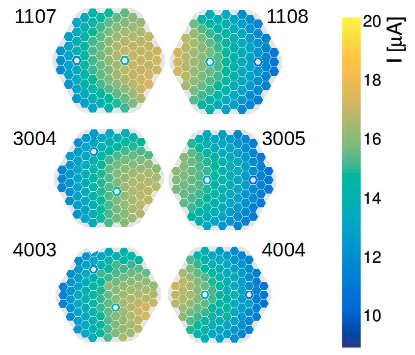
All 6” sensor prototypes tested show a single cell current of about at 1000 V and a total wafer current of at 1000 V. In the atoll p-stop layout it was found that the mask was slightly misaligned which results in a few defective pads for the correspondent prototypes. In figure 4 (left) an example of single cell leakage current for a LD 6” p-type sensor with common p-stop is shown at 1000 V, while in figure 4 (right) the total leakage current in a HD 6” p-type sensor with atoll p-stop is shown as a function of different bias voltages.
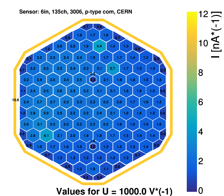
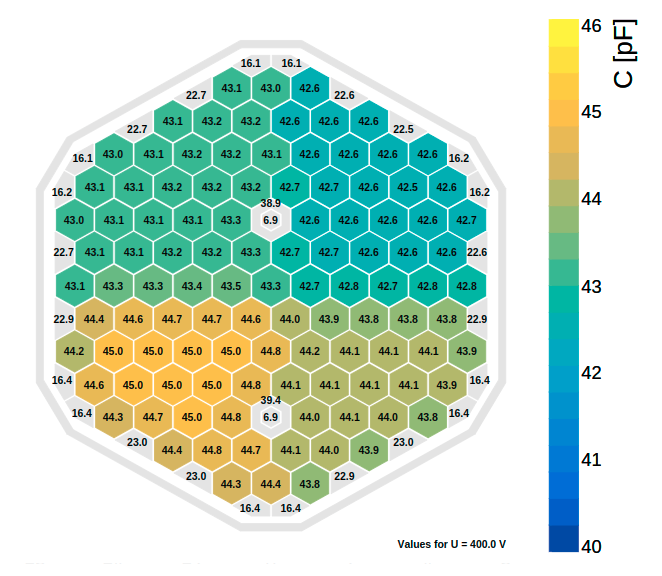
In figure 5 (left) the corrected capacitance for each cell of a LD 6” p-type prototype with atoll p-stop is shown. The four regions with distinct pad-to-pad separations can be clearly seen. The inter-pad capacitance is then plotted in figure 5 (right) as a function of the gap distance for different bulk types and p-stop geometries.
The measured full cell capacitance at full depletion is about for LD 6” prototypes and about for HD 6” prototypes . The depletion voltage was measured between 185 and 300 V and between 50 and 65 V, respectively.
3.1.1 Irradiation Campaign
For validating the radiation hardness of different proposed sensors, eighteen LD 6” prototypes were irradiated in the TRIGA reactor of JSI Ljubljana. The reactor serves as an established reference for neutron irradiations with well-known neutron spectrum and fluence calibration [5].
Three neutron fluences were used in this study: , and . For sensors exposed to the same fluence and excluding the only sensor annealed, similar leakage currents were recorded and a total wafer current of , and at 800 V was measured at , respectively.
In figure 6 (left), the leakage current recorded per single cell is shown for the prototypes irradiated at with different bulk types and p-stop geometries. Further studies are on-going to link the observed gradient in the leakage current across the sensor with the variation of the neutron flux of the reactor beam. In figure 6 (right), the average of the full cell current recorded at a bias voltage of 600 V rescaled for their volume and a temperature of is shown as a function of their respective fluence. The values are also compatible with those obtained in previous studies performed on diodes [2].
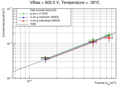
(right) Average of full cell leakage currents as a function of the neutron fluence, measured at and rescaled to , at a bias voltage of 600 V. The measurement is compared to the one obtained in previous studies performed on diodes (dashed black line) [2].
3.2 8” Sensor Prototypes
Assessing the quality of the 8” production process using first sensor prototypes is an important step for the HGCAL project. The wafer technology chosen for the 8” sensor prototypes with 120 active thickness consists of a high-resistivity epitaxial layer on a low resistivity wafer, while for the 200 and 300 ones physically thinned p-type float zone silicon wafers is used.
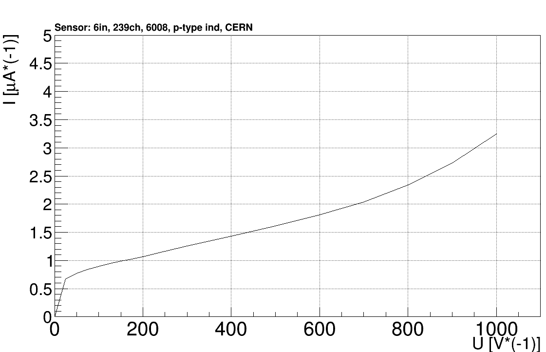
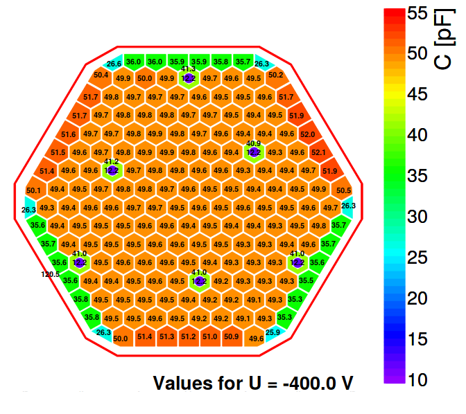
120 prototypes show extremely low leakage currents of at 1000 V, measured full cell capacitance at full depletion of about and depletion voltage between 30 and 40 V. The uniformity of the single cell current is shown in figure 7 (left).
In the case of 200 and 300 prototypes, some cells show high current or breakdown. This issue was found to be related to a back-side fragility in agreement with measurements obtained from HPK and linked to the shallow implant providing the ohmic contact. The measured full cell capacitance at full depletion is about for prototypes with 200 active thickness and about for the 300 ones. The depletion voltage was measured between 120 and 140 V and between 255 and 300 V, respectively. Figure 7 (middle and right) shows an example of the uniformity of the full-size cell capacitance at full depletion and CV curves, respectively, where the different curves correspond to different cell sizes.
The inter-pad capacitance measured for all 8” prototypes tested varies from 3 to depending on the active thickness of the specific sensor under-test. These results are in full agreement with simulation [2] and with measurements performed on 6” prototypes already shown in figure 5.
4 Summary and Next Steps
In 2019 first HPK 8” sensors prototypes were received and electrical characterisation tests were performed to assess the quality of the production process. Irradiation studies are still on-going to better understand the radiation hardness, the oxide quality and oxygen content. Moreover, mitigation actions are currently under study to reduce the issue related to the back-side fragility for 8” prototypes with 200- and 300- active thickness. The full qualification of 8” HPK sensors will continue over the next two years, in view of a mass production starting in the last quarter of 2021.
References
- [1] Apollinari G. et al., High-Luminosity Large Hadron Collider (HL-LHC): Technical Design Report V. 0.1, CERN-2017-007-M (2017) doi:10.23731/CYRM-2017-004.
- [2] CMS Collaboration, The Phase-2 Upgrade of the CMS Endcap Calorimeter, CERN-LHCC-2017-023, CMS-TDR-019 (2019), https://cds.cern.ch/record/2293646.
- [3] CMS Collaboration, P-Type Silicon Strip Sensors for the new CMS Tracker at HL-LHC, JINST 12 (2017) P06018, doi:10.1088/1748-0221/12/06/P06018
- [4] F. Pitters et al., ARRAY: An open source, modular and probe-card based system with integrated switching matrix for characterisation of large area silicon pad sensors, Nucl. Instrum. Methods Phys. Res. A, vol. 940 (2019), pg. 168-173, doi:10.1016/j.nima.2019.06.007.
- [5] V. Radulovic et al., Large Object Irradiation Facility In The Tangential Channel Of The JSI TRIGA Reactor, AIDA-2020-CONF-2017-003 (2017).