Multidimensional Analysis of Excitonic Spectra of Monolayers of Tungsten Disulphide: Towards Computer Aided Identification of Structural and Environmental Perturbations of 2D Materials
Abstract
Despite 2D materials holding great promise for a broad range of applications, the proliferation of devices and their fulfillment of real-life demands are still far from being realized. Experimentally obtainable samples commonly experience a wide range of perturbations (ripples and wrinkles, point and line defects, grain boundaries, strain field, doping, water intercalation, oxidation, edge reconstructions) significantly deviating the properties from idealistic models. These perturbations, in general, can be entangled or occur in groups with each group forming a complex perturbation making the interpretations of observable physical properties and the disentanglement of simultaneously acting effects a highly non-trivial task even for an experienced researcher. Here we generalise statistical correlation analysis of excitonic spectra of monolayer WS2, acquired by hyperspectral absorption and photoluminescence imaging, to a multidimensional case, and examine multidimensional correlations via unsupervised machine learning algorithms. Using principle component analysis we are able to identify 4 dominant components that are correlated with tensile strain, disorder induced by adsorption or intercalation of environmental molecules, multi-layer regions and charge doping, respectively. This approach has the potential to determine the local environment of WS2 monolayers or other 2D materials from simple optical measurements, and paves the way towards advanced, machine-aided, characterisation of monolayer matter.
keywords:
Two-Dimensional Materials, Principle Component Analysis, Hyperspectral ImagingPavel V. Kolesnichenko Qianhui Zhang Changxi Zheng Michael S. Fuhrer Jeffrey A. Davis*
Pavel V. Kolesnichenko
Optical Sciences Centre, Swinburne University of Technology, Melbourne, Victoria 3122, Australia
ARC Centre of Excellence in Future Low-Energy Electronics Technologies, Swinburne University of Technology, Melbourne, Victoria 3122, Australia
Qianhui Zhang
Department of Civil Engineering, Monash University, Victoria 3800, Australia
Changxi Zheng
School of Physics and Astronomy, Monash University, Victoria 3800, Australia
ARC Centre of Excellence in Future Low-Energy Electronics Technologies, Monash University, Victoria 3800, Australia
School of Science, Westlake University, Hangzhou 310024, Zhejiang Province, People’s Republic of China
Institute of Natural Sciences, Westlake Institute for Advanced Study, Hangzhou 310024, Zhejiang Province, People’s Republic of China
Michael S. Fuhrer
School of Physics and Astronomy, Monash University, Victoria 3800, Australia
ARC Centre of Excellence in Future Low-Energy Electronics Technologies, Monash University, Victoria 3800, Australia
Jeffrey A. Davis
Optical Sciences Centre, Swinburne University of Technology, Melbourne, Victoria 3122, Australia
ARC Centre of Excellence in Future Low-Energy Electronics Technologies, Swinburne University of Technology, Melbourne, Victoria 3122, Australia
Email Address:jdavis@swin.edu.au
1 Introduction
Since the realization of exfoliation of a single layer of graphite (graphene) and confirmation of its extraordinary physical properties [1], a wave of efforts aiming at synthesizing other two-dimensional (2D) materials has naturally emerged. A broad spectrum of experimentally obtained ultra-thin materials covering metals [2, 3], semimetals [4], semiconductors [5], insulators [6], topological insulators [7], superconductors [8, 9] and ferromagnets [10] has been already reported with many others having been theoretically predicted [11, 12, 13, 14]. This has opened an avenue to material engineering in the form of van der Waals heterostructures giving rise to novel potential devices such as single-molecule and DNA sensors [15, 16], photodiodes [17, 18], transistors [19], memory cells [20, 21], batteries [22, 23], magnetic field sensors [24], and spintronic logic gates [25, 26].
Despite monolayers holding great promise for a broad range of applications, the research around 2D materials suggests that proliferation of the potential devices and their fulfillment of real-life demands are still far from realization. In contrast to theoretical descriptions of the physical properties of various 2D materials, experimentally obtainable samples commonly experience a wide range of perturbations significantly deviating the properties from idealistic models, and thereby affecting the performance of the devices. Amongst these perturbations are the presence of ripples and wrinkles [27, 28, 29], point and line defects [30, 31], grain boundaries [32], strain fields [33], doping [34, 35, 36, 37]; water intercalation [38]; oxidation [39, 40, 41], and edge reconstructions [42]. These perturbations, in general, can be entangled or occur in groups, forming complex perturbations. This, in turn, makes the interpretations of observable physical properties and the disentanglement of simultaneously acting effects a highly non-trivial task even for an experienced researcher, and advanced characterisation methods are often desirable.
Due to the monolayer nature of 2D materials, their optical signatures are highly sensitive to fluctuations in structure and the local environment. This sensitivity results in non-trivial spatial variations, which are hard to analyse manually, and indicates that unsupervised machine learning algorithms applied to multimodal optical imaging data may aid attempts to identify the fluctuations in structure and the local environment distributed across monolayers.
Here we consider a semiconducting monolayer of tungsten disulphide (WS2) grown via chemical vapour deposition (CVD) on a sapphire substrate. Optical properties of WS2 monolayers are dominated by excitonic effects manifested as intense signatures in their absorption and emission spectra [43]. We apply absorption and photoluminescence (PL) hyperspectral imaging to gather data on the spatial variations of the excitonic properties, which arise from the various perturbations. The spectra are fully parameterised, leading to a multi-dimensional parametric phase-space (hypercube) where a single data point represents the set of values corresponding to all parameters at a given spatial location on the monolayer sample. This then allows us to apply principal component analysis [44, 45, 46] (PCA) to identify the parameters that vary together and ideally combine to quantify specific perturbations and how they vary across the monolayer flake. A projection of the multi-dimensional data-cloud onto a 2D plane with axes given by the two most significant principle components preserves the maximum variance in the data. By using unsupervised K-means clustering [47, 48, 49] of the data-points in this PCA-plane, regions of the sample with similar properties can be identified and provide further insight into how the perturbations combine and vary across the monolayer sample.
2 Results and discussion
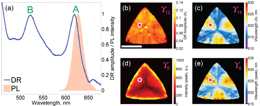
Typical absorption and emission spectra of WS2 monolayers are shown in Figure 1a. Absorption spectra are approximated here by differential reflectance [50, 51, 36] and feature two distinct peaks corresponding to spin-orbit split A- and B-exciton transitions occurring at K symmetry points in the first Brillouin zone [52]. Red-shifted PL emission is evident as an asymmetric peak formed as a result of recombination of excitons and trions [53]. Figure 1b,c shows the spatially-resolved peak absorption amplitude and wavelength corresponding to the A-exciton transition, revealing trigonally-symmetric variations. Similar trends are observed in the spatial maps of PL emission (Figure 1d,e): the absorption and emission are blue-shifted in the regions spanning from the center of the flake towards its apexes. This type of behaviour has been attributed previously to elevated -doping levels in those areas [54, 37], and conversely, red-shifted absorption and emission peaks in the adjacent regions have been shown to result from greater tensile strain [37]. While the absorption and emission wavelength maps are somewhat similar, their difference can reveal variations in Stokes shift, which is closely related to charge doping [36, 37]. More obvious differences are observed between the patterns formed by absorption peak amplitudes (Figure 1b) and emission peak intensities (Figure 1d). The most significant difference is that the edges of the triangular monolayer flake can be clearly distinguished in the PL emission intensity map. Along the edges the PL intensity is enhanced as a result of combined effects of water intercalation progressing towards the interior over time [38] and oxidation [40, 41]. Additionally, three bright spots near the center of the flake can be clearly distinguished in the absorption amplitude map. These bright features are believed to represent multilayer WS2 material formed at the nucleation centers of the monolayer since larger reflectance contrasts have been observed for TMdC multilayers [55]. All these observed differences point to the complementarity of absorption and PL measurements allowing for observations of nonzero correlations between various parameters.
Statistical correlation analysis has been already proven to be a powerful tool in the studies of optoelectronic properties of 2D materials [56, 57, 33, 36, 58, 59, 60]. For example, by correlating spectral shifts of prominent Raman peaks in graphene and graphene/TMdC heterostructures it can be possible to disentangle the effects of doping and strain [56, 59]. Another route to solve a similar problem for TMdC monolayers used correlations involving the PL Stokes shift [37]. Correlation analyses also facilitated the recognition of physically distinct edges of triangular TMdC flakes as domains hosting large number of point defects [57, 60] and the effects of strain on optoelectronic properties of various TMdC monolayers, including direct/indirect nature of the bandgap [33]. All these results, however, were based on scatter plots between specifically chosen pairs of parameters missing out other possible correlations, and were not able to recognise the presence of any subtle variations in the data. Here, we generalise statistical correlation analysis to an -dimensional case to acquire more insights into the optoelectronic variations commonly found in 2D materials.
To make the -dimensional correlation analysis possible we fully parameterise absorption and emission spectra (Figure 2a) and use each of the parameters to represent a dimension of an -dimensional parametric space (Figure 2b), with in our case. This space is represented by an -dimensional hypercube (-cube) encapsulating an -dimensional data-cloud where each data-point is described by a set of values (coordinates), i.e. . The parameters whose spatial variations are mapped in Figure 1b–e correspond to . The definitions of the other parameters and their spatial distributions are given in Supporting Information (Table 1 and Figure 1, respectively). A specific location (pink point in Figure 1b–e) on the monolayer island can, therefore, be assigned a set of numbers corresponding to the values of the 17 parameters chosen to describe the optical properties of the material. We note, that some parameters measure similar quantities (e.g. PL peak intensity and PL integrated intensity), however, there are subtle differences which can be important and so at this stage we include all of them for completeness.
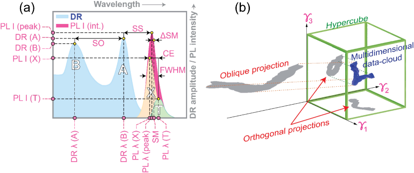
The natural approach to visualization of the geometry of a multi-dimensional object (data-cloud) is to look at its projections onto 2D planes (Figure 2b). Amongst infinite number of possible planes and projecting angles, a particular case of orthogonal projections onto the sides of the -cube is the simplest to realise. It is this particular case that was considered in the previously reported correlation analyses of optoelectronic properties of 2D materials where certain physical trends and clusters have been identified [56, 57, 33, 36, 59, 60, 37]. In some instances, oblique projections can provide greater separation of the data, and in some cases correspond to meaningful parameters. For example, charging energy is defined as the difference between the exciton and trion energy, and would correspond to an oblique projection, as detailed in the Supporting Information.
An example of an orthogonal projection is shown in Figure 3a. In this case, the data is distributed in a ring, which indicates that the full data-cloud is a torus-isomorphic object (other projections showing torus-shaped data-density distributions are shown in Supporting Information). This topology can then also be related to the spatial variations of material properties assuming they vary smoothly, which is typically the case. Specifically, the shape of the data-cloud indicates that it is possible to define loops where each point on the loop has distinct spectral properties (Figure 3b–c). These loops will be around a specific point or points on the material.
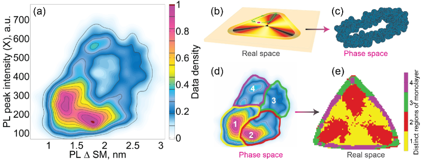
To help visualise this we note that around the data-cloud ring in Figure 3a, there appears to be four main clusters of data, as identified in Figure 3d. The boundaries are defined as the lines connecting those points of the data density contours that have high negative curvature [61, 62] (see Supporting Information for estimation of curvatures). The data-points within each cluster are mapped back into their real-space location in Figure 3e, showing that the clusters are indeed related to specific regions on the sample. The points about which the circular paths can be identified, are the points where the four colours (corresponding to the four clusters) meet. It is apparent then that by selecting specific orthogonal projections and subsequent clustering analysis, we can gain some insight into how the optical properties (and corresponding structural/environment properties) vary across the sample. However, it is likely that there is further fine structure in these clusters, indeed, it is expected that many of the sample perturbations vary smoothly and continuously. These perturbations will affect the 17 different parameters in different ways, and in most cases will affect more than one parameter. To identify the parameters that vary together and maintain the maximum variance of the data, we apply the principal component analysis (PCA) [44, 45, 46]. By identifying the orthogonal principle components (i.e. specific linear combinations of the 17 parameters) that maintain the maximal variance, the ability to resolve fine structure and small variations in the data cloud is enhanced. Furthermore, in identifying the parameters that vary together, this approach has the potential to separate each specific sample perturbation (e.g. strain, doping, molecular adsorption, etc.) and the specific changes to the optical properties induced by each of them. It may then become possible to map the structural and environmental properties across the sample.
The method for PCA has been described previously [44, 45, 46] and the details of the approach used here are included in the Supporting Information. The result is a new set of axes (the principle components) for the data hypercube. These principle components are defined such that the variances of the data along the principal components (PC) decrease for each successive component (i.e. ) with corresponding to the maximal variance of the data (distributed along PC1). The corollary of defining the principle components in this way is that it also identifies the measurement parameters that vary together, and distills the variance of the 17-dimensional data-cloud into a hypercube of a lower dimensionality. In the case of the hypercube defined by the parameters of absorption and emission spectra considered here, the PCA approach showed that it is possible to reduce the number of dimensions from 17 (defined by the parameters ) down to 4 (defined by the parameters PC1, …,PC4) and still preserve as much as 87.9% of the total variance (see Supporting Information).
Each of the principle components are formed by a linear combination of the measurement parameters. The relative weight of the parameters for each PC is shown in the Supporting information, Table 2. The amplitude of each principle component then varies across the sample and can be mapped spatially in the same way the measurement parameters were mapped in Figure 1b–e. Based on the make-up of each PC, their spatial variations across the WS2 flake, and previously reported understanding of these materials, we are able to correlate each PC with a specific perturbation (or group of perturbations) of the sample structure and/or environment. Specifically, we link PC1 with variations in strain, PC2 with disorder induced by adsorption and/or intercalation of environmental molecules, PC3 with multilayers and PC4 with charge doping.
The attribution of PC1 to strain variation is based on the observation that the dominant contributions to this component are the PL intensity and wavelength parameters, as well as the absorption wavelength for the A-exciton, consistent with previous measurements reporting the effect of strain on optical properties [63, 55, 64]. In addition, the spatial variation of PC1 across the sample (Figure 4a) is consistent with previous observations of how the strain varies from the apexes to the middle of the sides in CVD-grown WS2 monolayers [65, 66, 37]. There are other perturbations that can also alter the PL intensities and wavelengths, however, these also affect other parameters that are absent from this principle component (e.g. doping also leads to substantial Stokes shift). PC2 (Figure 4b) is dominated by variations in the PL FWHM, SM, and charging energy (CE). Alone, SM and CE can be associated with doping density, however, a clearer signature of doping is the Stokes shift [54, 36, 37], which doesn’t make a significant contribution to this PC. Furthermore, this is a flake that has been exposed to air for some time and previous work has shown that where freshly grown flakes have large amounts of -doping in the region of the apexes, the aged flakes adsorb environmental molecules, which reduce the density of free charges, and increase the FWHM [67, 36, 68, 37]. The spatial variation of PC2 adds further weight to this assignment, as in addition to the expected variations in the bulk of the 2D flake, it also reveals the edges where water intercalation has occurred [38, 37].

PC3 is dominated by the DR peak intensity for both A- and B-excitons, and the spatial map shows the most significant variance occurs in small regions near the centre of the flake. This is consistent with previous measurements that have attributed significant increases in DR intensity to increased scattering from multi-layer regions on the sample [69, 70]. The dominant contribution to PC4 is the PL Stokes shift, which is strongly linked with charge doping [54, 36, 37]. The relatively low level of data variation in PC4-map is consistent with previous observations of small variations of doping density on aged CVD-grown flakes. Interestingly, the other significant contribution to PC4 is the effective spin-orbit splitting, or in other words the energy difference between the A- and B-excitons in the DR measurements. It was previously speculated that these variations could be due to increased doping [37], but other possibilities couldn’t be ruled out. This observation adds further weight to the case that it is due to variations in doping density.
The ability to self-consistently attribute specific sample perturbations to the four primary principle components that arise naturally from PCA of a single flake is potentially of great value. It points to the possibility of developing a set of well-defined principle components, consisting of linear combinations of spectroscopic parameters, that could be applied to determine the precise structural and environmental perturbations at a specific location in a 2D semiconductor. Further analysis of how these perturbations vary across the flakes could then provide insight into growth mechanisms and causes of the variations from pristine materials. We note, however, that to have a greater level of confidence in the make-up of the significant principle components and their relationship to physical perturbations, analysis of a larger dataset and materials prepared under different conditions with different combinations of perturbations is required. This will be the subject of future work.
One of the challenges that may be resolved by this type of PCA is the ability to distinguish different contributions, where multiple perturbations occur at the same place. To demonstrate this we project the data onto the plane spanned by the first two principal components (PC1 and PC2) (Figure 4c), associated with strain and the adsorption of environmental molecules and/or intercalation of water. This projection shows the maximum spread of the data and reveals some clustering of data points. In order to acquire more insights into the projected data and correlate the coordinates in this PC1-PC2 plane with the spatial location on the WS2 flake, we applied the K-means-clustering unsupervised learning algorithm [47, 48, 49]. This algorithm, for a given input number , tries to classify the data-set into labeled clusters (see Supporting Information for details). The value of , however, cannot be automatically identified by the algorithm, and, therefore, cluster identification methods are commonly used. Here we used the so called “elbow” method [71] as one of the most popular methods for identification of the natural number of clusters, if there are any (see Supporting Information). As expected, in the case of the WS2 monolayer considered here, the “elbow” method revealed the presence of four prominent clusters in the data-cloud (see Supporting Information) corresponding to the two heterogeneous interior domains and two heterogeneous edge domains within the flake, as identified above in Figure 3. However, the method also revealed that there are other natural cluster sets (, and ) present in the data, although they are not as prominent as the set of 4 clusters (). With increasing the number of clusters , additional “shades” are introduced to the cluster set (Figure 4c). We note that we excluded multilayer regions, which are separated from the rest of the data cloud in the PC3 component (gray data-points in Figure 4c), from the K-means analysis by treating them as “anomalies” (or “outliers”) [72].
We then mapped the data-points in the PCA-plane within each of the clusters back onto the monolayer flake (Figure 4d) revealing fine-structure of the four main regions of the sample mentioned above. These four clusters can be clearly grouped in pairs, with the purple and green regions mapping the edges affected by water intercalation, and the red and yellow regions mapping the interior of the flake. This roughly correlates with the higher values for PC2 around the edges, although it can also be seen that the value of PC2 increases when going from purple to green. A similar trend is seen when going from yellow to red in the interior. This indicates that while the main change in going from yellow to red and purple to green is along the PC1 axis, and due to reducing tensile strain, this trend is accompanied by an increase in disorder due to adsorbed molecules, and hence a shift along the PC2 axis.
We note also that water intercalation does not change appreciably the amount of strain along the edges, as evidenced by the consistent variation along PC1 for both the edges and interior. This suggests that on average the strain field vectors are aligned angularly around the center of the monolayer island so that the radially-propagating water intercalation does not release strain (see also Supporting Information, Section 10).
3 Conclusions
These results indicate that the principle component analysis based on the spectral parameters from PL and DR hyperspectral imaging, has the potential to disentangle and quantify different types of perturbations in monolayer materials. This approach is effectively an extension of specific 2D correlation plots that have been used to help understand the variations across a monolayer flake [56, 57, 33, 36, 59, 60, 37], and which were used here to reveal different regions of the monolayer flake with clearly different combinations of perturbations. The principle component analysis, however, is a more systematic and quantitative approach.
The PCA applied to the data here produced four dominant, orthogonal principle components. By examining the combination of spectral parameters that makes up each of these, and the variation of these PCs across the flake, we were able to assign a specific sample perturbation to each: tensile strain, disorder induced by adsorption/intercalation of environmental molecules, multi-layers, and charge doping. These assignments, the spatial variations and spectral parameters contributing are fully consistent with previous measurements and understanding developed from similar flakes [69, 70, 63, 65, 66, 55, 64, 37]. However, these assignments are not definitive and may not be able to reliably predict the specific perturbations on a different flake. It does, however, point to the possibility of using this approach for this purpose. To achieve this, a larger sample size including multiple flakes with different levels of the different perturbations is needed, and a refinement of the parameters may be necessary to remove the intensity/amplitude parameters, which depend on the measurement system. Subsequent steps could involve a large labeled dataset, and combinations of PCA and cluster analysis to train neural networks and enable real-time identification of spatially-varying perturbation. Regardless, the demonstration here that a self-consistent attribution can be made using PCA on a single flake indicates that this approach is promising, and may allow creation of a tool capable of identifying the perturbations at a given location in a given 2D material simply from PL and DR spectra.
4 Experimental Section
4.1 Sample preparation
The sample preparation was performed in a similar way as described in Ref. [73]. Briefly, monolayers of WS2 were grown on sapphire substrate via CVD using WO3 and sulphur precursors. WO3 precursor was placed in the middle of the chamber (high-temperature zone, 860C) while the sulphur precursor was placed further upstream (low-temperature zone, 180C). The substrate was placed in a direct proximity to the WO3 precursor. Heating the chamber and maintaining the hot environment lasted over 45 min, after which a cooling process was initiated.
4.2 Experimental realization
The PL and DR imaging setups were implemented in the same way as described in Ref. [37]. In a nutshell, in PL experiments, linearly polarised cw radiation (410 nm) was focused on the sample through a 100x objective lens (NA=0.95). The detection scheme was implemented in an epi-fluorescence geometry in a confocal way with the detection spatial resolution reaching 300 nm. DR measurements were performed using a broadband (400–800 nm) incoherent white light radiation with the detection spatial resolution reaching 380 nm.
Supporting Information
Supporting Information is available from the Wiley Online Library.
Acknowledgements
This work was supported by the Australian Research Council Centre of Excellence for Future Low-Energy Electronics Technologies (CE170100039).
References
- [1] K. S. Novoselov, Science 2004, 306, 5696 666.
- [2] A. Courty, A.-I. Henry, N. Goubet, M.-P. Pileni, Nature Materials 2007, 6, 11 900.
- [3] Y. Ma, B. Li, S. Yang, Materials Chemistry Frontiers 2018, 2, 3 456.
- [4] J. Kim, S. S. Baik, S. H. Ryu, Y. Sohn, S. Park, B.-G. Park, J. Denlinger, Y. Yi, H. J. Choi, K. S. Kim, Science 2015, 349, 6249 723.
- [5] A. Splendiani, L. Sun, Y. Zhang, T. Li, J. Kim, C.-Y. Chim, G. Galli, F. Wang, Nano Letters 2010, 10, 4 1271.
- [6] K. Zhang, Y. Feng, F. Wang, Z. Yang, J. Wang, Journal of Materials Chemistry C 2017, 5, 46 11992.
- [7] L. Kou, Y. Ma, Z. Sun, T. Heine, C. Chen, The Journal of Physical Chemistry Letters 2017, 8, 8 1905.
- [8] G. C. Ménard, S. Guissart, C. Brun, R. T. Leriche, M. Trif, F. Debontridder, D. Demaille, D. Roditchev, P. Simon, T. Cren, Nature Communications 2017, 8, 1 2040.
- [9] G. C. Ménard, A. Mesaros, C. Brun, F. Debontridder, D. Roditchev, P. Simon, T. Cren, Nature Communications 2019, 10, 1 2587.
- [10] B. Huang, G. Clark, E. Navarro-Moratalla, D. R. Klein, R. Cheng, K. L. Seyler, D. Zhong, E. Schmidgall, M. A. McGuire, D. H. Cobden, W. Yao, D. Xiao, P. Jarillo-Herrero, X. Xu, Nature 2017, 546, 7657 270.
- [11] J. C. Garcia, D. B. de Lima, L. V. C. Assali, J. F. Justo, The Journal of Physical Chemistry C 2011, 115, 27 13242.
- [12] A. N. Andriotis, E. Richter, M. Menon, Physical Review B 2016, 93, 8 081413(R).
- [13] W. Ding, J. Zhu, Z. Wang, Y. Gao, D. Xiao, Y. Gu, Z. Zhang, W. Zhu, Nature Communications 2017, 8, 1 14956.
- [14] T. Olsen, E. Andersen, T. Okugawa, D. Torelli, T. Deilmann, K. S. Thygesen, Physical Review Materials 2019, 3, 2 024005.
- [15] H. Arjmandi-Tash, L. A. Belyaeva, G. F. Schneider, Chemical Society Reviews 2016, 45, 3 476.
- [16] H. Qiu, A. Sarathy, K. Schulten, J.-P. Leburton, npj 2D Materials and Applications 2017, 1, 1 3.
- [17] M. M. Furchi, A. Pospischil, F. Libisch, J. Burgdörfer, T. Mueller, Nano Letters 2014, 14, 8 4785.
- [18] C.-H. Lee, G.-H. Lee, A. M. van der Zande, W. Chen, Y. Li, M. Han, X. Cui, G. Arefe, C. Nuckolls, T. F. Heinz, J. Guo, J. Hone, P. Kim, Nature Nanotechnology 2014, 9, 9 676.
- [19] T. Georgiou, R. Jalil, B. D. Belle, L. Britnell, R. V. Gorbachev, S. V. Morozov, Y.-J. Kim, A. Gholinia, S. J. Haigh, O. Makarovsky, L. Eaves, L. A. Ponomarenko, A. K. Geim, K. S. Novoselov, A. Mishchenko, Nature Nanotechnology 2012, 8, 2 100.
- [20] S. Bertolazzi, D. Krasnozhon, A. Kis, ACS Nano 2013, 7, 4 3246.
- [21] M. S. Choi, G.-H. Lee, Y.-J. Yu, D.-Y. Lee, S. H. Lee, P. Kim, J. Hone, W. J. Yoo, Nature Communications 2013, 4, 1.
- [22] E. Pomerantseva, Y. Gogotsi, Nature Energy 2017, 2, 7 17089.
- [23] P. Zhang, F. Wang, M. Yu, X. Zhuang, X. Feng, Chemical Society Reviews 2018, 47, 19 7426.
- [24] V. O. Jimenez, V. Kalappattil, T. Eggers, M. Bonilla, S. Kolekar, P. T. Huy, M. Batzill, M.-H. Phan, arXiv 2019, 1902.08365, 1902.08365.
- [25] R. K. Kawakami, 2D Materials 2015, 2, 3 034001.
- [26] W. Han, APL Materials 2016, 4, 3 032401.
- [27] J. Brivio, D. T. L. Alexander, A. Kis, Nano Letters 2011, 11, 12 5148.
- [28] L. Tapasztó, T. Dumitrică, S. J. Kim, P. Nemes-Incze, C. Hwang, L. P. Biró, Nature Physics 2012, 8, 10 739.
- [29] W. Zhu, T. Low, V. Perebeinos, A. A. Bol, Y. Zhu, H. Yan, J. Tersoff, P. Avouris, Nano Letters 2012, 12, 7 3431.
- [30] J. C. Meyer, C. Kisielowski, R. Erni, M. D. Rossell, M. F. Crommie, A. Zettl, Nano Letters 2008, 8, 11 3582.
- [31] H.-P. Komsa, S. Kurasch, O. Lehtinen, U. Kaiser, A. V. Krasheninnikov, Physical Review B 2013, 88, 3 035301.
- [32] A. M. van der Zande, P. Y. Huang, D. A. Chenet, T. C. Berkelbach, Y. You, G.-H. Lee, T. F. Heinz, D. R. Reichman, D. A. Muller, J. C. Hone, Nature Materials 2013, 12, 6 554.
- [33] W.-T. Hsu, L.-S. Lu, D. Wang, J.-K. Huang, M.-Y. Li, T.-R. Chang, Y.-C. Chou, Z.-Y. Juang, H.-T. Jeng, L.-J. Li, W.-H. Chang, Nature Communications 2017, 8, 1 929.
- [34] B. Liu, W. Zhao, Z. Ding, I. Verzhbitskiy, L. Li, J. Lu, J. Chen, G. Eda, K. P. Loh, Advanced Materials 2016, 28, 30 6457.
- [35] Y. Kang, S. Han, Nanoscale 2017, 9, 12 4265.
- [36] N. J. Borys, E. S. Barnard, S. Gao, K. Yao, W. Bao, A. Buyanin, Y. Zhang, S. Tongay, C. Ko, J. Suh, A. Weber-Bargioni, J. Wu, L. Yang, P. J. Schuck, ACS Nano 2017, 11, 2 2115.
- [37] P. V. Kolesnichenko, Q. Zhang, T. Yun, C. Zheng, M. S. Fuhrer, J. A. Davis, 2D Materials 2019.
- [38] C. Zheng, Z.-Q. Xu, Q. Zhang, M. T. Edmonds, K. Watanabe, T. Taniguchi, Q. Bao, M. S. Fuhrer, Nano Letters 2015, 15, 5 3096.
- [39] Y. Zhang, Y. Zhang, Q. Ji, J. Ju, H. Yuan, J. Shi, T. Gao, D. Ma, M. Liu, Y. Chen, X. Song, H. Y. Hwang, Y. Cui, Z. Liu, ACS Nano 2013, 7, 10 8963.
- [40] Z. Hu, J. Avila, X. Wang, J. F. Leong, Q. Zhang, Y. Liu, M. C. Asensio, J. Lu, A. Carvalho, C. H. Sow, A. H. C. Neto, Nano Letters 2019, 19, 7 4641.
- [41] J. C. Kotsakidis, Q. Zhang, A. L. V. de Parga, M. Currie, K. Helmerson, D. K. Gaskill, M. S. Fuhrer, Nano Letters 2019, 19, 8 5205.
- [42] W. Zhou, X. Zou, S. Najmaei, Z. Liu, Y. Shi, J. Kong, J. Lou, P. M. Ajayan, B. I. Yakobson, J.-C. Idrobo, Nano Letters 2013, 13, 6 2615.
- [43] H. R. Gutiérrez, N. Perea-López, A. L. Elías, A. Berkdemir, B. Wang, R. Lv, F. López-Urías, V. H. Crespi, H. Terrones, M. Terrones, Nano Letters 2012, 13, 8 3447.
- [44] K. Pearson, The London, Edinburgh, and Dublin Philosophical Magazine and Journal of Science 1901, 2, 11 559.
- [45] H. Hotelling, Journal of Educational Psychology 1933, 24, 6 417.
- [46] J. Lever, M. Krzywinski, N. Altman, Nature Methods 2017, 14, 7 641.
- [47] S. Hugo, Bull. Acad. Pol. Sci., Cl. III 1957, 4 801.
- [48] J. MacQueen, In Proceedings of the Fifth Berkeley Symposium on Mathematical Statistics and Probability, Volume 1: Statistics. University of California Press, Berkeley, Calif., 1967 281–297, URL https://projecteuclid.org/euclid.bsmsp/1200512992.
- [49] S. Lloyd, IEEE Transactions on Information Theory 1982, 28, 2 129.
- [50] J. McIntyre, D. Aspnes, Surface Science 1971, 24, 2 417.
- [51] A. Chernikov, C. Ruppert, H. M. Hill, A. F. Rigosi, T. F. Heinz, Nature Photonics 2015, 9, 7 466.
- [52] G.-B. Liu, D. Xiao, Y. Yao, X. Xu, W. Yao, Chemical Society Reviews 2015, 44, 9 2643.
- [53] J. W. Christopher, B. B. Goldberg, A. K. Swan, Scientific Reports 2017, 7, 1.
- [54] K. F. Mak, K. He, C. Lee, G. H. Lee, J. Hone, T. F. Heinz, J. Shan, Nature Materials 2012, 12, 3 207.
- [55] R. Frisenda, Y. Niu, P. Gant, A. J. Molina-Mendoza, R. Schmidt, R. Bratschitsch, J. Liu, L. Fu, D. Dumcenco, A. Kis, D. P. D. Lara, A. Castellanos-Gomez, Journal of Physics D: Applied Physics 2017, 50, 7 074002.
- [56] J. E. Lee, G. Ahn, J. Shim, Y. S. Lee, S. Ryu, Nature Communications 2012, 3, 1 1024.
- [57] W. Bao, N. J. Borys, C. Ko, J. Suh, W. Fan, A. Thron, Y. Zhang, A. Buyanin, J. Zhang, S. Cabrini, P. D. Ashby, A. Weber-Bargioni, S. Tongay, S. Aloni, D. F. Ogletree, J. Wu, M. B. Salmeron, P. J. Schuck, Nature Communications 2015, 6, 1 7993.
- [58] L. Wang, C. Xu, M.-Y. Li, L.-J. Li, Z.-H. Loh, Nano Letters 2018, 18, 8 5172.
- [59] R. Rao, A. E. Islam, S. Singh, R. Berry, R. K. Kawakami, B. Maruyama, J. Katoch, Physical Review B 2019, 99, 19 195401.
- [60] C. Kastl, R. J. Koch, C. T. Chen, J. Eichhorn, S. Ulstrup, A. Bostwick, C. Jozwiak, T. R. Kuykendall, N. J. Borys, F. M. Toma, S. Aloni, A. Weber-Bargioni, E. Rotenberg, A. M. Schwartzberg, ACS Nano 2019, 13, 2 1284.
- [61] M. Morisawa, Transactions, American Geophysical Union 1957, 38, 1 86.
- [62] J. D. Pelletier, Water Resources Research 2013, 49, 1 75.
- [63] Q. Zhang, Z. Chang, G. Xu, Z. Wang, Y. Zhang, Z.-Q. Xu, S. Chen, Q. Bao, J. Z. Liu, Y.-W. Mai, W. Duan, M. S. Fuhrer, C. Zheng, Advanced Functional Materials 2016, 26, 47 8707.
- [64] I. Niehues, R. Schmidt, M. Drüppel, P. Marauhn, D. Christiansen, M. Selig, G. Berghäuser, D. Wigger, R. Schneider, L. Braasch, R. Koch, A. Castellanos-Gomez, T. Kuhn, A. Knorr, E. Malic, M. Rohlfing, S. M. de Vasconcellos, R. Bratschitsch, Nano Letters 2018, 18, 3 1751.
- [65] K. M. McCreary, A. T. Hanbicki, S. Singh, R. K. Kawakami, G. G. Jernigan, M. Ishigami, A. Ng, T. H. Brintlinger, R. M. Stroud, B. T. Jonker, Scientific Reports 2016, 6, 1 35154.
- [66] K. M. McCreary, M. Currie, A. T. Hanbicki, H.-J. Chuang, B. T. Jonker, ACS Nano 2017, 11, 8 7988.
- [67] M. S. Kim, S. J. Yun, Y. Lee, C. Seo, G. H. Han, K. K. Kim, Y. H. Lee, J. Kim, ACS Nano 2016, 10, 2 2399.
- [68] L. Sun, X. Zhang, F. Liu, Y. Shen, X. Fan, S. Zheng, J. T. L. Thong, Z. Liu, S. A. Yang, H. Y. Yang, Scientific Reports 2017, 7, 1.
- [69] K. P. Dhakal, D. L. Duong, J. Lee, H. Nam, M. Kim, M. Kan, Y. H. Lee, J. Kim, Nanoscale 2014, 6, 21 13028.
- [70] A. Castellanos-Gomez, J. Quereda, H. P. van der Meulen, N. Agraït, G. Rubio-Bollinger, Nanotechnology 2016, 27, 11 115705.
- [71] M. S. Aldenderfer, R. K. Blashfield, Cluster Analysis (Quantitative Applications in the Social Sciences), SAGE Publications, Inc, 1984.
- [72] V. Chandola, A. Banerjee, V. Kumar, ACM Computing Surveys 2009, 41, 3 1.
- [73] Q. Zhang, J. Lu, Z. Wang, Z. Dai, Y. Zhang, F. Huang, Q. Bao, W. Duan, M. S. Fuhrer, C. Zheng, Advanced Optical Materials 2018, 6, 12 1701347.
See pages - of suppl_PK.pdf