Memory effect in the charge transport in strongly disordered antimony films
Abstract
We study conductivity of strongly disordered amorphous antimony films under high bias voltages. We observe non-linear current-voltage characteristic, where the conductivity value at zero bias is one of two distinct values, being determined by the sign of previously applied voltage. Relaxation curves demonstrate high stability of these conductivity values on a large timescale. Investigations of the antimony film structure allows to determine the percolation character of electron transport in strongly disordered films. We connect the memory effect in conductivity with modification of the percolation pattern due to recharging of some film regions at high bias voltages.
pacs:
71.30.+h, 72.15.Rn, 73.43.NqI Introduction
Recently, considerable interest is attracted by structures with a memory effect, where the electrical resistance depends on the measurement backstory mem1 ; mem2 . In many cases, e.g. for MOSFETs, the resistance of the dielectric layer can be irreversibly affected by high gate voltages, so this new dielectric state maintains after removing the gate voltage. On the other hand, structures are possible in which the resistance at zero bias is controlled by the sign/value of the previously transmitted current. For the first time such structures were considered theoretically chua as the fourth missing element of electrical circuits, and were called as a "memristor". Although there are some doubts about practical implementation of the memristor model ventra , this topic is attracting significant interest not only due to the practical potential for signal processing, storing information inf , but also due to the general interest to physical processes which lead to reversible resistance change in various structures.
There are two main approaches to the practical realization of resistance memory effects: (i) three-layer vertical metal-dielectric-metal structures, where the resistance is determined by ion diffusion within the dielectric layer (see, e.g., Refs tulina, ; vedeneev, and references herein); (ii) systems with phase transition, which occurs between crystalline and amorphous states under the control current pulse (see, e.g., Ref. phase, as a review). Well known drawbacks of these systems are the relatively slow performance rate, and also the low lifetime (about 100 cycles) in the first case because of the poorly controlled ion diffusion process.
On the over hand, there are many important results in the field of electron transport of strongly disordered systems near the metal-dielectric transition dolgop ; gantm . The effects observed, e.g., evolution of the current percolation pattern shklovskii under the influence of external factors, can be the basis for novel realizations of resistive memory effects. In this case, the restrictions are reduced on the low switching rate and sample survival in successive cycles due to electron transport instead of the ion one. This topic is also of general physical interest, since observation and investigation the resistive memory effects can provide addition information on charge transport in strongly disordered systems.
Here, we study conductivity of strongly disordered amorphous antimony films under high bias voltages. We observe non-linear current-voltage characteristic, where the conductivity value at zero bias is one of two distinct values, being determined by the sign of previously applied voltage. Relaxation curves demonstrate high stability of these conductivity values on a large timescale. Investigations of the antimony film structure allows to determine the percolation character of electron transport in strongly disordered films. We connect the memory effect in conductivity with modification of the percolation pattern due to recharging of some film regions at high bias voltages.
II Samples and techniques
As for electron structure, antimony is a standard semimetal with relatively low carrier concentration. It has several allotropic modifications in crystal and amorphous states, the conductivity of amorphous and crystal antimony differs by four orders of magnitude maki . One of the amorphous modification is the black antimony, which can be produced by thermal evaporation on the amorphous substrate. The obtained film is amorphous for thicknesses below 10 nm, it has two-phase amorphous-crystalline structure for film thicknesses up to 120 nm, and it is a crystal for higher thicknesses. The exact critical thickness values depend on the deposition speed and the substrate temperature hashimoto .
Our samples are the thin antimony films with 20 nm thickness. The film thickness and the evaporation parameters are chosen to have strongly disordered state of the film in terms of both short- and long-range potential fluctuations. Antimony is deposited trough the cracking zone (820∘ C) on a glass (amorphous) substrate. The evaporation rate is 0.5 Å/sec at the crucible temperature 440∘ C. After deposition, the amorphous film structure is confirmed by x-ray diffraction method. As a reference sample, we use similarly evaporated film on a standard silicon wafer.
For transport measurements, we fabricate Ohmic contacts by conventional ultrasonic bonding of aluminum wires. This results in aluminium contacts of about 20 m size. The bonding provides reliable destruction of any oxide/contamination layers between the film and the wire materials, which results in good Ohmic contact. For amorphous films, cold bonding process has advantages over the standard lithographic methods, since there is no risk of sample crystallization fisher due to essential sample heating at the resist baking (90-130∘ C) and contacts evaporation steps.
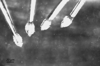
The contacts are placed in the central part of a lengthy film (approximately mm2) at the distances of 20-30 m between the contacts, see Fig. 1. This geometry allows to avoid any edge effects in distributions of electric fields and current flow paths. In addition, it allows to study the structure of the film between the contacts by atomic force and scanning electron microscopy techniques.
To apply high bias voltages to the sample (up to 10 V), the measurements are performed in a two-point technique: the bias voltage is applied between the contacts, while the current is measured in the circuit. One of the contacts in Fig. 1 is grounded, the applied voltage varies within 10 V range at the neighbor contact, which corresponds to the maximum current of about 0.1 mA through the sample. To obtain differential conductivity curves , the applied voltage is additionally modulated by a small (4.4 mV) ac component at a frequency of 1100 Hz. The ac current component is measured by lock-in, being proportional to differential conductivity at a given bias voltage . We verify that the obtained value does not depend on the modulation frequency in the range 100 Hz–1 kHz, which is determined by the applied filters. Due to the high quality of Ohmic contacts, their resistances are much below the resistance of a disordered antimony film (more than 100 kOhm). Also, the contact quality is confirmed by measurements of a reference sample (which is the antimony film on a silicon surface), which demonstrates the resistance values less than 100 Ohm in a two-point technique. All the measurements are carried out at room temperature in zero magnetic field.
III Experimental results
Fig. 2 shows examples of experimental curves, which demonstrate dependences of differential conductivity on the applied bias voltage for two different samples, in (a) and (b), respectively. In both the cases, the 20 m-long regions of antimony films show large resistance at zero bias voltage (more than 100 kOhm) and strongly non-Ohmic behavior of . Namely, differential conductivity increases in about 2 times in a sweep of from zero to 10 V. Every curve shows a kink in the middle of the range, at higher biases the differential conductivity is a linear function of . The nonlinear behavior of differential resistance is also observed for the reference sample of an antimony film on a polished oxidized silicon surface, see the inset to Fig. 2 (a). However, the measured value of differential resistance is significantly smaller (over three orders of magnitude) for the reference sample for similar sample geometry. This resistance difference of two antimony films corresponds to the expected values for amorphous (on the glass substrate) and crystalline (on the silicon one) films maki : from the sample dimensions, the antimony resistivity can be estimated as 0.5 Ohmcm and Ohmcm, respectively.
To our surprise, there is a hysteresis in the experimental curves for two different sweep directions, see Fig. 2. Namely, if the linear parts of curves are within the sweep range, the sample differential conductivity at zero bias depends on the sweep direction. Qualitatively, this effect is well reproducible for different samples, cp. panels (a) and (b) in Fig. 2, while both the amplitude and the sign of the effect vary from sample to sample. For a given sample, curves are well reproducible in at least 100 voltage scans. In addition, depends on the sweep rate: when it is decreased by an order of magnitude, the curves coincide at high voltages , while the nonzero difference can still be clearly seen even for the lowest sweep rate, see the inset to Fig. 2 (b). We don’t observe any hysteresis effects for the reference films on a silicon substrate.
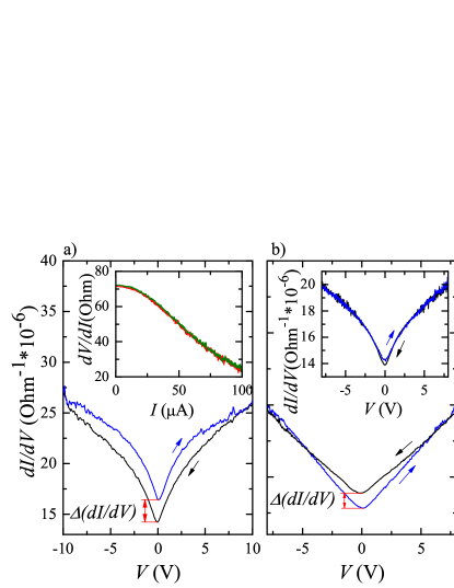
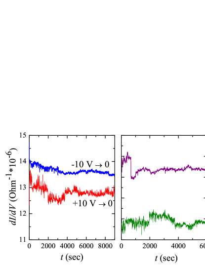
The observed dependence of a hysteresis amplitude on the sweep rate means that there are some relaxation processes in electron transport in strongly disordered antimony films. For this reason, we directly investigate relaxation for our samples, see Fig. 3 (a). To realize a procedure, we keep the sample for about 10 minutes at high bias 10 V, which is obviously higher than the kink voltage value of curves. After that we reset the bias to zero and immediately start tracing the difference conductivity in dependence of time. The obtained relaxation curves show small (below 10%) relaxation for the first 3000 seconds, the value is stable afterward, see Fig. 3 (a). This stable value obviously depends on a sign of initial bias voltage. It well corresponds to the sign and the amplitude of the hysteresis for this sample in Fig. 2 (b). Fig. 3 (b) directly demonstrates the hysteresis amplitude for two samples from Fig. 2 (a) and (b), where is obtained by subtracting two relaxation curves for each sample.
IV Discussion
As a result, we demonstrate a memory effect for differential conductivity of a sample at zero bias voltage : there are two distinct conductance values, switching between them is obtained by applying significant bias of a different sign. In addition, we show that these sample states remain stable on macroscopic time scales (several hours). It indicates that significant bias voltage applied between 20 m spaced contacts leads to a stable change of the current distribution pattern in strongly disordered antimony films. This process is well reproducible for different samples and in multiple cycles, i.e. sample switching is well reversible procedure.
To explain the observed memory effect it should be noted, that in case of thin amorphous antimony film there are no reversible phase transitions between amorphous and crystalline states fisher . In other words, an amorphous antimony film can be transformed into a crystalline state of -antimony by heating, but the backward transition from a crystalline state into an amorphous one can not be made by melt quenching. Moreover, we observe a well developed memory effect at low sweep rates. Therefore, phase transitions can not be considered in antimony films as a mechanism of the observed memory effect phase . Also, for the lateral sample geometry, the diffusion of dopant ions from electrodes can not be considered for 20 m-long monocomponent film, in contrast to thin three-layer planar structures metal-insulator-metal tulina . In the latter case, for a comparable potential difference at the electrodes 10 V, it drops on a 100 nm thick dielectric layer, which corresponds vedeneev to the V/cm electric field. In our case, the ion diffusion might only be possible from aluminum contacts in their vicinity. Due to the high resistance of the film and low contact resistance (see the main figure and the insert to Fig. 2 (a)), the contact areas are of negligible contribution to the resistance of 20 m-long sample. Moreover the average electric field V/cm is too small for the diffusion process.
On the over hand, the zero-bias sample resistance corresponds to resistivity 0.5 Ohmcm, so the film is in a dielectric state according to Ioffe-Regel criterion gantm . Such strongly disordered thin films usually demonstrates percolation current patterns shklovskii , which could be affected by significant bias voltage. Fig. 4 shows the electron microscope image of the investigated antimony film on a glass substrate. This film is of granular structure and shows coagulation of deposited particles, which is a fingerprint of amorphous antimony films obtained by low-rate deposition palatnik . Coagulated conglomerates of deposited particles can be seen as light gray contrast areas with lengths from 300 nm to 1 m. Fig. 4 well corresponds to a typical pattern of percolation clusters for strongly disordered materials shklovskii . For a reference film on a polished silicon wafer, crystalline phase dominates, which leads to low resistivity values without noticeable memory effects butenko .
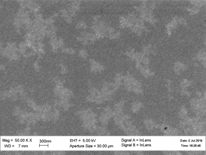
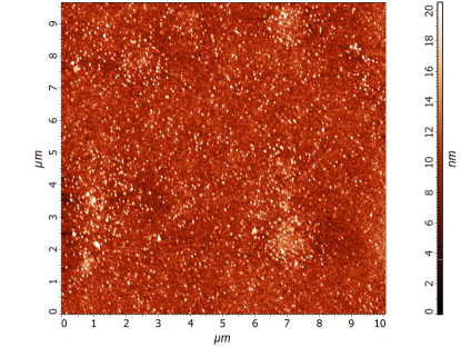
The film inhomogeneity in Fig. 4 occurs due to the thickness variation around the film, which is demonstrated in Fig. 5 by atomic-force technique. The bottom layers of the film are filled completely, while the upper layer consists from the coagulated regions. The resulting thickness variation leads to the pattern of percolation clusters for the current flow. In this case the resistance between two sample contacts is determined by several percolation channels, which are connected in parallel. Thick sections of the sample in Fig. 4 form the conducting clusters while the resistance is mostly determined by the critical regions of small thicknesses between these clusters shklovskii .
In the case of percolation current flow, conductivity is increasing at high voltage biases, which is usually explained by the breakdown of the resistive sections shklovskii . The conductivity no longer depends on specific geometric dimensions of highly resistive area of a particular percolation channel when the field strength value (where m is a sample length) allows for an electron to achieve the mobility edge by obtaining an energy at the characteristic localization length . Because of the large number of clusters of different sizes in strongly disordered antimony films, there is no certain breakdown voltage for the experimental curves, so we observe smooth increase of conductivity with voltage bias. At high biases, the conductivity becomes independent of the particular configuration of resistive regions, which leads to the coincidence of curves at large values, as it can be seen in the inset to Fig. 2 (b).
The described mechanism is independent of a bias sign, which well corresponds to symmetric (i.e. even) curves. On the other hand, the existence of two distinct values of conductivity at zero bias indicates modification of the percolation pattern. Since the modification is sensitive to the bias sign, it is only possible due to charging of some film regions theory .
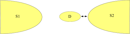
Really, resistance of the percolation channel is determined by the most resistive area situated between two conductive regions percolation . For strongly disordered samples, for some of the channels, it is natural to expect that there is a small cluster (i.e. large quantum dot, electron trap) weakly coupled to the conductive regions, see Fig. 6. The coupling strengths are obviously not equivalent due to the arbitrary location of the cluster. When a high bias is applied between the regions S1 end S2, this cluster (trap) is charged or discharged, depending on the bias sign. The charging/discharging process goes through the breakdown to the nearest conductive region (D-S2 in Fig. 6), so it requires finite breakdown voltage (see above). As a result, the cluster (trap) charging (or discharging) is accompanied by redistribution of the electron density in the conductive regions, due to the screening effects shklovskii . Thus, the cluster (trap) state "charged/uncharged" determines the configuration the most resistive area in the percolation channel, i.e. the value of the sample differential resistance at zero bias. Since the trap charging/discharging requires finite voltage, an actual configuration of the percolation channels is stable at zero bias, which is revealed in the relaxation curves in Fig. 3. In principle, similar recharge process has been predicted theoretically theory .
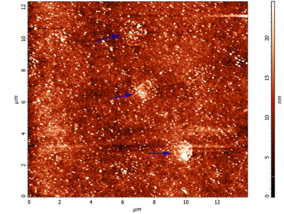
Small clusters (electron traps) can be realized, e.g., as small crystalline inclusions in the amorphous film, see Fig. 7. It demonstrates inclusions of a round shape (marked by arrows) in topography AFM scan of the film area between the Ohmic contacts. These inclusions have sharp boundaries, they appear by 2 nm above the surface in profile. The inclusions can be regarded as clusters of the crystalline phase in the amorphous film butenko and are of 0,5-1,5m in size.
V Conclusion
In conclusion, we study conductivity of strongly disordered amorphous antimony films under high bias voltages. We observe non-linear current-voltage characteristic, where the conductivity value at zero bias is one of two distinct values, being determined by the sign of previously applied voltage. Relaxation curves demonstrate high stability of these conductivity values on a large timescale. Investigations of the antimony film structure allows to determine the percolation character of electron transport in strongly disordered films. We connect the memory effect in conductivity with modification of the percolation pattern due to recharging of some film regions at high bias voltages.
VI Acknowledgement
The authors are grateful to A.M. Ionov for fruitful discussions, S.V. Chekmazov for technical assistance, E.Yu. Postnova for electron microscopy, S.S. Khasanov for X-ray sample characterization, and V.M. Chernyak for preparation of amorphous films. We gratefully acknowledge financial support partially by the RFBR (project No. 19-29-03021), and RF State task.
References
- (1) M. Prezioso, F. Merrikh-Bayat, B.D. Hoskins, G.C. Adam, K.K. Likharev, and D.B. Strukov, Nature 521, 61 (2015).
- (2) G.W. Burr, R.M. Shelby, A. Sebastian, S. Kim, S. Kim, S. Sidler, K. Virwani, M. Ishii, P. Narayanan, A. Fumarola, L.L. Sanches, I. Boybat, M. Le Gallo, K. Moon, J. Woo, H. Hwang, and Y. Leblebici, Advances in Physics-X 2 (1), 89 (2017).
- (3) L. O. Chua, IEEE Trans. Circuit Theory 18, 507-519 (1971).
- (4) M. Di Ventra and Y. V. Pershin, Nanotechnology 24, 255201 (2013).
- (5) Q. Xia, J.J. Yang, Nature Materials, 18, 309 (2019).
- (6) N.A. Tulina, A.A. Ivanov, A.N. Rossolenko, I.M. Shmytko, A.M. Ionov, R.N. Mozhchil, S.I. Bozhko, I.Yu. Borisenko, V.A. Tulin, Materials Letters, 203, 97, (2017).
- (7) A. S. Vedeneev, V. A. Luzanov and V. V. Rylkov, JETP Letters 109, 171 (2019)
- (8) H.-S. P. Wong, S. Raoux, S. Kim, J. Liang, J. P. Reifenberg, B. Rajendran, M. Asheghi, and K. E. Goodson, Proceedings of the IEEE, Vol. 98, (2010)
- (9) V.T. Dolgopolov, Phys. Usp. 62 633–648 (2019); DOI: 10.3367/UFNe.2018.10.038449
- (10) V.F. Gantmakher, V.T. Dolgopolov, Phys. Usp. 51 3–22 (2008); DOI: 10.1070/PU2008v051n01ABEH006471
- (11) B.I. Shklovskii, A.L. Efros, Electronic Properties of Doped Semiconductors (Springer, New York, 1984).
- (12) Kunisuke Maki, Jpn. J. Appl. Phys., 13649 (1974)
- (13) Mituru Hashimoto et al., Jpn. J. Appl. Phys. 19, 21 (1980).
- (14) R.C. Fischer, in Encyclopedia of Inorganic and Bioinorganic Chemistry, by John Wiley and Sons, Ltd. (2016) DOI: 10.1002/9781119951438.eibc0011.pub2
- (15) L.S. Palatnik, M.Ya. Fuks, V.M. Kosevich, Mechanism of formation and substructure of condensed films, (1972) Moscow, Nauka publ., (In Russian)
- (16) A.V. Butenko, E.I. Bukhshtab, JETP, Vol. 61, No. 3, p. 618 (1985)
- (17) R.F. Mamin, JETP Letters, 52, 335 (1984)
- (18) A.E. Morozovskii, A.A. Snarskii, JETP, Vol. 77, No. 6, p. 959 (1993)