Superconducting microwire detectors with single-photon sensitivity in the near-infrared
Abstract
We report on the fabrication and characterization of single-photon-sensitive WSi superconducting detectors with wire widths from 1 µm to 3 µm. The devices achieve saturated internal detection efficiency at 1.55 µm wavelength and exhibit maximum count rates in excess of 105 s-1. We also investigate the material properties of the silicon-rich WSi films used for these devices. We find that many devices with active lengths of several hundred microns exhibit critical currents in excess of 50% of the depairing current. A meandered detector with 2.0 µm wire width is demonstrated over a surface area of 362 362 µm2, showcasing the material and device quality achieved.
Superconducting nanowire single-photon detectors (SNSPDs) Gol’tsman et al. (2001); Holzman and Ivry (2019) have become invaluable in a broad range of applications thanks to their superior detection efficiency Marsili et al. (2013a); Esmaeil Zadeh et al. (2017); Smirnov et al. (2018); Reddy et al. (2019), low dark count rates Hochberg et al. (2019), and ease of integration with integrated photonic circuits Buckley et al. (2017); McDonald et al. (2019). Thanks to the small superconducting energy gap of many films used in these devices, they can exhibit a large optical detection bandwidth reaching out to the mid-IR Marsili et al. (2012, 2013b); Chen et al. (2018); Verma et al. (2019). Typically, wire widths on the order of 100 nm are necessary to achieve saturated internal detection efficiency (IDE) in the infrared. However, recent experiments by Korneeva et al. have shown that microbridge-type MoSi superconducting detectors can exhibit single-photon sensitivity up to = 1 µm for wire widths of 1 µm Korneeva et al. (2018a). It is thought that a prerequisite for this behavior is a high material homogeneity and minimal geometric constrictions in the device, permitting bias currents close to the intrinsic depairing current of the unpatterned film Vodolazov (2017); Korneeva et al. (2018b), at which point a hotspot generated in a detection event can lead to a normal region across the entire wire, independent of the wire width. Simultaneously, the superconducting gap of the material also affects the number of Cooper pairs broken in an absorption event, leading to more efficient detection for wide wires with a lower-gap material. Exploiting these two behaviors would enhance the competitiveness of SNSPDs fabricated with photolithography Shainline et al. (2017), allowing high-yield production in a parallel process. Furthermore, wide wires on the micron scale would naturally carry much more current and enhance the signal generated from a detection event (although trade-offs for modifying the superconducting gap must also be considered), potentially reducing the cost and complexity of the electronics that are required per detector channel. A larger signal, in general, also leads to lower jitter for nanowire detectors.
While the results in Ref. Korneeva et al., 2018a are highly encouraging and have stimulated new interest in exploring the physics of detection events in SNSPDs, there are significant caveats. One is that a detection efficiency plateau is not observed for wavelengths longer than 1 µm, and the other is that the devices demonstrated to date are still only short bridges, suggesting that the intrinsic material inhomogeneity is still a limiting factor in realizing reliable ‘microwire’ devices. The study of microwire devices would benefit from parallel efforts in alternative amorphous superconducting materials such as WxSi1-x, which exhibits high material homogeneity allowing excellent yield and consistent performance across many devices. Recently, we demonstrated kilopixel detector arrays with yield > 99% Wollman et al. (2019). In this manuscript, we fabricate microwire and nanowire devices in several WSi films of different stoichiometry and thickness and compare their performance. We also study the fundamental material properties of these films. We demonstrate saturated IDE at = 1.55 µm in out-and-back microwire detectors with wire widths up to 3 µm and wire lengths of 100 µm, as well as in meandered microwire devices (2 µm wire width) over a detector area of 362 362 µm2 (10,000 squares of wire). For contrast, the typical size of meandered detectors is on the order of 15 15 µm2.
We considered several variations on film properties in the process of fabricating and testing devices used in this work. In the process of optimizing a film for a given application, the superconducting energy gap is often tailored to optimize or trade-off the superconducting transition temperature (Tc), the critical current density, and the sensitivity to long-wavelength photons Verma et al. (2019); Zichi et al. (2019). In the case of WSi, the superconducting energy gap can be reduced by increasing the fraction of silicon in the film, and reducing the thickness. In this work, we compare four types of WSi films in a 2 2 matrix: either 260 W or 320 W of sputtering power applied during sputtering of the silicon, and a deposited film thickness of either 2.1 nm or 2.8 nm. The film properties are compared in Table 1.
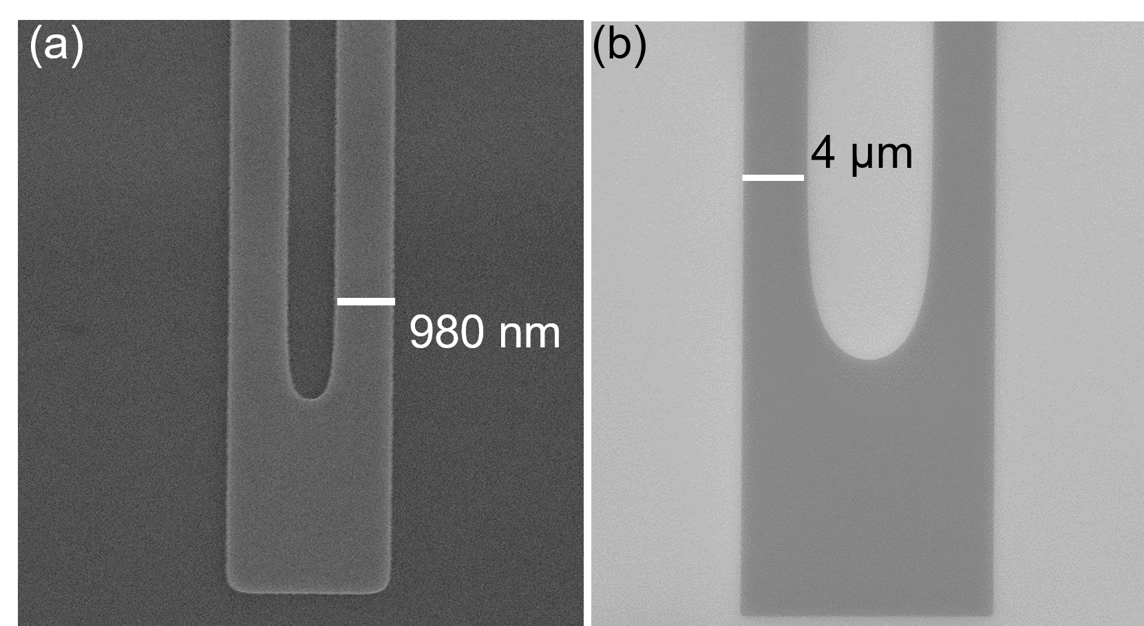
The devices were fabricated at the 76-mm-diameter wafer scale by depositing WSi onto a silicon wafer with 160 nm thermal oxide, followed by lithographic patterning and plasma etching with dilute SF6 in Ar. The wafer was then diced into 1 cm-square chips which were wire-bonded to sample mounts and cooled to 750-800 mK. Most of the devices were patterned with conventional 365 nm photolithography, except for a final fabrication run conducted with electron-beam (e-beam) lithography for the 3S-type film. An example microwire out-and-back device after fabrication is shown in Fig. 1(a). The various device geometries used in this manuscript are also shown in the insets of Fig. 4(a-c): straight wire, out-and-back, and meander. On-chip meandered inductors (with wires significantly wider than the width of the device under test) are used to prevent latching.
| Sample name | 2S | 2L | 3S | 3L |
|---|---|---|---|---|
| Thickness (nm) | 2.1 | 2.8 | 2.1 | 2.8 |
| Si mol. frac. | 0.36 | 0.36 | 0.48 | 0.48 |
| Tc (K) | 3.2 | 3.5 | 2.9 | 3.3 |
| 0 (meV) | 0.49 | 0.53 | 0.44 | 0.50 |
| Lk,exp. (pH/) | 280 | 190 | 420 | 230 |
| Jdep (MA/cm2) | 1.5 | - | 1.2 | - |
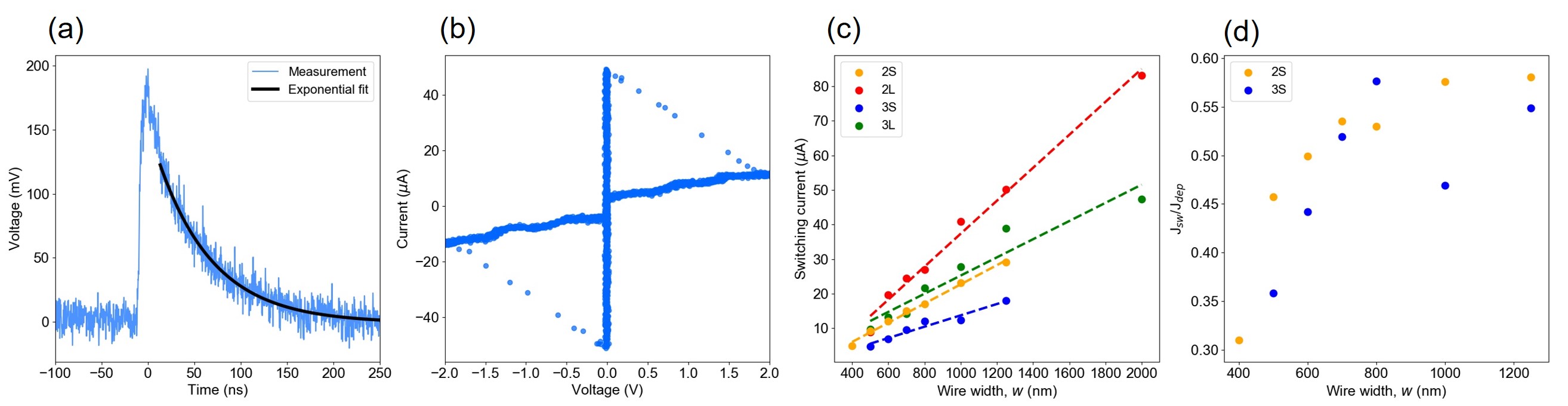
For each sample type, we conducted measurements on the as-deposited films to determine various intrinsic properties, summarized in Table 1. The critical temperature is defined here as the temperature at which the sheet resistance of the film reaches 50% of the sheet resistance at 20 K. The film stoichiometry was determined by secondary ion mass spectroscopy. The kinetic inductance was determined by fitting a single-exponential decay to the voltage response of the detector, as shown in Fig. 2(a).
Before testing the photon-detection performance, we characterized the critical current performance of the devices and different films. An example I-V curve is plotted in Fig. 2(b). We performed I-V sweeps for wire widths from 400 nm to 1250 nm and for all four sample types; the switching current results are collected in Fig. 2(c). While they mostly follow linear fits to the nanowire width as one would expect, it is clear that some deviation from the ideal values is present when the data are instead normalized to the depairing current density, as in Fig. 2(d) for samples 2S and 3S. In both cases, the ratio of switching current density to depairing current density is lower for wire widths of < 700 nm, but mostly saturates for larger wires, most likely due to small constrictions from photolithographic patterning. Regardless, the wider devices exhibit > 0.55, despite the significant total wire length of 400 µm and the presence of a hairpin turn in the device structure.
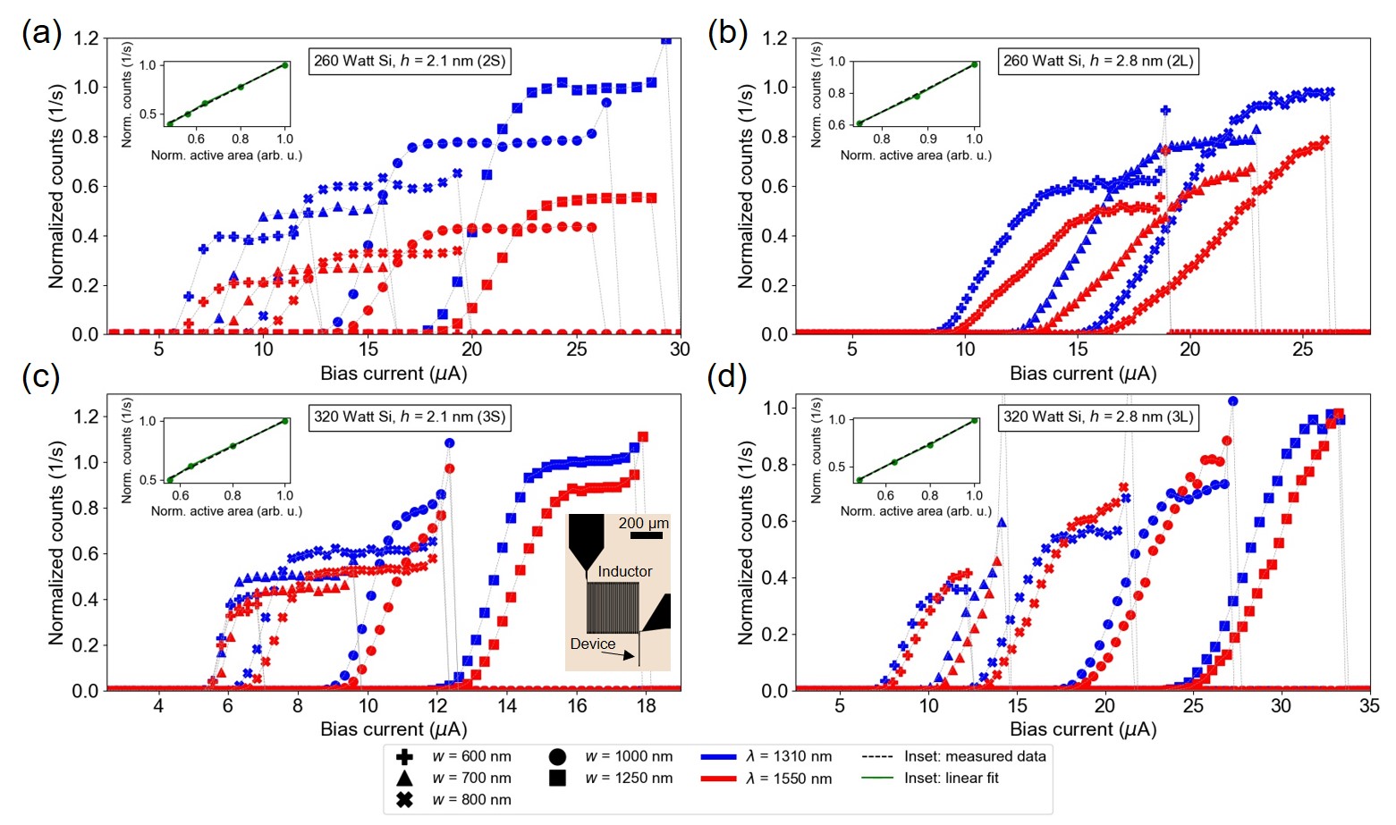
Next, we characterized the photon detection performance of out-and-back detectors for wire widths up to 1250 nm and a fixed total wire length of 400 µm, for all four film types (Fig. 3(a-d)). The geometry is shown in the inset of Fig. 3(a). Flood illumination was used to characterize the device responses to photons at 1310 nm and 1550 nm. A typical count rate of s-1 was recorded during these measurements. Rates varied somewhat between samples due to non-uniform illumination, and are normalized in this particular measurement to allow their straightforward comparison. For films 2S, 2L and 3S, good plateaus in the IDE are seen for = 1310 nm for most wire widths in the range that we tested, and films 2S and 3S exhibited plateaus at 1550 nm as well. Comparing the thinner to the thicker films, it suggests the reduced thickness is quite beneficial to photon detection performance in wide wires here, which is reasonable to expect given the change in superconducting energy gap.
So far in this work, we have only examined microwire devices with widths up to 1.25 µm. We also fabricated much wider microwire devices in both straight wire and out-and-back configurations (see insets of Fig. 4 for visual reference). Devices had widths from 1 µm to 4 µm. A separate fabrication run was conducted using the 3S-type film and e-beam patterning. The measurement results of all devices from this run are collected in Fig. 4. Note that a slightly lower Tc of 2.5 K was seen in this sample due to temporary issues with the deposition system, but wide devices made on the previous 3S-type film also showed similar saturation curve results. First, we consider the photon detection performance of straight microwires in Fig. 4(a) of lengths of 65 µm. Under 1550 nm illumination, the 3 µm and 4 µm-wide devices achieve a plateau-like region with a small linear slope that is likely due to counts in the tapers connecting the device to the bond-pad and inductor. For the out-and-back type devices (Fig. 4(b)) with a longer total length of about 100 µm, we observed a clear plateau in the IDE under 1550 nm illumination for a wire width of 3 µm. For the 4 µm wide out-and-back device, the count rate is seen to just begin to flatten although a clear plateau is not observed. The final device geometry tested was meandered detectors. Fig. 4(c) shows the photon counting performance for several such detectors, with widths of 1, 1.5 and 2 µm and fill fractions of 30% or 50%. All these devices show a clear plateau in their response to 1550 nm light despite wire lengths of 10,000 squares. In the case of the 2 µm wide-wire meander occupying 362 362 µm2, its surface area is 0.13 mm2. Finally, to confirm that the measurements of microwires was performed in a linear regime, we tested a 2 µm wide out-and-back device of 100 µm total length with variable optical attenuation (Fig. 4(d)). The count rate is highly linear for count rates of s-1 to s-1.
In conclusion, we report the fabrication and characterization of single-photon-sensitive microwire detectors with widths ranging from 1 µm to 3 µm and lengths ranging from 65 µm to 20,000 µm. The material properties of different WSi film thicknesses and stoichiometries are compared to motivate and explain the performance we achieve in the experiments. A meandered detector with a wire width of 2 µm and an area of 362 362 µm2 is shown to have saturated IDE at = 1550 nm, demonstrating that the fabrication process and the material homogeneity are both sufficiently high-quality for state-of-the-art detector fabrication in this platform. These results have implications for the high-volume production of large-area single-photon detectors with potential applications in dark matter detection Hochberg et al. (2019), single-photon optical metrology Fox (1991), and imaging arrays Wollman et al. (2019).
Acknowledgements.
We thank Karl K. Berggren and Ilya Charaev at MIT for helpful discussions. This is a contribution of NIST, an agency of the U.S. government, not subject to copyright.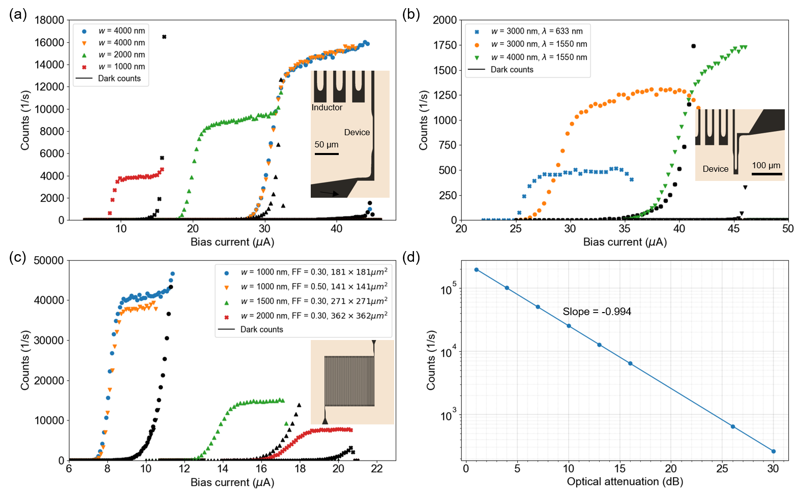
References
- Gol’tsman et al. (2001) G. N. Gol’tsman, O. Okunev, G. Chulkova, A. Lipatov, A. Semenov, K. Smirnov, B. Voronov, A. Dzardanov, C. Williams, and R. Sobolewski, “Picosecond superconducting single-photon optical detector,” Applied Physics Letters 79, 705–707 (2001).
- Holzman and Ivry (2019) I. Holzman and Y. Ivry, “Superconducting Nanowires for Single-Photon Detection: Progress, Challenges, and Opportunities,” Adv. Quant. Technol. 2, 1800058 (2019).
- Marsili et al. (2013a) F. Marsili, V. B. Verma, J. A. Stern, S. Harrington, A. E. Lita, T. Gerrits, I. Vayshenker, B. Baek, M. D. Shaw, R. P. Mirin, and S. W. Nam, “Detecting single infrared photons with 93% system efficiency,” Nature Photonics 7, 210 (2013a).
- Esmaeil Zadeh et al. (2017) I. Esmaeil Zadeh, J. W. N. Los, R. B. M. Gourgues, V. Steinmetz, G. Bulgarini, S. M. Dobrovolskiy, V. Zwiller, and S. N. Dorenbos, “Single-photon detectors combining high efficiency, high detection rates, and ultra-high timing resolution,” APL Photonics 2, 111301 (2017).
- Smirnov et al. (2018) K. Smirnov, A. Divochiy, Y. Vakhtomin, P. Morozov, P. Zolotov, A. Antipov, and V. Seleznev, “NbN single-photon detectors with saturated dependence of quantum efficiency,” Superconductor Science and Technology 31, 35011 (2018).
- Reddy et al. (2019) D. V. Reddy, R. R. Nerem, A. E. Lita, S. W. Nam, R. P. Mirin, and V. B. Verma, “Exceeding 95% system efficiency within the telecom C-band in superconducting nanowire single photon detectors,” in Conference on Lasers and Electro-Optics, OSA Technical Digest (Optical Society of America, San Jose, California, 2019) p. FF1A.3.
- Hochberg et al. (2019) Y. Hochberg, I. Charaev, S.-W. Nam, V. Verma, M. Colangelo, and K. K. Berggren, “Detecting dark matter with superconducting nanowires,” arXiv preprint arXiv:1903.05101 (2019).
- Buckley et al. (2017) S. Buckley, J. Chiles, A. N. McCaughan, G. Moody, K. L. Silverman, M. J. Stevens, R. P. Mirin, S. W. Nam, and J. M. Shainline, “All-silicon light-emitting diodes waveguide-integrated with superconducting single-photon detectors,” Applied Physics Letters 111, 141101 (2017).
- McDonald et al. (2019) C. McDonald, G. Moody, S. W. Nam, R. P. Mirin, J. M. Shainline, A. McCaughan, S. Buckley, and K. L. Silverman, “Iii-v photonic integrated circuit with waveguide-coupled light-emitting diodes and wsi superconducting single-photon detectors,” Applied Physics Letters 115, 081105 (2019), https://doi.org/10.1063/1.5108893 .
- Marsili et al. (2012) F. Marsili, F. Bellei, F. Najafi, A. E. Dane, E. A. Dauler, R. J. Molnar, and K. K. Berggren, “Efficient Single Photon Detection from 500 nm to 5 m Wavelength,” Nano Letters 12, 4799–4804 (2012).
- Marsili et al. (2013b) F. Marsili, V. B. Verma, M. J. Stevens, J. A. Stern, M. D. Shaw, A. J. Miller, D. Schwarzer, A. Wodtke, R. P. Mirin, and S. W. Nam, “Mid-infrared single-photon detection with tungsten silicide superconducting nanowires,” in CLEO: 2013 (2013) pp. 1–2.
- Chen et al. (2018) L. Chen, D. Schwarzer, J. A. Lau, V. B. Verma, M. J. Stevens, F. Marsili, R. P. Mirin, S. W. Nam, and A. M. Wodtke, “Ultra-sensitive mid-infrared emission spectrometer with sub-ns temporal resolution,” Optics Express 26, 14859–14868 (2018).
- Verma et al. (2019) V. B. Verma, A. E. Lita, B. Korzh, E. Wollman, M. D. Shaw, R. P. Mirin, and S. W. Nam, “Towards single-photon spectroscopy in the mid-infrared using superconducting nanowire single-photon detectors,” in Proc.SPIE, Vol. 10978 (2019).
- Korneeva et al. (2018a) Y. Korneeva, D. Vodolazov, I. Florya, N. Manova, E. Smirnov, A. Korneev, M. Mikhailov, G. Goltsman, and T. M. Klapwijk, “Single photon detection in micron scale NbN and -MoSi superconducting strips,” EPJ Web Conf. 190 (2018a).
- Vodolazov (2017) D. Vodolazov, “Single-Photon Detection by a Dirty Current-Carrying Superconducting Strip Based on the Kinetic-Equation Approach,” Physical Review Applied 7, 34014 (2017).
- Korneeva et al. (2018b) Y. Korneeva, D. Vodolazov, A. Semenov, I. Florya, N. Simonov, E. Baeva, A. Korneev, G. Goltsman, and T. Klapwijk, “Optical Single-Photon Detection in Micrometer-Scale NbN Bridges,” Physical Review Applied 9, 64037 (2018b).
- Shainline et al. (2017) J. M. Shainline, S. M. Buckley, N. Nader, C. M. Gentry, K. C. Cossel, J. W. Cleary, M. Popović, N. R. Newbury, S. W. Nam, and R. P. Mirin, “Room-temperature-deposited dielectrics and superconductors for integrated photonics,” Optics Express 25, 10322–10334 (2017).
- Wollman et al. (2019) E. E. Wollman, V. B. Verma, A. E. Lita, W. H. Farr, M. D. Shaw, R. P. Mirin, and S. W. Nam, “A kilopixel array of superconducting nanowire single-photon detectors,” arXiv preprint arXiv:1908.10520 (2019).
- Zichi et al. (2019) J. Zichi, J. Chang, S. Steinhauer, K. von Fieandt, J. W. N. Los, G. Visser, N. Kalhor, T. Lettner, A. W. Elshaari, I. E. Zadeh, and V. Zwiller, “Optimizing the stoichiometry of ultrathin NbTiN films for high-performance superconducting nanowire single-photon detectors,” Optics Express 27, 26579–26587 (2019).
- Fox (1991) N. Fox, “Trap detectors and their properties,” Metrologia 28, 197 (1991).
- Natarajan, Tanner, and Hadfield (2012) C. M. Natarajan, M. G. Tanner, and R. H. Hadfield, “Superconducting nanowire single-photon detectors: physics and applications,” Superconductor Science and Technology 25, 63001 (2012).