Epitaxial Pb on InAs nanowires
Abstract
Semiconductor-superconductor hybrids are widely used for realising complex quantum phenomena such as topological superconductivity and spins coupled to Cooper pairs. Accessing exotic regimes at high magnetic fields and increasing operating temperatures beyond the state-of-the-art requires new, epitaxially matched semiconductor-superconductor materials. The challenge is to generate favourable conditions for heterostructure formation between materials with the desired inherent properties. Here, we harness increased knowledge of metal-on-semiconductor growth to develop InAs nanowires with epitaxially matched, single crystal, atomically flat Pb films along the entire nanowire. These highly ordered heterostructures have a critical temperature of 7 K and a superconducting gap of 1.25 meV, which remains hard at T, thereby more than doubling the available parameter space. Additionally, InAs/Pb ‘island’ devices exhibit magnetic field-driven transitions from Cooper pair to single electron charging; a pre-requisite for use in topological quantum computation. Introducing semiconductor-Pb hybrids potentially enables access to entirely new regimes for an array of quantum systems.
The development of high-quality semiconductor-superconductor heterostructures underlies the pursuit of new types of quantum bits based on exotic physics arising at the hybrid interface lutchyn2018majorana ; krogstrup2015epitaxy ; mourik2012signatures ; DasNatPhys12 ; Deng2012NL ; deng2016majorana ; ZhangNature18 ; PendharkarTinArxiv ; KlinovajaPRB2014 . Aside from the ability to host novel two-level systems LarsenPRL15 ; LuthiPRL18 ; TosiPRX2019 ; HaysPRL2019 ; PradaarXiv2019 , when the underlying materials exhibit strong spin-orbit coupling, a high -factor and ‘hard gap’ induced superconductivitychang2015hard , they are ideally suited for supporting topological superconductivity under applied magnetic fieldOregPRL10 ; LutchynPRL10 ; mourik2012signatures ; deng2016majorana ; albrecht2016exponential ; DasNatPhys12 ; Deng2012NL ; lutchyn2018majorana ; PradaarXiv2019 . Signatures of topological superconductivity in these systems have been studied almost exclusively using InAs or InSb as the semiconductor and Al and Nb(TiN) as the superconductor, with the large spin-orbit coupling and -factor ensuring the suitability of these semiconductorslutchyn2018majorana . By contrast, there is strong interest in improving the superconductor material to broaden the scope of hybrid applicationsCarradArXiv191100460Cond-Mat2019 ; bjergfelt2019superconducting ; PendharkarTinArxiv , since Al has a relatively low critical temperature, and field chang2015hard , while the soft gap of Nb-based hybrids has thus far prevented isolated hybrid segments supporting Cooper pair charging albrecht2016exponential ; CarradArXiv191100460Cond-Mat2019 ; shen2018parity ; PendharkarTinArxiv ; Vaitiekenasfullshell18 ; a crucial requirement for topologically protected qubit schemesAasenPRX16 . The main goal is therefore development of epitaxial hybrids exhibiting a large, hard gap resilient to high magnetic fields and elevated temperaturesCarradArXiv191100460Cond-Mat2019 ; bjergfelt2019superconducting ; PendharkarTinArxiv .
In this article we present hybrid nanowires utilising Pb as the superconductor, which possesses the highest bulk and of all elemental type-I superconductors, vastly extending the hybrid parameter space. We deposit the Pb films without breaking vacuum after InAs nanowire growthkrogstrup2015epitaxy ; GuskinNanoscale17 ; CarradArXiv191100460Cond-Mat2019 ; bjergfelt2019superconducting , and ensure carefully controlled conditions which promote strong thermodynamic driving forces towards single crystal formation. From transmission electron microscopy (TEM) we find a low energy domain match, as expected from modelling of the InAs/Pb interface, which enables the growth of an atomically flat single Pb crystal along the entire nanowire facet. All previous semiconductor-superconductor nanowire heterostructures exhibited axial grain boundaries and/or polycrystallinitykrogstrup2015epitaxy ; GuskinNanoscale17 ; CarradArXiv191100460Cond-Mat2019 ; bjergfelt2019superconducting ; PendharkarTinArxiv . The single crystal Pb suppresses the potential for impurity-generated discontinuity of the hybrid wavefunctiondeng2016majorana , which may occur in granular filmsGuskinNanoscale17 ; CarradArXiv191100460Cond-Mat2019 ; bjergfelt2019superconducting ; PendharkarTinArxiv . Further, the theoretical description used to optimise the epitaxial structures through consideration of thermodynamic driving forces and structural factors leads to increased understanding of metal/semiconductor epitaxy. The epitaxial InAs/Pb structure yields a hard induced superconducting energy gap of meV, corresponding K, and exceeding T, the highest reported values for epitaxial semiconductor-superconductor hybrids. In addition, InAs/Pb ‘island’ devices support Cooper pair charging due to the hard gap. At finite magnetic field, this evolves into single electron transport through a hybrid bound statealbrecht2016exponential ; shen2018parity ; CarradArXiv191100460Cond-Mat2019 ; Vaitiekenasfullshell18 ; sestoft2018engineering ; PendharkarTinArxiv ; a crucial feature in the context of topological quantum computation. The epitaxial structure and dramatic enhancement of the accessible parameter space represented by InAs/Pb hybrids make them prime candidates for use in a wide range of semiconductor-superconductor hybrids based on nanowiresmourik2012signatures ; deng2016majorana ; LarsenPRL15 ; TosiPRX2019 ; LuthiPRL18 , selective area grown networksVaitiekenasPRL18sag ; AseevNL18 , and planar heterostructuresKjaergaardNatComm16 ; ShabaniPRB2016 . Further, Pb possesses features that distinguish it from other elemental superconductors, such as two-band, strong-coupling superconductivity and a large spin-orbit coupling, which may lead to the emergence of new phenomena in semiconductor-superconductor physics lutchyn2018majorana ; PradaarXiv2019 ; SauNatComm2012 ; SuNatCommun2017 ; KlinovajaPRB2014 ; LarsenPRL15 ; TosiPRX2019 .
InAs/Pb epitaxy
Aside from the attractive physical properties, the choice of Pb was based on analytical considerations of the central stages in metal film growth on different semiconductor nanowires. To do this, we theoretically assessed structural stability in combination with estimates of the interplay between the four contributions to the overall excess energy, which determine the thermodynamic driving forces and kinetic limiting factors. A full description is given in Supplementary Section 1 and an additional 12 elemental superconductors on InAs nanowires are theoretically studied in Supplementary Section 2. For low temperature depositions ( K) it is energetically favourable for Pb to grow in a single crystallographic orientation with respect to InAs. Combined with the high grain boundary mobility of Pb, this suggests that growth of Pb on InAs would result in large crystals with an epitaxial match to the nanowire. In contrast, epitaxial Al grows in 2 or 4 orientations on InAs depending on thicknesskrogstrup2015epitaxy , and other superconductor materials employed so far feature no long-range orderCarradArXiv191100460Cond-Mat2019 ; bjergfelt2019superconducting ; GuskinNanoscale17 ; PendharkarTinArxiv , consistent with our findings in Supplementary Section 2. These findings suggest Pb as the optimal elemental superconductor material to combine with InAs. Although we focus on InAs/Pb nanowires in this article, we note that Pb will likely match well to other semiconductors (see Supplementary Section 3.1), and our results should translate to planar heterostructuresShabaniPRB2016 ; KjaergaardNatComm16 and selective area grown networksVaitiekenasPRL18sag ; AseevNL18 . Further, the framework presented in Supplementary Section 1 is instructive in developing the range of semiconductor-metal epitaxial structures.
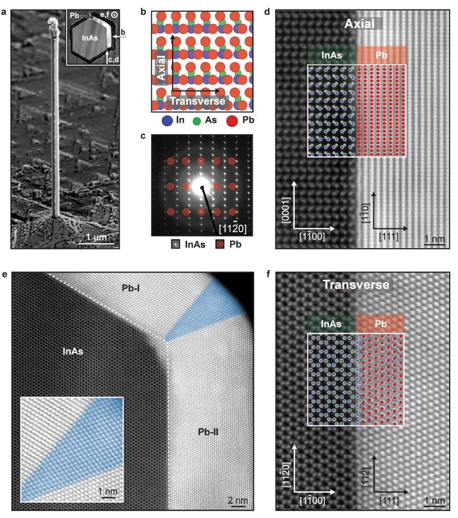
Figure 1a shows a scanning electron microscope (SEM) micrograph of a hexagonal InAs nanowire with Pb deposited on two facets. The wurtzite InAs nanowires were grown along the direction using molecular beam epitaxy (MBE), with flat facets. The hexagonal morphology was optimised as outlined in Methods and Supplementary Section 3. After the nanowires were grown the wafer was transferred without breaking ultra-high vacuum to a second chamber where the substrate was placed on a liquid nitrogen cooled substrate holder, K, for several hours, before Pb was deposited using e-beam evaporationCarradArXiv191100460Cond-Mat2019 ; bjergfelt2019superconducting ; GuskinNanoscale17 . The inset in Figure 1a shows a low magnification high angle annular dark field scanning transmission electron microscope (HAADF STEM) micrograph of a cross-sectioned InAs/Pb/Si heterostructure. Figure 1a shows the modeled relaxed hetero-epitaxial match along (InAs)/ (Pb) directions and the arrows indicate the axial and transverse direction. Figure 1c shows a selected area electron diffraction (SAED) pattern of an entire nanowire, oriented along the / direction parallel to the nanowire facet. Notably, only one Pb orientation relative to the InAs nanowire facet is observed (red circles), confirming the theoretical hypothesis that a Pb thin film forms a single crystal along an entire nanowire facet.
Figure 1d shows a high resolution (HR) HAADF STEM micrograph of the InAs/Pb interface where the orientation is similar to that of Fig. 1c. The inset in Fig. 1d shows how the theoretically predicted strain relaxed hetero-epitaxial match fits to the observed interface. From this, a particularly small bi-crystal interfacial domain is found along the / nanowire growth direction, with two planes of Pb for each plane of InAs and a bulk residual mismatch of only . From HR TEM investigations of the entire nanowire length no edge-dislocations were found, indicating that the small strain needed to obtain the epitaxial domain is absorbed. Figure 1e presents a HAADF STEM micrograph of the cross-sectioned InAs/Pb nanowire shown in Fig. 1a (inset). The two grains (, ) form single crystals along their entire nanowire facet, and are merged by a wedge-shaped single-crystalline domain, false coloured blue. The inset in Figure 1e shows how the wedge-shaped grain accommodates two coherent grain boundaries and thus reduces the grain boundary energy between the single and crystals. Strain in InAs and Pb along the transverse direction is observed by comparing the STEM micrograph and the predicted strain relaxed hetero-epitaxial match in Figure 1f. By utilizing the average [] plane spacing as a scale to measure the relative stress in the structure, Pb along the [] direction was measured to be compressively strained 1.7 % whereas InAs along [] direction was found to be tensile strained 0.7 %. Assuming that the InAs [] planes are not heavily influenced by the interface, the compressed Pb and expanded InAs indicate that the transverse bi-crystal interfacial match seeks a domain of two interface planes of InAs for three planes of Pb. More detail is provided in Supplementary Section 3. The presented single crystal nature and epitaxial relation relative to the InAs nanowire facets was found for all investigated Pb thicknesses (5-60 nm) and Pb thus appears robust against stress driven terms such as incoherent grain boundaries.
To study the Pb film morphology, surface sensitive scanning electron microscopy (SEM) micrographs of InAs/Pb hybrids are shown in Figs 2a,c,e for 15, 30 and 60 nm Pb films, respectively. Patterning of the Pb coatings was implemented to enable comparative analysis of core/shell morphology and achieved by adjacent nanowires acting as shadow masks during Pb depositionkrizek2017growth ; gazibegovic2017epitaxy ; PendharkarTinArxiv . Figure 2b,d,f show bright field TEM micrographs for the different Pb thicknesses, and Fig. 2g shows a HR TEM micrograph of the terminating planes of a 15 nm film of Pb marked with a red square in Fig. 2b. The Pb morphology is continuous and atomically flat for most of the investigated film thicknesses (10 nm - 30 nm). However, above a critical thickness (in our case 50 nm), dependent on the growth conditions, the surface becomes more rough (Fig. 2e). In Fig. 2f, bending contours and contrast changes are observed, indicative of strain fields in the Pb film. This may be caused by the increased strain imposed by the grain boundaries between the adjacent facets or a slight bending of the nanowires, likely due to either thermal expansion coefficient differences or axial strain krogstrup2015epitaxy ; bjergfelt2019superconducting .
Obtaining a single crystal superconductor on a single crystal semiconductor is critical for hybrid and topological applications to ensure that each end of e.g. the topological system coincides with the geometrically defined end of the superconducting segment, rather than at an impuritydeng2016majorana . Achieving the structures presented here required detailed understanding of how to control and promote epitaxial growth, via thermodynamic and grain growth kinetics considerations. We focus specifically on Pb, with more general explanations provided in Supplementary Section 1-3. The aim during the initial phase of Pb thin film growth is to promote layer-by-layer-like growth. For island growth this is achieved by decreasing the critical cluster size and thereby increasing the initial concentration of critical clusters pentcheva2003non . Experimentally, this was done by lowering the substrate temperature and increasing the material flux. After the initial clusters have been established they start to grow. In this phase, interface and strain energy may result in recrystallization of the clusters in a kinetically limited process due to the thermodynamic driving forces. In a later stage the clusters start to impinge and coalesce into a single crystal, which is now strongly dependent on the main contributions to the overall excess energy venables1983nucleation ; vesselinov2016crystal . We find that it is especially important to have very well defined nanowire facets to decrease the interface and strain energy (Supplementary Section 1.1). The micrographs in Figs 2a,c suggest that after a continuous film of Pb has grown, the growth switches to layer-by-layer mode. Here, small islands on the completed atomically flat layer act as nucleation sites for the next layer. Upon warming to room temperature and subsequent exposure to oxygen there is a chance that the Pb thin film dewets since it grows far from thermodynamic equilibrium thompson2012solid . We find that the film morphology is improved when the substrate remains on the cold holder for approximately 10 hours after terminating growth. Dewetting and oxidiation of Pb thin films may also be prevented by growing a capping layer with a lower dewetting probability.
Tunneling spectroscopy of InAs/Pb junctions
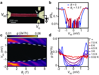
Having obtained the highly ordered epitaxial InAs/Pb heterostructures, we expect hard gap superconductivity with the inherited properties of the Pb filmchang2015hard . To characterise this we performed electron transport measurements on normal metal-superconductor (NS) tunnel junctions with the device geometry shown in Fig. 3a. Prior to normal metal contact deposition, the Pb was selectively etched using H2O, such that a bare InAs segment remained between the normal metal and superconductor (Methods and Supplementary Section 5). This segment acts as a tunnel barrier, tunable using side-gate voltage chang2015hard ; mourik2012signatures . Figure 3b shows differential conductance, , normalised to the normal state conductance, , as a function of source-drain bias voltage at zero magnetic field (red) and finite parallel magnetic field, T (blue). The strong suppression observed for mV reflects the superconducting energy gap, , in the single-particle density of states of the InAs/Pb nanowire. The 100-fold suppression is similar to the hard superconducting gaps reported in III/V nanowires with epitaxial Alchang2015hard ; gazibegovic2017epitaxy ; sestoft2018engineering , polycrystalline SnPendharkarTinArxiv and amorphous TaCarradArXiv191100460Cond-Mat2019 , albeit here with a much larger . Gate voltage-dependent bias spectroscopy (Supplementary Section 4.1) shows that the gap is highly robust in , excluding the possibility that the features attributed to in Fig. 3 are due to e.g. Coulomb blockade.
The evolution of the superconducting gap in a parallel magnetic field, , is shown in Fig. 3c. The gap remains hard over the entire 8.5 T range accessible in our cryostat, highlighted by the blue trace in Fig. 3b. The above-gap resonances likely arise from device-specific states in the tunnel barrier. Figure 3d shows the temperature-dependence of the superconducting gap. As temperature, , is increased, decreases and the edges broaden, up to the critical temperature K. Notably, the gap remains hard at K, and is still prominent at K. The values for , and of the hybrid InAs/Pb nanowires are each more than four times larger than for state-of-the-art Al-based hybrid deviceschang2015hard ; CarradArXiv191100460Cond-Mat2019 ; sestoft2018engineering ; gazibegovic2017epitaxy ; ZhangNature18 , and exceed the metrics reported for InSb/Sn hybridsPendharkarTinArxiv . The dramatic increase in parameter space in terms of , and opens the possibility of performing semiconductor-superconductor hybrid measurements at kelvin temperatures and in entirely new transport regimesAmetScience2016 .
Coulomb blockade spectroscopy of InAs/Pb islands
Essential requirements for semiconductor-superconductor heterostructures in the context of topological qubit development are for isolated hybrid segments – ‘islands’ – to host quantised charge in units of , and the observation of single electron transport through bound states in finite albrecht2016exponential ; shen2018parity ; Vaitiekenasfullshell18 ; PendharkarTinArxiv ; sestoft2018engineering ; vanHeckPRBmodel ; AasenPRX16 ; shen2018parity . Figure 4a shows an InAs/Pb island device, with the Pb selectively removed at either end and contacted by Ti/Au. The side gates control the island-contact coupling and the middle gate adds charge in discrete units. Spectroscopic operation is demonstrated in Fig. 4b, with plotted versus and , revealing periodic Coulomb diamonds due to the sequential addition of charge in units of with an addition energy of meV, which corresponds to shen2018parity . The regions of negative differential conductance below indicate the onset of long-lifetime quasiparticle tunnelingalbrecht2016exponential ; shen2018parity ; Vaitiekenasfullshell18 . For mV, the Coulomb diamond periodicity doubles in , since above-gap quasiparticle states support -periodic transport.
The 2-periodicity for in hard gap hybrids arises due to the odd charge states being lifted in energy by compared to even charge states (Fig. 4c, top panel inset). For soft gap hybridsTakeiPRL2013 ; LeePRLsoftgap the finite density of states within the gap may enable single electron tunneling and -periodicity at zero bias. The importance is that proposed topological qubit architectures rely on magnetic field induced zero energy bound statesAasenPRX16 , and the topologically-protected qubit operation potentially offered by these devices is obviated if soft-gap states are present. Therefore, observing both zero-field -periodic transport and bound-state-induced -periodic transport are highly important steps in hybrid material development.
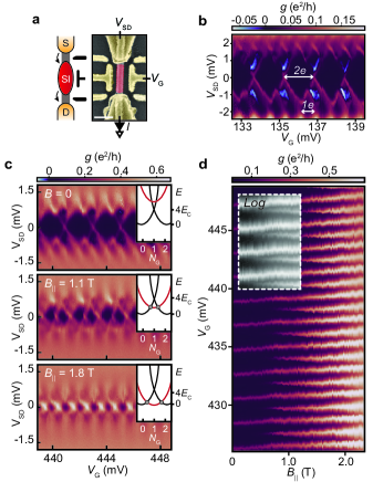
The magnetic field dependent behaviour of our InAs/Pb island was studied using a gate voltage configuration giving a smaller addition energy of meV (Fig. 4c). At (top panel), -periodic charging is observed below . Increased T (Fig. 4c middle panel) causes a bound state to move towards zero energydeng2016majorana ; albrecht2016exponential ; shen2018parity ; Vaitiekenasfullshell18 , and fall below . Odd-state occupation is now enabled (Fig. 4c middle panel inset), with the differing even/odd charging energies producing parity-dependent, even/odd spacing of Coulomb diamonds. Further increasing T (lower panel) brings the bound state close to zero energy.
Figure 4d presents the -dependence of versus at zero bias, corresponding to the data in Fig. 4c. The -periodic peaks split with increasing — highlighted in the inset by the logarithmic greyscale plot — with varying even/odd spacing (see Supplementary Fig. 13). The peak intensity asymmetry between even and odd peaks can be attributed to a difference in the electron-like and hole-like components of the bound states hansen2018probing ; shen2018parity ; PendharkarTinArxiv . These data indicate the emergence of a zero energy hybrid bound state in the InAs/Pb island, consistent with the charging model presented in the insets of Fig. 4c, and previous experiments using Al- and Sn-based hybridsalbrecht2016exponential ; Vaitiekenasfullshell18 ; VaitiekenasPRL18sag ; shen2018parity ; CarradArXiv191100460Cond-Mat2019 ; PendharkarTinArxiv . This demonstrates that InAs/Pb hybrids meet the criteria necessary for sustaining topological superconductivity. Future work including e.g. island-length-dependent studiesalbrecht2016exponential ; Vaitiekenasfullshell18 or demonstrations of braidingAasenPRX16 will contribute to increased understanding towards this goal.
Discussion
The formation of a flat, epitaxially matched single crystal along the entire nanowire confirms the expectations from theoretical considerations of thermodynamic driving forces and structural stability of Pb on InAs. The framework used to investigate elemental superconductor growth on semiconductor nanowires can be extended to other metals and semiconductors, providing increased scope for development of metal/semiconductor epitaxy. In addition to the structural perfection, the epitaxial InAs/Pb hybrids provide a large and hard induced superconducting gap, with corresponding high and , offering a greatly extended experimental parameter space compared to current state-of-the-art materials.lutchyn2018majorana ; CarradArXiv191100460Cond-Mat2019 ; GuskinNanoscale17 ; chang2015hard ; gazibegovic2017epitaxy ; ZhangNature18 ; PendharkarTinArxiv
The observation of -periodicity and bound-state-induced -periodic transport in an InAs/Pb island represents an important step in the development of large , high topological qubitsPendharkarTinArxiv . Moreover, implementing Pb in future devices may benefit from the strong intrinsic spin-orbit coupling of this heavy element superconductor, which has been used to induce spin-orbit coupling by proximity in, e.g., grapheneklimovskikh2017spin ; calleja2015spatial and ferromagnetsruby2017exploring ; nadj2014observation . In the regime of stronger spin-orbit interaction one could potentially avoid the negative aspects of the predicted metallisation effect in Al based devicesReegPRB2018 , where the superconductor-semiconductor coupling increases the induced gap, while decreasing the desired spin-orbit interaction. Finally, recent scanning probe experiments on Pb-based topological systemsnadj2014observation ; menard2019isolated can be complemented by exploring the strongly-coupled, two-bandRubyPRL2015 superconducting nature of Pb in novel hybrid devices.
Methods
The InAs nanowires were grown in a two step growth-process in a solid-source molecular beam epitaxy system. The nanowires were catalysed from electron-beam-lithography-defined Au particles and grown via the vapour-liquid-solid method. In the first step, InAs was grown axially for 30 minutes along the (111)B direction using As4 and a substrate thermocouple temperature () of C, resulting in nanowire lengths m. Growth was then interrupted to increase the As cracker temperature from C to C, yielding As2, and the substrate temperature was lowered to () to C over 20 minutes. The second growth step proceeded under these conditions, radially overgrowing the nanowires for 30 minutes.
After nanowire growth, the substrate was transferred to an attached chamber with a precooled stage without breaking ultra high vacuum (pressures Torr). The substrate was mounted on the cold substrate stage for 3 hours before any subsequent metal deposition to ensure a stable temperature () of 120 K. We note that less time on the cold substrate holder is preferred due to the possible unwanted deposition of foreign materials from the system. To enforce in-situ nanowire masking and only two facet depositions, as shown in Figs 2a,c,e, the wafer was aligned relative to the pre-defined nanowire array. Pb was deposited with a shallow angle and rate (3 Ås-1) using electron beam evaporation. After the metal deposition the substrate was kept cold on the substrate holder for more than 10 hours to limit dewetting, and produced films with flatter morphology.
SEM micrographs were produced by combining signals from the surface sensitive secondary electron detector and the atomic weight sensitive backscatter electron detector since Pb forms a flat film which is only seen clearly when using an atomic weight sensitive technique. STEM images were acquired using an FEI Titan 80-300 TEM equipped with a probe Cs corrector and operated at 300 kV. HAADF STEM images were taken with a beam convergence semi angle of mrad. The inner and outer collection semi angle of the HAADF detector was set to 54 and 270 mrad, respectively. Cross section specimens of the nanowires were prepared using an FEI Versa 3D focused ion beam scanning electron microscope (FIB SEM), following Pt deposition to protect the nanowires. A final polish of the TEM specimens in FIB SEM with a 2 kV and 27 pA ion beam was used to minimize the damage caused by the Ga ion beam. The micrograph in Fig. 1d was produced by drift correcting and summing the amplitude of 100 HR HAADF STEM micrographs with a short acquisition time. The STEM micrographs in Figs 1e,f were noise reduced by removing the Fourier spectrum background amplitude. The structural simulation of the hetero-epitaxial interface in Fig. 1 was performed using the software program Vestamomma2011vesta .
Devices (Figs 3 and 4) were fabricated using electron beam lithography and lift off techniques, with Ti/Au (5 nm/250 nm) thin films for contacts and gates. H2O (MilliQ with resistivity M) was used as a selective etchant to remove Pb from the semiconductor surface, and Ar+ milling used prior to contact deposition to remove native InAs oxides. Full details are given in the Supplementary Information. Standard voltage-biased lock-in techniques were used to measure the conductance of the devices in a dilution refrigerator with a base temperature of 25 mK. Prior to collecting the presented data on island devices (Fig. 4), the cross-coupling of the gates was measured. To collect the presented data, the gates were swept simultaneously according to the measured proportionality factors to ensure that only altered island occupation and did not appreciably alter the island-lead coupling, or the chemical potential of the InAs segments.
Acknowledgements
This work was funded by the Danish National Research Foundation, European Union’s Horizon 2020 research and innovation programme under grant agreement No.823717 (ESTEEM3), FETOpen grant no. 828948 (AndQC) and QuantERA project no. 127900 (SuperTOP), Villum Foundation project no. 25310, Innovation Fund Denmark’s Quantum Innovation Center Qubiz, and the Carlsberg Foundation. J.d.B. acknowledges support by the Netherlands Organisation for Scientific Research (NWO/OCW), as part of the Frontiers of Nanoscience program. We thank M. Bjergfelt, A. Geresdi, T.S. Jespersen, J. Paaske, J.C.E. Saldaña and S. Vaitiekenas for useful discussions. C.B. Sørensen is gratefully acknowledged for technical assistance and support.
Competing interests
The authors declare no competing interests
Supplementary Information
Supplementary information containing extended information on metal-on-semiconductor growth, structural characterisation and transport measurements is available at https://sid.erda.dk/sharelink/eeL2CxBB6p.
References
- (1) Lutchyn, R. t. et al. Majorana zero modes in superconductor–semiconductor heterostructures. Nature Reviews Materials 3, 52–68 (2018).
- (2) Krogstrup, P. et al. Epitaxy of semiconductor–superconductor nanowires. Nature Materials 14, 400 (2015).
- (3) Mourik, V. et al. Signatures of Majorana fermions in hybrid superconductor-semiconductor nanowire devices. Science 336, 1003–1007 (2012).
- (4) Das, A. et al. Zero-bias peaks and splitting in an Al-InAs nanowire topological superconductor as a signature of Majorana fermions. Nature Physics 8, 887–895 (2012).
- (5) Deng, M. T. et al. Anomalous Zero-Bias Conductance Peak in a Nb-InSb Nanowire-Nb Hybrid Device. Nano Letters 12, 6414–6419 (2012).
- (6) Deng, M. et al. Majorana bound state in a coupled quantum-dot hybrid-nanowire system. Science 354, 1557–1562 (2016).
- (7) Zhang, H. et al. Quantized Majorana conductance. Nature 556, 74–79 (2018).
- (8) Pendharkar, M. et al. Parity-preserving and magnetic field resilient superconductivity in indium antimonide nanowires with tin shells. Preprint at http://arxiv.org/abs/1912.06071 (2019).
- (9) Klinovaja, J. & Loss, D. Time-reversal invariant parafermions in interacting Rashba nanowires. Phys. Rev. B 90, 045118 (2014).
- (10) Larsen, T. W. et al. Semiconductor-Nanowire-Based Superconducting Qubit. Physical Review Letters 115, 127001 (2015).
- (11) Luthi, F. et al. Evolution of Nanowire Transmon Qubits and Their Coherence in a Magnetic Field. Physical Review Letters 120, 100502 (2018).
- (12) Tosi, L. et al. Spin-Orbit Splitting of Andreev States Revealed by Microwave Spectroscopy. Phys. Rev. X 9, 011010 (2019).
- (13) Hays, M. et al. Direct Microwave Measurement of Andreev-Bound-State Dynamics in a Semiconductor-Nanowire Josephson Junction. Phys. Rev. Lett. 121, 047001 (2018).
- (14) Prada, E. et al. From Andreev to Majorana bound states in hybrid superconductor-semiconductor nanowires. Preprint at http://arxiv.org/abs/1911.04512 (2019).
- (15) Chang, W. et al. Hard gap in epitaxial semiconductor–superconductor nanowires. Nature Nanotechnology 10, 232 (2015).
- (16) Oreg, Y., Refael, G. & von Oppen, F. Helical Liquids and Majorana Bound States in Quantum Wires. Physical Review Letters 105, 177002 (2010).
- (17) Lutchyn, R. M., Sau, J. D. & Das Sarma, S. Majorana Fermions and a Topological Phase Transition in Semiconductor-Superconductor Heterostructures. Physical Review Letters 105, 077001 (2010).
- (18) Albrecht, S. M. et al. Exponential protection of zero modes in Majorana islands. Nature 531, 206 (2016).
- (19) Carrad, D. J. et al. Shadow Lithography for In-Situ Growth of Generic Semiconductor/Superconductor Devices. Preprint at http://arxiv.org/abs/1911.00460 (2019).
- (20) Bjergfelt, M. et al. Superconducting vanadium/indium-arsenide hybrid nanowires. Nanotechnology 30, 294005 (2019).
- (21) Shen, J. et al. Parity transitions in the superconducting ground state of hybrid InSb-Al Coulomb islands. Nature Communications 9, 4801 (2018).
- (22) Vaitiekėnas, S., Deng, M.-T., Krogstrup, P. & Marcus, C. M. Flux-induced Majorana modes in full-shell nanowires. Preprint at http://arxiv.org/abs/1809.05513 (2018).
- (23) Aasen, D. et al. Milestones Toward Majorana-Based Quantum Computing. Physical Review X 6, 031016 (2016).
- (24) Güsken, N. A. et al. MBE growth of Al/InAs and Nb/InAs superconducting hybrid nanowire structures. Nanoscale 9, 16735–16741 (2017).
- (25) Sestoft, J. E. et al. Engineering hybrid epitaxial InAsSb/Al nanowires for stronger topological protection. Physical Review Materials 2, 044202 (2018).
- (26) Vaitiekėnas, S. et al. Selective-Area-Grown Semiconductor-Superconductor Hybrids: A Basis for Topological Networks. Physical Review Letters 121, 147701 (2018).
- (27) Aseev, P. et al. Selectivity Map for Molecular Beam Epitaxy of Advanced III–V Quantum Nanowire Networks. Nano Letters 19, 218–227 (2019).
- (28) Kjaergaard, M. et al. Quantized conductance doubling and hard gap in a two-dimensional semiconductor–superconductor heterostructure. Nature Communications 7, 12841 (2016).
- (29) Shabani, J. et al. Two-dimensional epitaxial superconductor-semiconductor heterostructures: A platform for topological superconducting networks. Phys. Rev. B 93, 155402 (2016).
- (30) Sau, J. D. & Sarma, S. D. Realizing a robust practical Majorana chain in a quantum-dot-superconductor linear array. Nature Communications 3, 964 (2012).
- (31) Su, Z. et al. Andreev molecules in semiconductor nanowire double quantum dots. Nature Communications 8, 1–6 (2017).
- (32) Krizek, F. et al. Growth of InAs wurtzite nanocrosses from hexagonal and cubic basis. Nano Letters 17, 6090–6096 (2017).
- (33) Gazibegovic, S. et al. Epitaxy of advanced nanowire quantum devices. Nature 548, 434 (2017).
- (34) Pentcheva, R. et al. Non-Arrhenius behavior of the island density in metal heteroepitaxy: Co on Cu (001). Physical Review Letters 90, 076101 (2003).
- (35) Venables, J. & Spiller, G. Nucleation and growth of thin films. In Surface Mobilities on Solid Materials, 341–404 (Springer, 1983).
- (36) Vesselinov, M. I. Crystal growth for beginners: Fundamentals of nucleation, crystal growth and epitaxy (World Scientific, 2016).
- (37) Thompson, C. V. Solid-state dewetting of thin films. Annual Review of Materials Research 42, 399–434 (2012).
- (38) Amet, F. et al. Supercurrent in the quantum Hall regime. Science 352, 966–969 (2016).
- (39) van Heck, B., Lutchyn, R. M. & Glazman, L. I. Conductance of a proximitized nanowire in the Coulomb blockade regime. Phys. Rev. B 93, 235431 (2016).
- (40) Takei, S., Fregoso, B. M., Hui, H.-Y., Lobos, A. M. & Das Sarma, S. Soft Superconducting Gap in Semiconductor Majorana Nanowires. Phys. Rev. Lett. 110, 186803 (2013).
- (41) Lee, E. J. H. et al. Zero-bias anomaly in a nanowire quantum dot coupled to superconductors. Phys. Rev. Lett. 109, 186802 (2012).
- (42) Hansen, E. B., Danon, J. & Flensberg, K. Probing electron-hole components of subgap states in Coulomb blockaded Majorana islands. Physical Review B 97, 041411 (2018).
- (43) Klimovskikh, I. I. et al. Spin–orbit coupling induced gap in graphene on Pt (111) with intercalated Pb monolayer. ACS Nano 11, 368–374 (2017).
- (44) Calleja, F. et al. Spatial variation of a giant spin–orbit effect induces electron confinement in graphene on Pb islands. Nature Physics 11, 43 (2015).
- (45) Ruby, M., Heinrich, B. W., Peng, Y., von Oppen, F. & Franke, K. J. Exploring a proximity-coupled Co chain on Pb (110) as a possible majorana platform. Nano Letters 17, 4473–4477 (2017).
- (46) Nadj-Perge, S. et al. Observation of Majorana fermions in ferromagnetic atomic chains on a superconductor. Science 346, 602–607 (2014).
- (47) Reeg, C., Loss, D. & Klinovaja, J. Metallization of a Rashba wire by a superconducting layer in the strong-proximity regime. Phys. Rev. B 97, 165425 (2018).
- (48) Ménard, G. C. et al. Isolated pairs of Majorana zero modes in a disordered superconducting lead monolayer. Nature Communications 10, 2587 (2019).
- (49) Ruby, M., Heinrich, B. W., Pascual, J. I. & Franke, K. J. Experimental Demonstration of a Two-Band Superconducting State for Lead Using Scanning Tunneling Spectroscopy. Phys. Rev. Lett. 114, 157001 (2015).
- (50) Momma, K. & Izumi, F. VESTA 3 for three-dimensional visualization of crystal, volumetric and morphology data. Journal of Applied Crystallography 44, 1272–1276 (2011).