Inelastic electron tunneling in 2H-TaxNb1-xSe2 evidenced by scanning tunneling spectroscopy
Abstract
We report a detailed study of tunneling spectra measured on 2H-TaxNb1-xSe2 () single crystals using a low-temperature scanning tunneling microscope. The prominent gap-like feature unintelligible for a long time was found to be accompanied by some “in-gap” fine structures. By investigating the second-derivative spectra and their temperature and magnetic field dependencies, we were able to prove that inelastic electron tunneling is the origin of these features and obtain the Eliashberg function of 2H-TaxNb1-xSe2 at atomic scale, providing a potential way to study the local Eliashberg function and phonon spectra of the related transition-metal dichalcogenides.
As a prototype of transition-metal dichalcogenides (TMDs), 2H-NbSe2 keeps attracting great interest since it provides a platform, both in bulk and in its two-dimensional form, to study the mechanism of charge-density waves (CDWs) Wilson et al. (1975); Grüner (1988); Ugeda et al. (2016), interplay between CDWs and superconductivity (SC) Kiss et al. (2007); Chatterjee et al. (2015); Cho et al. (2018), potential applications in electronic devices Efetov et al. (2015); Yabuki et al. (2016); Kim et al. (2017), and so on. In recent years, there is growing consensus that it is the wave-vector-dependent strong electron-phonon coupling (EPC) that drives CDW formation Weber et al. (2011); Flicker and van Wezel (2015); Rossnagel (2011). However, unlike the typical strong EPC system of Pb Rowell et al. (1969), no characteristics of the tunneling spectra of 2H-NbSe2 have been identified as its EPC function, i.e., the Eliashberg function. The dominant low-energy feature other than the superconducting gap is the kinks at approximately 35 mV, which has been observed repeatedly by scanning tunneling microscopy/spectroscopy (STM/STS) Hess et al. (1991); Soumyanarayanan et al. (2013). This well-known gap-like feature was initially regarded as the CDW gap Hess et al. (1991), but has not been demonstrated by subsequent measurements of angle-resolved photoelectron spectroscopy (ARPES) Valla et al. (2004); Borisenko et al. (2009). A recent STM/STS experiment ascribed it to the combination of a 35-mV electron self-energy effect and a non-symmetric CDW gap of approximately 12 meV Soumyanarayanan et al. (2013), which is supported by the later ARPES experiment Chatterjee et al. (2015). Nonetheless, it is confusing to note that no other phonon modes have been noticed by STS, although various modes in addition to the 35-meV one can be observed in the energy-momentum dispersions from ARPES Rahn et al. (2012).
In this work, we performed precise STM/STS measurements for 2H-TaxNb1-xSe2 single crystals. In addition to the 35-mV gap-like feature, a series of “in-gap” shoulders/steps were observed in all samples. By investigating the second-derivative spectra of and its temperature and magnetic field evolutions, we demonstrated that these spectroscopic features, including the long-term incomprehensible 35-mV enigma, originate from the inelastic electron tunneling process instead of a CDW gap Hess et al. (1991) or the electron self-energy effect Soumyanarayanan et al. (2013). Meanwhile, a double Fermi-Dirac broadening effect was found to be a convenient way to distinguish an inelastic electron tunneling process. Then, the real-space resolved Eliashberg functions were obtained from inelastic electron tunneling spectroscopy (IETS), which might be extended to the study of other members of the TMD family.
The 2H-TaxNb1-xSe2 single crystals studied here were grown with the iodine vapor transport method Dalrymple et al. (1986). The spatially resolved tunneling experiments were carried out on a home-built low-temperature scanning tunneling microscope, in which a single-crystalline sample was cold-cleaved in situ and then inserted into the STM head immediately. Electrochemically etched tungsten tips were used for the STM/STS measurements after field-emission treatment on a piece of gold. The tunneling spectra of were obtained using a standard lock-in technique with a frequency of 373.1 Hz and a modulation amplitude of 0.1 or 0.2 mV SI .
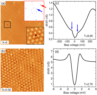
2H-NbSe2 shows a CDW transition at 33 K and a superconducting transition of 7.1 K Moncton et al. (1975, 1977). Figure 1(a) shows a topographic image of 2H-NbSe2, in which the atomic resolution is demonstrated by the single vacancy of an Se atom enclosed in the black box. CDW order can be clearly seen as the bright spots almost every three atoms along the sixfold- symmetric axes, and the corresponding wave vector is indicated in the inset. It is known that a moderate Ta doping into Nb sites in pristine 2H-NbSe2 will impair CDW order, whereas it does not seriously change the electronic structures Renner et al. (1991). As demonstrated in Fig. 1(b), the long range CDW is broken into domains with nanometer scales, in some of which CDW has been strongly suppressed. Figure 1(c) gives a large-bias range tunneling spectrum of 2H-NbSe2, where a prominent gap-like feature shows up between the inflection points at approximately 35 mV. At low temperatures below , a superconducting gap (1.1meV) develops as presented in Fig. 1(d). The 35-meV gap-like feature has long been regarded as the CDW gap Hess et al. (1991), while its equivalent in ARPES data has never been found Valla et al. (2004); Borisenko et al. (2009); Rahn et al. (2012).
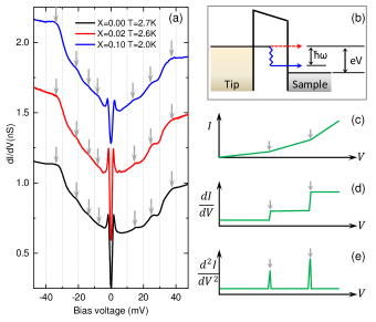
To examine the possible influence of CDWs on the tunneling spectrum, we have studied a series of 2H-TaxNb1-xSe2 () single crystals. As shown in Fig. 2(a), both the superconducting gap and the 35-mV “gap” are very clear for all the samples. Remarkably, distinct fine structures were found inside the big “gap” showing themselves as a series of shoulders or steps (including the 35-meV one) marked by the arrows. This is reminiscent of the inelastic electron tunneling process, the schematic of which is given in Fig. 2(b). In brief, when the energy of tunneling electrons reaches that of a vibrational mode in a EPC system, they could lose their energies to excite the phonon mode and open an inelastic tunneling channel You et al. (2017). However, due to Fermi’s golden rule, such inelastic channel is forbidden if the tunneling electron’s energy is below the quantized phonon energy. In experiments, the opening of additional inelastic channels will cause slope changes of a curve, sharp shoulders/steps in the tunneling conductance of , and corresponding peaks at each phonon energy in , as depicted in Figs. 2(c)-(e). Actually, versus directly reflects the effective EPC spectrum , i.e., the Eliashberg function Taylor (1992); Schackert et al. (2015). Here, is the phonon density of states (DOS) and the energy-dependent EPC strength. This method, known as IETS, could be utilized to reveal the vibrational spectra of molecules at the interface of a tunneling junction Stipe et al. (1998); Ho (2002); Galperin et al. (2007); You et al. (2017) or, in a few cases, to obtain the collective vibrations or Eliashberg functions in solids Vitali et al. (2004); Gawronski et al. (2008); Altfeder et al. (2012); Schackert et al. (2015); Jandke et al. (2016).
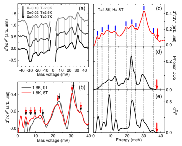
Except for the non-symmetric background of the electron DOS and superconducting gap, all the spectral features shown in Fig. 2(a) look qualitatively similar to that of Fig. 2(d). Figure 3(a) displays the spectra derived from the data in Fig. 2(a), showing similar shapes for all the doping levels and excluding the CDW order as the major origin of the observed fine spectral structures and the enigmatic 35-mV “gap”. In contrast, the Eliashberg function was expected to be not obviously dependent on the Ta doping up to a content of 10% according to our first-principles calculations SI . Furthermore, as shown in Fig. 3(b), when superconductivity is suppressed by a magnetic field and hence the superconducting gap is closed, some peaks shift slightly towards lower energies while some others do not. This is in good agreement with the momentum-dependent EPC and superconducting gap in 2H-NbSe2 Valla et al. (2004); Rahn et al. (2012). In the framework of IETS, a peak related to a specific phonon in the normal state will shift to in the superconducting state. Thus, the IETS peaks coupled to different parts of the Fermi surfaces will shift to different energy scales determined by the momentum dependence of . As shown in Figs. 3(c)-(e), both the phonon DOS and Eliashberg function of 2H-NbSe2 were calculated SI in comparison with the experimental data. Almost all the characteristic peaks marked in Fig. 3(c) have their counterparts in the calculated phonon DOS or as given in Figs. 3(d) and (e). Furthermore, the upper boundary of the phonon DOS or at approximately 37 meV is very close to the value of 38 meV in , as denoted by the arrows.

The identification of the Eliashberg function here elucidates the mechanism of the 35-mV enigma as an inelastic electron tunneling process. This provides a good opportunity to acquire knowledge of the IETS in a superconducting system. To this end, we have measured the temperature and magnetic field dependencies of IETS. As exemplified by Fig. 4(a), the peaks in decay gradually with increasing temperature, but survive well above . In the normal state at = 8 K, the data of zero field look the same as that of a 8-T field, ruling out any form of magnetic effect on EPC. In Fig. 4(b), the spectral weights integrated between 10 meV (selected to exclude the influence of superconducting gap at lower bias) and 45 meV are plotted against temperature for both zero field and 8 T. No obvious temperature dependence can be seen, indicating a nearly constant Eliashberg function in the studied temperature range. Thus, the observed peak decaying with temperature should originate from the thermal broadening effect. To confirm this judgement, we present in Fig. 4(c) the temperature dependence of the peak intensity defined as the drop between the highest peak and the dip beside it as shown in Fig. 4(a). It was found that the peak intensity enhances continuously with decreasing temperature and an extra enhancement occurs in the superconducting state compared with the normal state.
We have tried to build a simple model to quantitatively explain the normal-state data, in which inelastic tunneling is considered as a two-step process and the attenuation of peak intensity is due to Fermi-Dirac (thermal) broadening. For an ordinary tunneling process at a finite temperature, the thermal broadening of the tunneling spectrum is rooted in the Fermi-Dirac distributions of the occupied electron DOS at both banks of the tunneling junction. If the electron DOS stays the same in the studied temperature range, the broadening effect is equivalent to a convolution of the zero-temperature spectrum with a temperature-dependent Fermi-Dirac broadening function as illustrated in the inset of Fig. 4(c). In contrast, inelastic tunneling includes two steps, i.e., the ordinary tunneling and a subsequent transition to a lower energy by exciting a phonon. Since the Fermi-Dirac broadening effect takes effect in the second process as well, a double Fermi-Dirac broadening should be considered in our calculations SI . The good agreement between this simple model [see the solid line in Fig. 4(c)] and experimental data further support that the fine spectral structures of 2H-TaxNb1-xSe2 are indeed related to the inelastic electron tunneling process. The line calculated with single Fermi-Dirac broadening is also presented, significantly deviating from the experimental data. Therefore, the constructed model provides a convenient way to distinguish IETS from other mechanisms, such as the self-energy effect in which single Fermi-Dirac broadening is involved.
According to the IETS mechanism, it is easy to understand the above-mentioned additional enhancement of peak intensity in the superconducting state. The peak intensity at a particular phonon energy is determined by the phonon DOS at this energy and the electron DOS first involved in the inelastic channel. Since quasiparticle DOS peaks (coherence peaks) develop at the gap edges below , the IETS peak will become stronger accordingly, in comparison with the normal state. With decreasing temperature, the coherence peaks are intensified continuously, resulting in an increasingly more prominent IETS peak. Therefore, our experiments indicate that such electron DOS redistribution can be used to enhance spectral intensity and discern the Eliashberg function more easily.
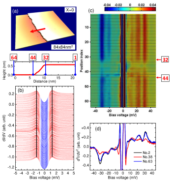
Using STM/STS offers the possibility to measure IETS at the atomic scale. However, for the moment, this methodology has been limited to a few solid materials, such as graphite/graphene Vitali et al. (2004); Zhang et al. (2008); Cervenka et al. (2010); Natterer et al. (2015), copper Gawronski et al. (2008); Minamitani et al. (2016), gold Gawronski et al. (2008), and the only superconducting material of lead Altfeder et al. (2012); Schackert et al. (2015); Jandke et al. (2016). The observation in this work extends the field of research to the widely concerned TMDs, an easily tailored system suitable to further study or manipulate EPC. For example, we could examine the influence of a structural defect on the Eliashberg function and superconductivity of 2H-NbSe2 simultaneously. Figure 5(b) shows a series of spectra taken sequentially at 64 points along a line across a half-unit-cell step displayed in Fig. 5(a). The superconducting gap remains almost constant along the trajectory, whereas the spectrum of Fig. 5(c) shows a remarkable change in the step region of points 32-44. As presented in Fig. 5(d), the spectral weight at the step is seriously suppressed above 15 mV compared with those two spectra taken near the opposite ends of the trace, which should be related to the abrupt changes of either electron/phonon DOS or EPC. Therefore, the spatially resolved spectra given in Fig. 5 clearly demonstrate the immunity of the bulk Bardeen-Cooper-Schrieffer superconductivity to a local variation of the Eliashberg function. The situation is expected to be different in a size-limited system (say, a few-layered one) and thus deserves more attention in the future..
In summary, tunneling spectra of 2H-TaxNb1-xSe2 single crystals have been measured at low temperatures and high magnetic fields. Using first-principles calculations and a simple two-step tunneling model, we were able to relate the derived spectra of to the inelastic electron tunneling process and hence the Eliashberg functions. These results not only resolve the long-standing enigma of the 35-mV “gap”-like feature observed in 2H-NbSe2, but also pave a way to explore the spatially dependent electron-phonon coupling in the widely concerned transition-metal dichalcogenides.
Acknowledgements.
We thank T. Xiang, C. Ren, and K. Jin for fruitful discussions. This work was financially supported by the National Key R&D Program of China (Grant No. 2017YFA0403502, 2017YFA0302904, 2018YFA0305602, 2017YFA0303201), National Natural Science Foundation of China (Grant No. 11574372, 11322432, 11804379, 11674331), “100 Talents Project” of the Chinese Academy of Sciences, CASHIPS Director’s Fund (Grant No. BJPY2019B03), Youth Innovation Promotion Association of CAS (Grant No. 2017483), and The Recruitment Program for Leading Talent Team of Anhui Province (2019-16). A portion of this work was supported by the High Magnetic Field Laboratory of Anhui Province.References
- Wilson et al. (1975) J. Wilson, F. D. Salvo, and S. Mahajan, Advances in Physics 24, 117 (1975).
- Grüner (1988) G. Grüner, Rev. Mod. Phys. 60, 1129 (1988).
- Ugeda et al. (2016) M. M. Ugeda, A. J. Bradley, Y. Zhang, S. Onishi, Y. Chen, W. Ruan, C. Ojeda-Aristizabal, H. Ryu, M. T. Edmonds, H.-Z. Tsai, et al., Nature Physics 12, 92 (2016).
- Kiss et al. (2007) T. Kiss, T. Yokoya, A. Chainani, S. Shin, T. Hanaguri, M. Nohara, and H. Takagi, Nature Physics 3, 720 (2007).
- Chatterjee et al. (2015) U. Chatterjee, J. Zhao, M. Iavarone, R. Di Capua, J. P. Castellan, G. Karapetrov, C. D. Malliakas, M. G. Kanatzidis, H. Claus, J. P. C. Ruff, et al., Nature Communications 6, 6313 (2015).
- Cho et al. (2018) K. Cho, M. Konczykowski, S. Teknowijoyo, M. A. Tanatar, J. Guss, P. B. Gartin, J. M. Wilde, A. Kreyssig, R. J. McQueeney, A. I. Goldman, et al., Nature Communications 9, 2796 (2018).
- Efetov et al. (2015) D. K. Efetov, L. Wang, C. Handschin, K. B. Efetov, J. Shuang, R. Cava, T. Taniguchi, K. Watanabe, J. Hone, C. R. Dean, et al., Nature Physics 12, 328 (2015).
- Yabuki et al. (2016) N. Yabuki, R. Moriya, M. Arai, Y. Sata, S. Morikawa, S. Masubuchi, and T. Machida, Nature Communications 7, 10616 (2016).
- Kim et al. (2017) M. Kim, G.-H. Park, J. Lee, J. H. Lee, J. Park, H. Lee, G.-H. Lee, and H.-J. Lee, Nano Letters 17, 6125 (2017).
- Weber et al. (2011) F. Weber, S. Rosenkranz, J.-P. Castellan, R. Osborn, R. Hott, R. Heid, K.-P. Bohnen, T. Egami, A. H. Said, and D. Reznik, Phys. Rev. Lett. 107, 107403 (2011).
- Flicker and van Wezel (2015) F. Flicker and J. van Wezel, Nature Communications 6, 7034 (2015).
- Rossnagel (2011) K. Rossnagel, Journal of Physics: Condensed Matter 23, 213001 (2011).
- Rowell et al. (1969) J. M. Rowell, W. L. McMillan, and W. L. Feldmann, Phys. Rev. 178, 897 (1969).
- Hess et al. (1991) H. Hess, R. Robinson, and J. Waszczak, Physica B: Condensed Matter 169, 422 (1991).
- Soumyanarayanan et al. (2013) A. Soumyanarayanan, M. M. Yee, Y. He, J. van Wezel, D. J. Rahn, K. Rossnagel, E. W. Hudson, M. R. Norman, and J. E. Hoffman, Proceedings of the National Academy of Sciences 110, 1623 (2013).
- Valla et al. (2004) T. Valla, A. V. Fedorov, P. D. Johnson, P.-A. Glans, C. McGuinness, K. E. Smith, E. Y. Andrei, and H. Berger, Phys. Rev. Lett. 92, 086401 (2004).
- Borisenko et al. (2009) S. V. Borisenko, A. A. Kordyuk, V. B. Zabolotnyy, D. S. Inosov, D. Evtushinsky, B. Büchner, A. N. Yaresko, A. Varykhalov, R. Follath, W. Eberhardt, et al., Phys. Rev. Lett. 102, 166402 (2009).
- Rahn et al. (2012) D. J. Rahn, S. Hellmann, M. Kalläne, C. Sohrt, T. K. Kim, L. Kipp, and K. Rossnagel, Phys. Rev. B 85, 224532 (2012).
- Dalrymple et al. (1986) B. Dalrymple, S. Mroczkowski, and D. Prober, Journal of Crystal Growth 74, 575 (1986).
- (20) See Supplemental Material for details of the STM/STS experiments, the phonon DOS calculations which includes Refs. [38-46] and modulation of tunneling conductivity from electron-phonon coupling.
- Moncton et al. (1975) D. E. Moncton, J. D. Axe, and F. J. DiSalvo, Phys. Rev. Lett. 34, 734 (1975).
- Moncton et al. (1977) D. E. Moncton, J. D. Axe, and F. J. DiSalvo, Phys. Rev. B 16, 801 (1977).
- Renner et al. (1991) C. Renner, A. D. Kent, P. Niedermann, O. Fischer, and F. Lévy, Phys. Rev. Lett. 67, 1650 (1991).
- You et al. (2017) S. You, J.-T. L , J. Guo, and Y. Jiang, Advances in Physics: X 2, 907 (2017).
- Taylor (1992) M. Taylor, Ultramicroscopy 42, 215 (1992).
- Schackert et al. (2015) M. Schackert, T. Märkl, J. Jandke, M. Hölzer, S. Ostanin, E. K. U. Gross, A. Ernst, and W. Wulfhekel, Phys. Rev. Lett. 114, 047002 (2015).
- Stipe et al. (1998) B. C. Stipe, M. A. Rezaei, and W. Ho, Science 280, 1732 (1998).
- Ho (2002) W. Ho, The Journal of Chemical Physics 117, 11033 (2002).
- Galperin et al. (2007) M. Galperin, M. A. Ratner, and A. Nitzan, Journal of Physics: Condensed Matter 19, 103201 (2007).
- Vitali et al. (2004) L. Vitali, M. A. Schneider, K. Kern, L. Wirtz, and A. Rubio, Phys. Rev. B 69, 121414(R) (2004).
- Gawronski et al. (2008) H. Gawronski, M. Mehlhorn, and K. Morgenstern, Science 319, 930 (2008).
- Altfeder et al. (2012) I. Altfeder, K. A. Matveev, and A. A. Voevodin, Phys. Rev. Lett. 109, 166402 (2012).
- Jandke et al. (2016) J. Jandke, P. Hlobil, M. Schackert, W. Wulfhekel, and J. Schmalian, Phys. Rev. B 93, 060505(R) (2016).
- Zhang et al. (2008) Y. Zhang, V. W. Brar, F. Wang, C. Girit, Y. Yayon, M. Panlasigui, A. Zettl, and M. F. Crommie, Nature Physics 4, 627 (2008).
- Cervenka et al. (2010) J. Cervenka, K. van de Ruit, and C. F. J. Flipse, physica status solidi (b) 247, 2992 (2010).
- Natterer et al. (2015) F. D. Natterer, Y. Zhao, J. Wyrick, Y.-H. Chan, W.-Y. Ruan, M.-Y. Chou, K. Watanabe, T. Taniguchi, N. B. Zhitenev, and J. A. Stroscio, Phys. Rev. Lett. 114, 245502 (2015).
- Minamitani et al. (2016) E. Minamitani, R. Arafune, N. Tsukahara, Y. Ohda, S. Watanabe, M. Kawai, H. Ueba, and N. Takagi, Phys. Rev. B 93, 085411 (2016).
- Giannozzi et al. (2009) P. Giannozzi, S. Baroni, N. Bonini, M. Calandra, R. Car, C. Cavazzoni, D. Ceresoli, G. L. Chiarotti, M. Cococcioni, I. Dabo, et al., J. Phys. Condens. Matter 21, 395502 (2009).
- Hohenberg and Kohn (1964) P. Hohenberg and W. Kohn, Phys. Rev. 136, B864 (1964).
- Kohn and Sham (1965) W. Kohn and L. J. Sham, Phys. Rev. 140, A1133 (1965).
- Baroni et al. (2001) S. Baroni, S. De Gironcoli, A. Dal Corso, and P. Giannozzi, Rev. Mod. Phys. 73, 515 (2001).
- Perdew et al. (1996) J. P. Perdew, K. Burke, and M. Ernzerhof, Phys. Rev. Lett. 77, 3865 (1996).
- Blöchl (1994) P. E. Blöchl, Phys. Rev. B 50, 17953 (1994).
- Kresse and Joubert (1999) G. Kresse and D. Joubert, Phys. Rev. B 59, 1758 (1999).
- Thonhauser et al. (2015) T. Thonhauser, S. Zuluaga, C. A. Arter, K. Berland, E. Schröder, and P. Hyldgaard, Phys. Rev. Lett. 115, 136402 (2015).
- Thonhauser et al. (2007) T. Thonhauser, V. R. Cooper, S. Li, A. Puzder, P. Hyldgaard, and D. C. Langreth, Phys. Rev. B 76, 125112 (2007).