Demonstration of a Thermally-Coupled Row-Column SNSPD Imaging Array
Abstract
While single-pixel superconducting nanowire single photon detectors (SNSPDs) have demonstrated remarkable efficiency and timing performance from the UV to near-IR, scaling these devices to large imaging arrays remains challenging. Here, we propose a new SNSPD multiplexing system using thermal coupling and detection correlations between two photosensitive layers of an array. Using this architecture with the channels of one layer oriented in rows and the second layer in columns, we demonstrate imaging capability in 16-pixel arrays with accurate spot tracking at the few photon level. We also explore the performance tradeoffs of orienting the top layer nanowires parallel and perpendicular to the bottom layer. The thermally-coupled row-column scheme is readily able to scale to the kilopixel size with existing readout systems, and when combined with other multiplexing architectures, has the potential to enable megapixel scale SNSPD imaging arrays.
keywords:
single-photon detector, nanowires, SNSPD, superconducting devices, detector arraysJet Propulsion Laboratory, California Institute of Technology, Pasadena, CA, United States. This document is the unedited Author’s version of a Submitted Work that was subsequently accepted for publication in Nano Letters, copyright ©American Chemical Society after peer review. To access the final edited and published work see http://dx.doi.org/10.1021/acs.nanolett.0c00246.
©2020. California Institute of Technology. Government sponsorship acknowledged.
Single-pixel superconducting nanowire single photon detectors (SNSPDs) 1 have achieved remarkable performance including 90% detection efficiency 2, 3, timing jitter below at telecom wavelengths 4, 5, 6, and dark count rates below 0.5 counts per hour 7, 8. Emerging applications such as focal plane arrays for MIR astronomical spectroscopy 9, detectors for dark matter search efforts 8, telecom LIDAR10, and quantum imaging would benefit from SNSPDs’ high efficiency and low intrinsic dark count rate performance for low photon-flux signals over wide wavelength ranges. However, these applications also require kilopixel to megapixel arrays covering millimeter-scale active areas. Traditional SNSPD readout uses high bandwidth RF cables for each channel of an array, but this places an unsustainable heat load on the cryogenic stage as the number of cables scales beyond a few tens of lines. Arrays of 64 pixels have been demonstrated using direct readout 11 but scaling to the kilopixel range is challenging. To overcome this limitation, various multiplexing schemes have been demonstrated which enable imaging capability while reducing the number of RF cables. One approach uses a row-column biasing scheme 12, 13, 14 and correlations between the detections on row and column readout channels to determine which pixel registered a detection. This architecture is able to read an array with readout lines. However, this architecture suffers from current redistribution among the pixels of each bias line, limiting the maximum count rate and degrading the timing jitter 13. Multiplexing based on SFQ readout has been demonstrated in both standard 15 and row-column 14 arrays, but this approach still struggles with the heat load placed on the cryogenic stage. A third approach fashions the active nanowire element as a delay line and uses differential readout to infer the location of absorption along the length of the nanowire 16, 17. This design requires the use of large impedance matching tapers to improve signal quality 18, but this adds significant kinetic inductance to the device which reduces the maximum count rate (MCR). Furthermore, the spatial resolution is ultimately limited by the timing jitter of the system, necessitating the use of high performance amplifiers and readout electronics. As an alternative, the microwave kinetic inductance detector (MKID) community has used frequency multiplexing to develop detector arrays with several to tens of kilopixels using few microwave feedlines at the cryogenics stage 19, 20, 21. While this type of frequency multiplexing has been demonstrated in SNSPD arrays using both DC 22 and AC 23 nanowire biasing, significant challenges remain in successfully scaling these architectures to the kilopixel scale.
We propose and demonstrate a new method of multiplexing, the thermally-coupled row-column (thermal row-column or TRC), which uses thermal coupling between two active SNSPD layers with channels arranged in rows and columns. By measuring coincidence events between row and column channels, the location of absorption is inferred to be the intersection of those channels, forming a pixel. The channels are electrically isolated at low frequencies, so there is no current redistribution and loss of electrical signal as occurs in the electrically coupled row-column architecture 12, 13. The TRC has the additional advantage of not requiring biasing resistors or wiring within the device active area, as needed for electrical row-column arrays, which increases the maximum active fill factor which can be achieved.
After the initial formation of a normal domain during photodetection, the inductance of the nanowire combined with Joule heating leads to dissipation of thermal energy. Typically, this thermal energy is a nuisance to design and can limit the minimum allowable reset time of a detector before latching occurs 24. In multi-element devices, this thermal energy can lead to crosstalk between adjacent pixels 11 which limits the maximum achievable fill factor of the nanowires. The TRC utilizes this energy as a means of coupling row and column channels in an array. nanowires are patterned into rows on one layer and nanowires are patterned as columns on the second layer, with each nanowire having its own readout. The heat generated during a photon detection on one nanowire layer raises the temperature of the dielectric and second nanowire layers, causing the nanowire on the second layer to switch, as shown in Figure 1a. This effect was exploited in a single-pixel multilayer device where thermal coupling was used to trigger an avalanche between two nanowires in parallel, increasing signal output and reducing electrical noise jitter25. While the dielectric spacer between the nanowires was only in that work 25, crosstalk in arrays 11 suggests that thermal coupling should be observable over several hundred nanometer distances. By using the correlations between the detections on rows and columns, the location of the photon absorption is determined. Groups of channel detection events are considered correlated when they occur within a chosen time-span, known as the coincidence window. As with the standard row-column architecture, readout channels are required to operate an array. The thermally-coupled architecture is not limited to row-column style imaging arrays. As long as a unique overlap mapping exists between the channels of the layers, the same degree of multiplexing can be achieved, making the architecture viable for linear array spectrometers.
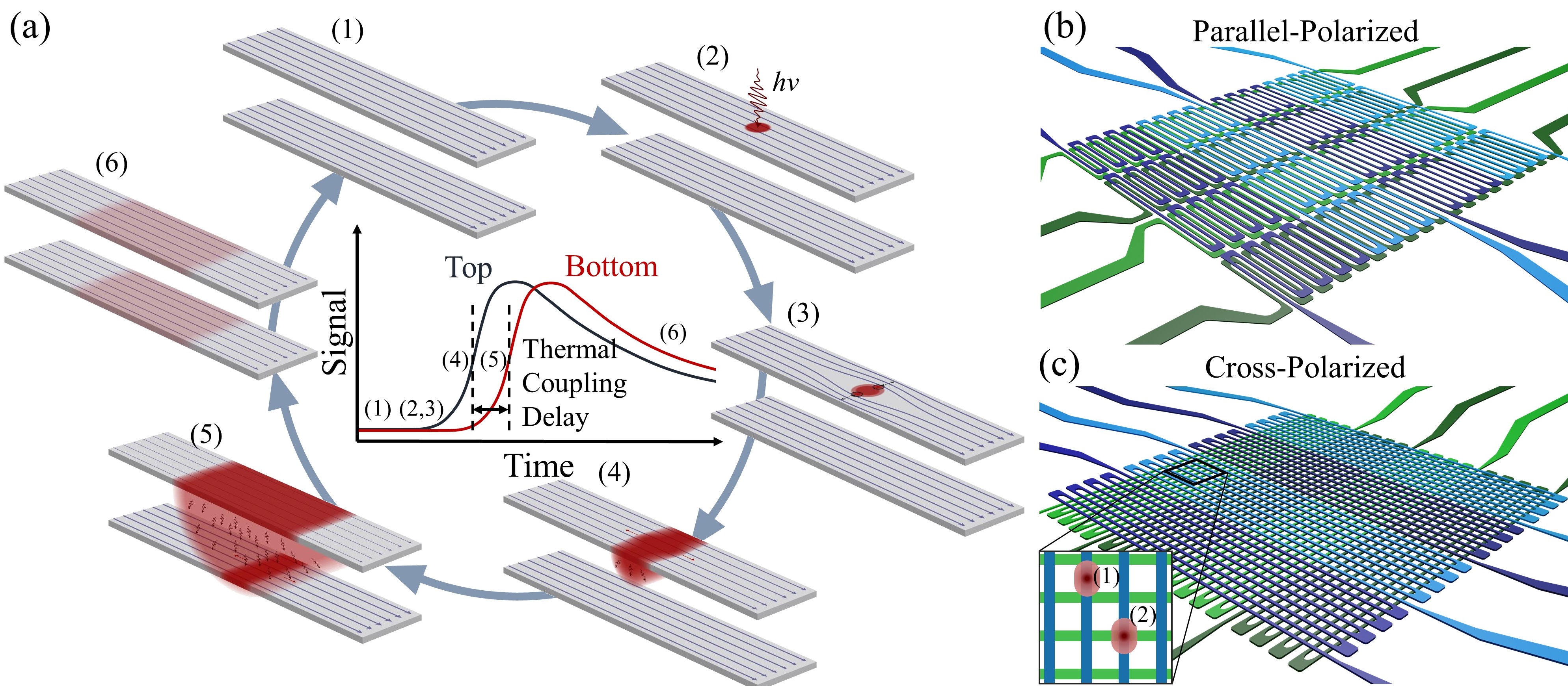
The nanowire orientation can be tailored to suit the needs of a particular application. In the parallel-polarization design shown schematically in Figure 1b, nanowires on both layers are oriented in the same direction and patterned directly above one another. This is ideal for ensuring efficient and fast thermal coupling between the layers, but leads to increased capacitance between pixels which can increase electrical crosstalk. When embedded in a typical optical cavity, the parallel design maintains a strong polarization sensitivity. For applications where this is undesirable, a cross-polarized design can be employed where the nanowires of the two layers are oriented perpendicularly as shown in Figure 1c. This can lead to polarization insensitive optical coupling, and the multilayer design enables broadband absorption with the appropriate optical stack design 26. However, with the cross-polarized design, nanowires are not directly aligned, so the distance heat must travel to trigger the second layer depends on the absorption location. This leads to additional jitter in the thermal coupling time, requiring a larger coincidence window which can impact the MCR (see Supporting Information). Despite this limitation, the overall timing jitter does not suffer in this configuration because the detection jitter is linked only to the first detector to ‘click.’
Two TRC arrays were fabricated; the first uses parallel polarized nanowires as shown schematically in Figure 1b and the second uses perpendicularly polarized nanowires as in Figure 1c. Both devices use wide WSi nanowires on a pitch covering a total active area of by . The full dimensions of the device stack and fabrication details are described in the Supporting Information. All measurements were performed using a temperature-controlled stage of a He-3 sorption fridge. Each of the 8 channels of the arrays was individually biased and measured using a DC coupled cryogenic amplifier chain with an additional room temperature low noise amplifier. Read-out was performed using 8 channels of a 64 channel time-to-digital converter (TDC) with a comparator front end 11, 13. Timetags were saved and analyzed in post-processing, but a real time streaming system could be developed using FPGA based readout.
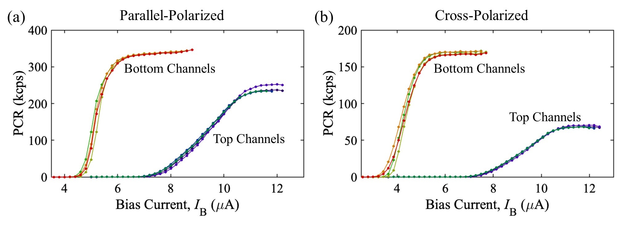
Both styles of device were characterized at a wavelength of in a free-space coupled cryostat. The cryogenic windows of the cryostat include blackbody filters with a total transmission estimated to be greater than 96% at 11. The channels of the bottom layer exhibit a lower switching current than the top layer due to inconsistencies in the fabrication of the two nanowire layers. Despite this, both layers show saturation of internal efficiency for all channels as shown in Figure 2. The number of counts is not distributed evenly between the top and bottom layers due to the properties of the optical cavity, but this distribution is reasonably consistent with rigorous coupled wave analysis (RCWA) modeling of the devices (see Supporting Information).
The TRC concept relies upon efficient thermal coupling between the active layers in order to extract the location where the detection occurred. This requires that every detection on one layer triggers a detection on the other layer. We define the coupling efficiency as the probability that a ‘click’ generated on a channel leads to an unambiguous corresponding ‘click(s)’ on the second layer. An ideal device would only generate a single corresponding detection on the second layer, making the readout as straightforward as possible. If the additional complexity can be handled by the readout processing, triple coincidences (events with detections on three channels within a coincidence window, see Supporting Information) can be tolerated with the understanding that the detection occurred at the region where the pixels meet. This makes the implicit assumption that the probability of two photons being detected at the same time is negligibly small. The coupling probability for the two array designs was characterized using a mode-locked laser for a range of bias currents on both top and bottom layers. For both array types, as the bias currents on both layers approach the switching current, near-unity coupling efficiency is achieved, demonstrating correct operation of the TRC architecture.
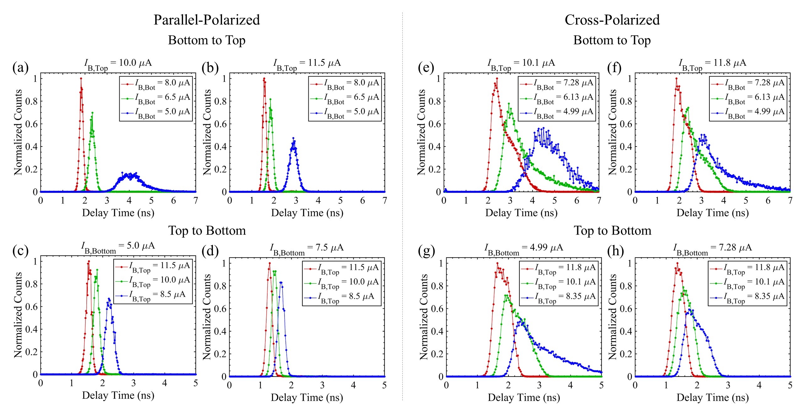
Thermal coupling between layers is not instantaneous. There is a delay on the order of several nanoseconds between associated detection events due to the finite time required for heat to propagate from one nanowire to the second layer. Furthermore, fluctuations in the heat transfer process lead to additional jitter in the detection timing of the second event compared to the first. The coupling delay time is defined as the time difference between the initial detection event and the detection on the second layer. Coupling delay time histograms are shown in Figure 3 for a variety of bias conditions for the two arrays. As can be expected based on the geometry, the parallel-polarized array demonstrates faster coupling and a narrower distribution of coupling times between layers than the cross-polarized device. Differences in the distance heat must propagate to switch the second nanowire layer in the cross-polarized device lead to the appearance of a shoulder and extended long-delay time tail in the coupling behavior. While this effect is diminished at higher bias currents, it is not eliminated completely. Consequently, when compared to the parallel-polarized device, the cross-polarized design requires a wider coincidence window when defining correlated detection events. See the Supporting Information for additional details regarding thermal coupling.
To demonstrate the imaging capability of the TRC devices, we translated a laser spot on the active area of the device using a fast steering mirror. For the cross-polarized device, the spot was directed in a square pattern on the device with varying periods, and the location of the spot was extracted using the centroid of the measured counts. The spot tracking was reliably demonstrated up to limits of the steering mirror speed with period of using frames, with an average of 11.7 photon detections per frame. Figure 4 shows representative sample frames demonstrating this tracking capability, but based on the MCR performance of the device (see Supporting Information), a similar level of tracking accuracy could be achieved at a period with a photon flux increase by a factor 50 with minimal blocking loss.
The TRC architecture is not limited to the WSi material system. For devices which require lower jitter and higher count rates, NbN or NbTiN arrays are possible. The challenge with using these higher materials is ensuring sufficient thermal coupling between the two layers to generate thermally-induced switching. The greater requires that the temperature of the second nanowire layer must be elevated to a higher temperature to switch the device when biased at a given fraction of the nanowire depairing current. While this is not expected to be a problem for the parallel-polarized design, cross-polarized devices may require a high fill factor in order to ensure that there is sufficient overlap between the layers for efficient coupling. A better ability to model heat transfer in thin dielectrics and superconductors is needed to reliably predict the thermal coupling between superconducting nanowire layers in TRC devices.
In conclusion, we have demonstrated a row-column style multiplexing architecture for SNSPD imaging arrays using thermal coupling between two active layers. This new architecture eliminates the current-redistribution and limited fill factor shortcomings of electrically coupled row-column SNSPD arrays. Similar device structures using this platform provide a new means of experimentally probing low temperature heat transfer properties of thin dielectric structures and can be used to produce optimized thermal row-column arrays in the future. The 16-pixel devices characterized in this work are immediately scalable to the kilopixel size for use with existing readout systems and, when integrated with optical cavities, are expected to achieve optical efficiency exceeding 85%. When combined with an additional multiplexing scheme through time domain or standard electrical row-column mechanisms, it will be possible to reach megapixel sized arrays with a manageable number of readout cables. The thermal row-column promises to be a key enabling technology for achieving large area, low intrinsic dark count rate, and high efficiency photon counting imaging systems for low photon flux signals.
1 Associated Content
The Supporting Information includes the fabrication and design details, timing jitter characterization, details of the thermal coupling efficiency, thermal coupling delay times, maximum count rate characterization, and optical efficiency characterization.
2 Acknowledgments
The authors thank V. Verma, A. McCaughan, and S. W. Nam for helpful discussions. This research was performed at the Jet Propulsion Laboratory, California Institute of Technology, under contract with the National Aeronautics and Space Administration. This work was supported by a NASA Space Technology Research Fellowship. Support was provided in part by the DARPA Defense Sciences Office, through the DETECT program.
References
- Gol’tsman et al. 2001 Gol’tsman, G. N.; Okunev, O.; Chulkova, G.; Lipatov, A.; Semenov, A.; Smirnov, K.; Voronov, B.; Dzardanov, A.; Williams, C.; Sobolewski, R. Picosecond superconducting single-photon optical detector. Appl. Phys. Lett. 2001, 79, 705
- Marsili et al. 2013 Marsili, F.; Verma, V. B.; Stern, J. A.; Harrington, S.; Lita, A. E.; Gerrits, T.; Vayshenker, I.; Baek, B.; Shaw, M. D.; Mirin, R. P.; Nam, S. W. Detecting single infrared photons with 93% system efficiency. Nat. Photonics 2013, 7, 210
- Zhang et al. 2017 Zhang, W.; You, L.; Li, H.; Huang, J.; Lv, C.; Zhang, L.; Liu, X.; Wu, J.; Wang, Z.; Xie, X. NbN superconducting nanowire single photon detector with efficiency over 90% at 1550 nm wavelength operational at compact cryocooler temperature. Sci. China Phys. Mech. Astron. 2017, 60, 120314
- Korzh et al. 2018 Korzh, B. A. et al. Demonstrating sub-3 ps temporal resolution in a superconducting nanowire single-photon detector. arXiv 2018, arXiv:1804.06839
- Zadeh et al. 2018 Zadeh, I. E.; Los, J. W. N.; Gourgues, R. B. M.; Bulgarini, G.; Dobrovolskiy, S. M.; Zwiller, V.; Dorenbos, S. N. A single-photon detector with high efficiency and sub-10ps time resolution. arXiv 2018, arXiv:1801.06574
- Caloz et al. 2019 Caloz, M.; Korzh, B.; Ramirez, E.; Schönenberger, C.; Warburton, R. J.; Zbinden, H.; Shaw, M. D.; Bussières, F. Intrinsically-limited timing jitter in molybdenum silicide superconducting nanowire single-photon detectors. J. Appl. Phys. 2019, 126, 164501
- Wollman et al. 2017 Wollman, E. E.; Verma, V. B.; Beyer, A. D.; Briggs, R. M.; Korzh, B. A.; Allmaras, J. P.; Marsili, F.; Lita, A. E.; Mirin, R. P.; Nam, S. W.; Shaw, M. D. UV superconducting nanowire single-photon detectors with high efficiency, low noise, and 4 K operating temperature. Opt. Express 2017, 25, 26792–26801
- Hochberg et al. 2019 Hochberg, Y.; Charaev, I.; Nam, S.-W.; Verma, V.; Colangelo, M.; Berggren, K. K. Detecting Sub-GeV Dark Matter with Superconducting Nanowires. Phys. Rev. Lett. 2019, 123, 151802
- The OST mission concept study team 2018 The OST mission concept study team, The Origins Space Telescope (OST) Mission Concept Study Interim Report. arXiv 2018, arXiv:1809.09702
- McCarthy et al. 2013 McCarthy, A.; Krichel, N. J.; Gemmell, N. R.; Ren, X.; Tanner, M. G.; Dorenbos, S. N.; Zwiller, V.; Hadfield, R. H.; Buller, G. S. Kilometer-range, high resolution depth imaging via 1560 nm wavelength single-photon detection. Opt. Express 2013, 21, 8904–8915
- Shaw et al. 2017 Shaw, M. D.; Marsili, F.; Beyer, A. D.; Briggs, R. M.; Allmaras, J. P.; Farr, W. H. Superconducting nanowire single photon detectors for deep space optical communication (Conference Presentation). Proc. SPIE 2017, 100960J
- Allman et al. 2015 Allman, M. S.; Verma, V. B.; Stevens, M.; Gerrits, T.; Horansky, R. D.; Lita, A. E.; Marsili, F.; Beyer, A.; Shaw, M. D.; Kumor, D.; Mirin, R.; Nam, S. W. A near-infrared 64-pixel superconducting nanowire single photon detector array with integrated multiplexed readout. Appl. Phys. Lett. 2015, 106, 192601
- Wollman et al. 2019 Wollman, E. E.; Verma, V. B.; Lita, A. E.; Farr, W. H.; Shaw, M. D.; Mirin, R. P.; Woo Nam, S. Kilopixel array of superconducting nanowire single-photon detectors. Opt. Express 2019, 27, 35279
- Miyajima et al. 2019 Miyajima, S.; Yabuno, M.; Miki, S.; Terai, H. Single-Flux-Quantum Based Event-Driven Encoder for Large-Pixel Superconducting Nanowire Single-Photon Detector Array. IEEE Trans. Appl. Supercond. 2019, 29, 1–4
- Miyajima et al. 2018 Miyajima, S.; Yabuno, M.; Miki, S.; Yamashita, T.; Terai, H. High-time-resolved 64-channel single-flux quantum-based address encoder integrated with a multi-pixel superconducting nanowire single-photon detector. Opt. Express 2018, 26, 29045–29054
- Zhao et al. 2017 Zhao, Q.-Y.; Zhu, D.; Calandri, N.; Dane, A. E.; McCaughan, A. N.; Bellei, F.; Wang, H.-Z.; Santavicca, D. F.; Berggren, K. K. Single-photon imager based on a superconducting nanowire delay line. Nat. Photonics 2017, 11, 247
- Zhu et al. 2018 Zhu, D.; Zhao, Q.-Y.; Choi, H.; Lu, T.-J.; Dane, A. E.; Englund, D.; Berggren, K. K. A scalable multi-photon coincidence detector based on superconducting nanowires. Nat. Nanotechnol. 2018, 13, 596–601
- Zhu et al. 2019 Zhu, D.; Colangelo, M.; Korzh, B. A.; Zhao, Q.-Y.; Frasca, S.; Dane, A. E.; Velasco, A. E.; Beyer, A. D.; Allmaras, J. P.; Ramirez, E.; Strickland, W. J.; Santavicca, D. F.; Shaw, M. D.; Berggren, K. K. Superconducting nanowire single-photon detector with integrated impedance-matching taper. Appl. Phys. Lett. 2019, 114, 042601
- Van Rantwijk et al. 2016 Van Rantwijk, J.; Grim, M.; van Loon, D.; Yates, S.; Baryshev, A.; Baselmans, J. Multiplexed Readout for 1000-Pixel Arrays of Microwave Kinetic Inductance Detectors. IEEE Trans. Microwave Theory Techn. 2016, 64, 1876–1883
- Meeker et al. 2018 Meeker, S. R. et al. DARKNESS: A Microwave Kinetic Inductance Detector Integral Field Spectrograph for High-contrast Astronomy. PASP 2018, 130, 065001
- Szypryt et al. 2017 Szypryt, P.; Meeker, S. R.; Coiffard, G.; Fruitwala, N.; Bumble, B.; Ulbricht, G.; Walter, A. B.; Daal, M.; Bockstiegel, C.; Collura, G.; Zobrist, N.; Lipartito, I.; Mazin, B. A. Large-format platinum silicide microwave kinetic inductance detectors for optical to near-IR astronomy. Opt. Express 2017, 25, 25894–25909
- Sinclair et al. 2019 Sinclair, A. K.; Schroeder, E.; Zhu, D.; Colangelo, M.; Glasby, J.; Mauskopf, P. D.; Mani, H.; Berggren, K. K. Demonstration of microwave multiplexed readout of DC biased superconducting nanowire detectors. IEEE Trans. Appl. Supercond. 2019, 29, 1–4
- Doerner et al. 2017 Doerner, S.; Kuzmin, A.; Wuensch, S.; Charaev, I.; Boes, F.; Zwick, T.; Siegel, M. Frequency-multiplexed bias and readout of a 16-pixel superconducting nanowire single-photon detector array. Appl. Phys. Lett. 2017, 111, 032603
- Kerman et al. 2009 Kerman, A. J.; Yang, J. K. W.; Molnar, R. J.; Dauler, E. A.; Berggren, K. K. Electrothermal feedback in superconducting nanowire single-photon detectors. Phys. Rev. B 2009, 79, 100509
- Verma et al. 2016 Verma, V. B.; Lita, A. E.; Stevens, M. J.; Mirin, R. P.; Nam, S. W. Athermal avalanche in bilayer superconducting nanowire single-photon detectors. Appl. Phys. Lett. 2016, 108, 131108
- Verma et al. 2012 Verma, V. B.; Marsili, F.; Harrington, S.; Lita, A. E.; Mirin, R. P.; Nam, S. W. A three-dimensional, polarization-insensitive superconducting nanowire avalanche photodetector. Appl. Phys. Lett. 2012, 101, 251114