Binding and Electronic Level Alignment of -Conjugated Systems on Metals
Abstract
We review the binding and energy level alignment of -conjugated systems on metals, a field which during the last two decades has seen tremendous progress both in terms of experimental characterization as well as in the depth of theoretical understanding. Precise measurements of vertical adsorption distances and the electronic structure together with ab-initio calculations have shown that most of the molecular systems have to be considered as intermediate cases between weak physisorption and strong chemisorption. In this regime, the subtle interplay of different effects such as covalent bonding, charge transfer, electrostatic and van der Waals interactions yields a complex situation with different adsorption mechanisms. In order to establish a better understanding of the binding and the electronic level alignment of -conjugated molecules on metals, we provide an up-to-date overview of the literature, explain the fundamental concepts as well as the experimental techniques and discuss typical case studies. Thereby, we relate the geometric with the electronic structure in a consistent picture and cover the entire range from weak to strong coupling.
I Introduction
The interface between -conjugated organic semiconductor molecules and metals is at the heart of a number of important scientific questions, both from a fundamental as well as from an applied perspective. It is a key issue for the different energy-level alignment (ELA) schemes as well as for charge carrier injection/extraction efficiencies and related issues in organic (opto)electronics devices Ishii_1999_AdvMater; Kahn_2003_JPolymSciBPolymPhys; Koch_2008_JPhysCondensMatter; Widdascheck_2019_AdvFunctMater; Fahlman_2019_NatRevMater. At the same time, already the question of the interaction and binding is non-trivial, in particular, for systems which are between the limiting cases of (clearly weak) physisorption and (clearly strong) chemisorption. Importantly, there is a subtle interplay between geometric and electronic structure, with a frequently substantial (but not necessarily dominating) contribution of dispersion interactions, which makes predictions of the metal-organic interface rather challenging, if only “simple rules” are employed. Rather advanced theoretical methods, developed in the last decade, have enabled substantial progress Tkatchenko_2010_MRSBulletin; Berland_2015_RepProgPhys; Liu_2015_PhysRevLett; Maurer_2016_ProgSurfSci; Hermann_2017_ChemRev; Liu_2017_JChemPhys. In parallel with that, a satisfactory understanding of these systems requires the experimental determination of both the exact adsorption (i.e., binding) geometry as well as the resulting electronic structure including possible charge transfer, interface dipoles, and shifts of the electronic levels. Fortunately, the last years have also seen tremendous progress in experimental results, so that we are now looking at a reasonably large and representative set of experimental data on a number of systems, which allow a more comprehensive discussion. This is the main goal of the present review.
We shall first emphasize the importance of the structural properties. In line with the motivation above, it has become clear that the precise knowledge of the molecular arrangement on the surface is necessary to assess and interpret the electronic properties and eventually the ELA. The nature of the interaction of (aromatic) -systems with metals is less obvious than, say, CO on Ni(111) or other chemisorbing systems Norsko_1990_RepProgPhys, which can be safely assumed to exhibit a well-established chemical bond on the one hand, and, say, noble gases, which are obviously physisorption, i.e. dispersion-interaction dominated on the other hand Diehl_2004_JPhysCondensMatter. The interaction and interface for the intermediate case has been subject to intense research with two largely complementary approaches:
-
I.
Experimental high-precision determination of adsorption distances, mostly using the X-ray standing wave (XSW) technique. Remarkably, while XSW had been developed in the 1960s for the localization of interstitial dopants in the bulk Zegenhagen_1993_SurfSciRep and thereafter used also for simple adsorbates on surfaces Cowan_1980_PhysRevLett; Bedzyk_1985_PhysRevB, the first investigations of larger aromatic compounds were published only in 2005 Gerlach_2005_PhysRevB; Hauschild_2005_PhysRevLett. Since then, numerous studies using the XSW technique have revealed that -conjugated molecules on metals show a surprisingly rich phenomenology, e.g., with significant distortions of the molecules on noble metal surfaces. Of course, also other techniques such as photoelectron diffraction (PhD) Hofmann_1994_SurfSci, rod-scans in X-ray diffraction Krause_2003_JChemPhys or LEED I-V Stellwag_1995_SurfSci; Zheleva_2012_JPhysChemC; Sirtl_2013_PhysChemChemPhys, which are used for structural investigations on surfaces, have their merits but do not exhibit the same precision and/or element specificity as the XSW technique.
-
II.
Quantum theoretical calculations that managed to include long-range dispersion forces in density functional theory (DFT) codes Grimme_2006_JComputChem; Rydberg_2003_PhysRevLett; Dion_2004_PhysRevLett; Tkatchenko_2009_PhysRevLett; Berland_2019_PhysRevB, which became more popular than previous attempts involving, e.g., Hartree-Fock self-consistent field wave functions Bagus_2002_PhysRevLett or Møller-Plesset perturbation theory (MP2) Abbasi_2009_JPhysChemC. Different schemes going beyond standard DFT were developed to tackle the fundamental problem, how to treat exchange-correlation effects. While those approximations with dispersion corrections involve increased computational costs, they have become more and more accurate for calculating the adsorption geometry of organic molecules on metals. In this context, the reader seeking more information is referred to reviews of vdW-corrected DFT Klimevs_2012_JChemPhys; Berland_2015_RepProgPhys; Hermann_2017_ChemRev and to Ref. Maurer_2016_ProgSurfSci for its application in the context of metal-organic interfaces.
Regarding the electronic properties of such systems, it has already been recognized in the 1970s that the electronic structure of molecular solids is considerably different to that in the gas phase Seki_1974_BullChemSocJpn; Salaneck_1978_PhysRevLett. However, it took twenty more years until “energy-level alignment” and “interface dipoles” for -systems at interfaces came into the focus of research Ohno_1991_PhysRevB; Narioka_1995_ApplPhysLett; Lee_1998_ApplPhysLett and the seminal review by Ishii et al. has been published Ishii_1999_AdvMater. In the last decade a systematic understanding and phenomenology has been established Kahn_2003_JPolymSciBPolymPhys; Koch_2007_ChemPhysChem; Braun_2009_AdvMater; Hwang_2009_MaterSciEngR; Greiner_2012_NatMater; Opitz_2017_JPhysCondensMatter; Cinchetti_2017_NatMater; Akaike_2018_JpnJApplPhys Zojer_2019_AdvMaterInterfaces. In particular, ELA is now relatively well studied for multilayers on inert substrates, i.e., if substrate-adsorbate interactions can be neglected Ley_2013_AdvFunctMater; Oehzelt_2014_NatCommun; Yang_2017_JPhysDApplPhys. However, this is frequently not the case on metal substrates, and it is clear that the complete binding scenario including possible distortions of the adsorbate is required for a thorough understanding of ELA Koch_2008_JPhysCondensMatter; Monti_2012_JPhysChemLett; Klappenberger_2014_ProgSurfSci; Goiri_2016_AdvMater; Otero_2017_SurfSciRep.
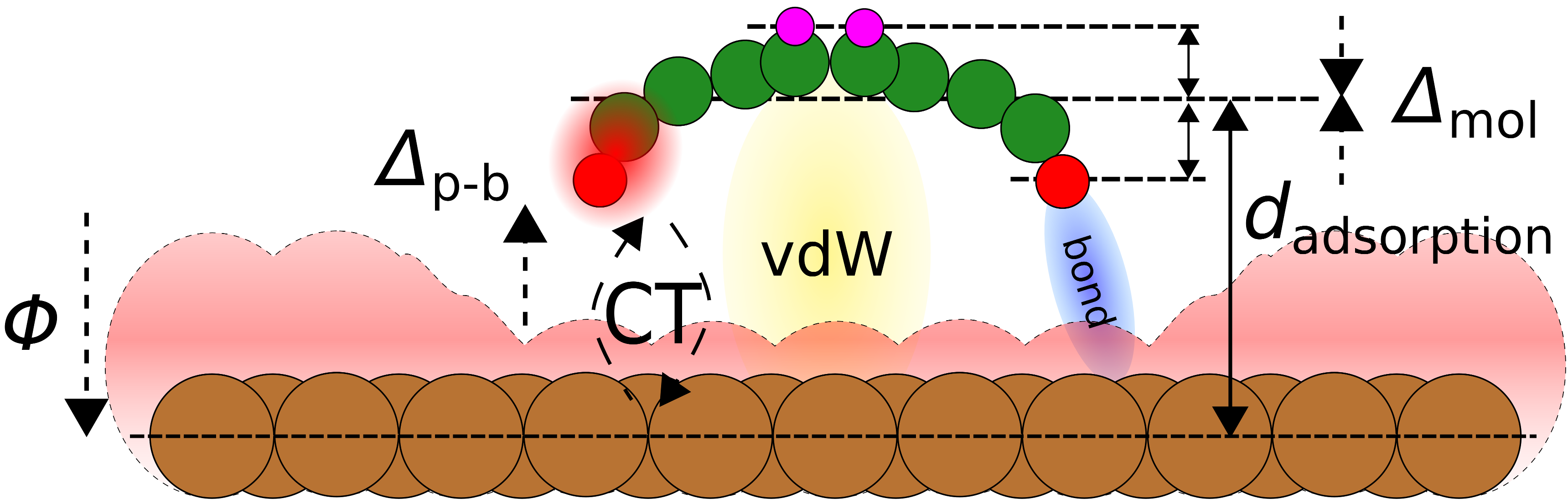
As mentioned above, it is by now accepted that ELA at organic-metal interfaces is of utmost importance for the performance of organic (opto)electronic devices Fung_2016_AdvMater; Lussem_2016_ChemRev; Nakano_2017_AdvMater; Opitz_2017_JPhysCondensMatter; Akaike_2018_JpnJApplPhys; Bao_2019_AdvMaterInterfaces; Rockson_2019_ACSApplMaterInterfaces; Gurney_2019_RepProgPhys. Moreover, energy-levels and thus charge injection barriers can be tuned by engineering the substrate work function Koch_2005_PhysRevLett; Li_2009_ChemMater; Zhou_2012_Science; Vilan_2017_ChemRev; Widdascheck_2019_AdvFunctMater. This can be done by pre-covering a metal electrode with a monolayer of an electron acceptor (donor) for increasing (decreasing) the effective substrate work function and thus lowering the hole (electron) injection barrier into subsequently deposited organic layers Koch_2005_PhysRevLett; Broker_2008_ApplPhysLett; Rana_2012_PhysStatSolA; Gao_2013_ApplPhysLett; Timpel_2018_AdvFunctMat. The contact formation at such strongly coupled interfaces goes usually along with a complex electronic scenario involving donation and back-donation of charges (see Figure 1) Romaner_2007_PhysRevLett; Tseng_2010_NatChem; Vitali_2010_NatMater; Haming_2012_PhysRevB; Hofmann_2013_NewJPhys; Stadtmuller_2014_NatComms; Zamborlini_2017_NatCommun; Chen_2019_JPhysCondensMatter. Furthermore, the adsorption distances including a possible intramolecular distortion impacting the molecular dipole are essential. This is why in-depth discussion of the electronic structure usually requires a precise determination of the geometric structure (Figure 1), and why XSW results have a key role in this context. Several original research articles (e.g. Refs. Romaner_2007_PhysRevLett; Koch_2008_JAmChemSoc; Duhm_2008_OrgElec; Stadler_2009_NaturePhysics; Kroger_2010_NewJPhys; Heimel_2013_NatureChem; Stadtmuller_2014_NatComms; Baby_2017_ACSNano; Franco-Canellas_2017_PhysRevMaterials; Klein_2019_JPhysChemC; Chen_2019_JPhysCondensMatter) and, more recently, some review articles and book contributions (Refs. Gerlach_2013_book; Stadtmuller_2015_JElectronSpectroscRelatPhenom; Duhm_2015_chapter; Willenbockel_2014_PhysChemChemPhys; Maurer_2016_ProgSurfSci; Otero_2017_SurfSciRep; Kera_2018_JPhysSocJpn) have demonstrated that correlating electronic structure and vertical adsorption heights gives new insights.
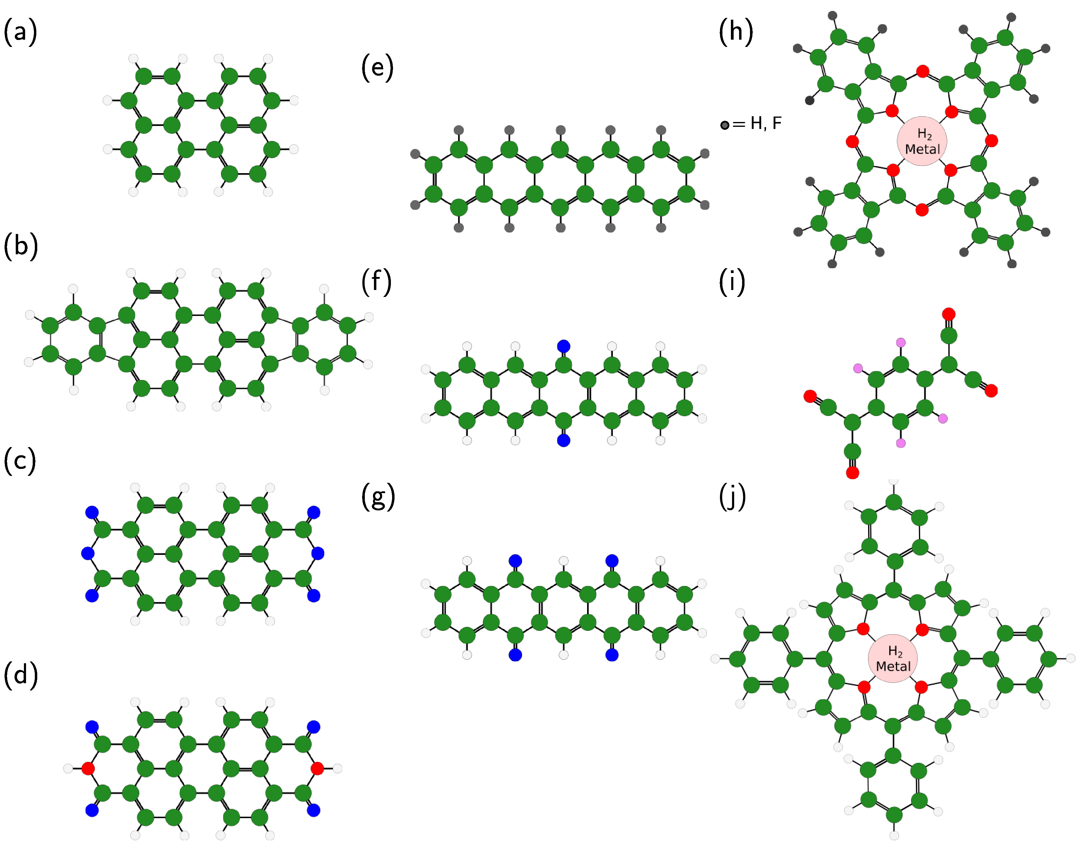
This review is organized as follows: Initially, we explain the basic concepts of organic-metal contact formation (Sec. II), followed by some experimental considerations related to XSW, photoelectron spectroscopy and complementary techniques (Sec. III). After providing a comprehensive list of XSW data obtained for conjugated organic molecules (COMs, representative chemical structures are shown in Figure 2) on metals, which may serve as reference and general overview, we discuss several typical adsorbate systems (Sec. LABEL:sec:case_studies). In each case, we explore the geometric and electronic structure of these systems as well as how these properties are related for different adsorption scenarios. Finally, we shall summarize the important findings (Sec. LABEL:sec:summary).
II General considerations and fundamentals
First, we shall introduce the basic quantities, concepts and phenomena that describe and govern the metal-organic interface, in particular with respect to the different effects influencing the ELA in the monolayer regime.
II.1 Interface energetics
The most relevant energy-levels at an organic-metal interface in the limiting case of physisorption are shown in Figure 3. A metal has electrons occupying energy-levels up to the Fermi level . The energy to bring them to the vacuum level (VL) corresponds to the metal work function . In the COM the most important energy-levels are those of the highest occupied molecular orbital (HOMO) and the lowest unoccupied molecular orbital (LUMO), which are also referred to as the frontier molecular orbitals. The energy difference between the HOMO and the LUMO defines the transport gap . Because typical exciton binding energies of COM thin films are in the range of several hundred meV Friend_2012_FaradayDiscuss; Forrest_2015_PhilTansRSocA; Djurovich_2009_OrgElec, i.e. much higher than for most inorganic semiconductors, the optical gap is considerably smaller than Gao_2001_ApplPhysLett; Zahn_2007_ChemRev; Bredas_2014_MaterHoriz, with the latter being the relevant parameter for ELA and the charge-transport characteristics of the thin film. We note that the ionization energy (IE), which is defined as the energy necessary to move an electron from the HOMO to the vacuum, and the electron affinity (EA), which is the energy necessary to bring an electron from the vacuum to the LUMO, cannot be considered as materials parameters: The collective impact of intramolecular dipole moments, which depend on the molecular orientation within the thin film, influences the IE as well as the EA Han_2013_ApplPhysLett; Heimel_2011_ChemMater; Duhm_2008_NatMater; DAvino_2016_JPhysCondensMatter. Therefore, one has to determine these values for each specific thin film structure.
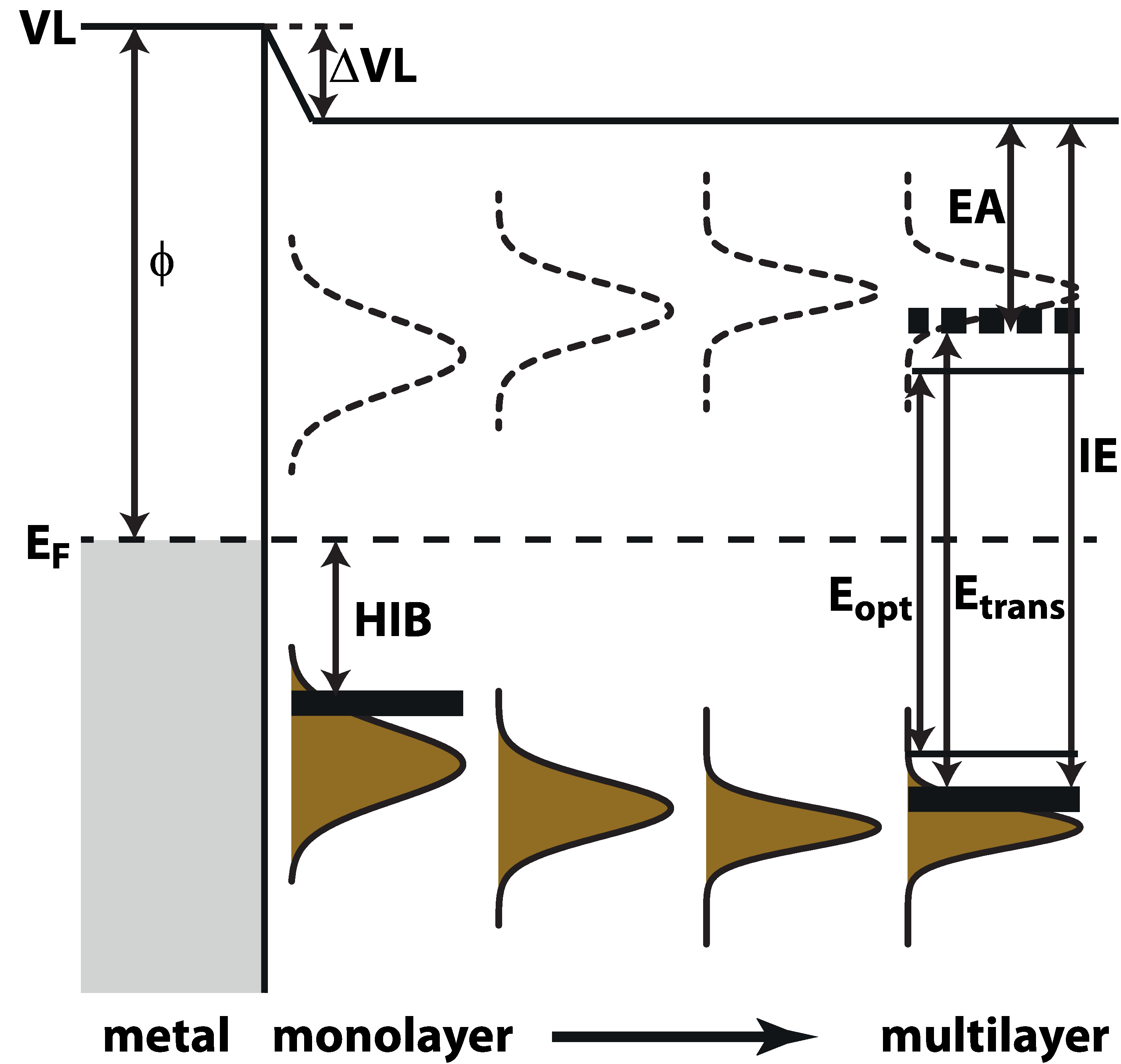
For the IE and EA often the onsets of experimentally determined HOMO and LUMO levels are used Kahn_2003_JPolymSciBPolymPhys; Zahn_2006_ChemPhys, (cf. Figure 3) because the onsets govern the transport properties Horowitz_2015_JApplPhys. However, the onset of a peak measured by (inverse) photoemission depends, naturally, on the experimental resolution. Furthermore, the signal-to-noise-ratio can also play a significant role for the onset, especially if the peak shape is not simply Gaussian and/or gap states are involved Zu2019JPhysChemLett; Yang_2017_JPhysDApplPhys. Whether the use of onsets or peak maxima is more beneficial depends on the specific adsorbate/substrate system and the scientific question. Unfortunately, no general convention has been established yet and, consequently, great care has to be taken when comparing values from different publications or when comparing experiment and theory.
For COM thin films polarization leads to a rearrangement of energy-levels in the solid state compared to the gas phase Hill_2000_ChemPhysLett; Schwoerer_2007_book; DAvino_2016_JPhysCondensMatter; Liu_2017_JChemPhys; Li_2018_PhysRevB. The polarizability of metals is, in general, much higher than that of organic thin films. The image-charge effect (often called screening) leads thus to a further narrowing of the transport gap in monolayers on a metal substrate compared to multilayers Hill_2000_JApplPhys; Koch_2007_ChemPhysChem as shown in Figure 3. Moreover, even for physisorption the vicinity of a metal leads to broadening of the energy-levels through electronic, quantum-mechanical interaction of the localized molecular states with the continuum of metal states Anderson_1961_PhysRev; Heimel_2016_chapter; Willenbockel_2014_PhysChemChemPhys.
Upon contact formation of a COM and a metal, vacuum level alignment is rather the exception than the rule Li_2017_AdvMater; Koch_2008_JPhysCondensMatter; Kahn_2003_JPolymSciBPolymPhys; Braun_2009_AdvMater; Ishii_1999_AdvMater; Egger_2015_NanoLett; Akaike_2018_JpnJApplPhys. There are various reasons for vacuum level shifts VL upon contact formation, which are not restricted to metal substrates, but may also take place when the molecules are adsorbed on inorganic semiconductors and insulators Greiner_2012_NatMater; Hewlett_2016_AdvMater; Fu_2018_ACSApplMaterInterfaces; Erker_2019_JPhysChemLett; Futscher_2019_JPhysCondensMatter. The magnitude of interface dipoles is often related to vertical adsorption distances and the most relevant possible contributions as they are illustrated in Figure 4 are:
-
I.
Push-back effect caused by the Pauli repulsion between the electrons of the adsorbate and the metal
-
II.
Charge transfer between adsorbate and substrate
-
III.
Chemical bond formation between adsorbate and substrate
-
IV.
Molecular dipole moment , which can be intrinsic (polar COMs) or due to adsorption induced distortions
For the physisorbed system shown in Figure 3 only the push-back effect is considered. For systems with stronger interactions the impact of the interfacial coupling on VL has to be taken into account. In general, whether an adsorbate is physisorbed or chemisorbed on a substrate is clearly defined by adsorption energies Atkins_2006_book and can be accessed theoretically Liu_2013_NatCommun; Jakobs_2015_NanoLett; Maurer_2016_ProgSurfSci; Hollerer_2017_ACSNano; Sarkar_2018_ChemMater; Yang_2018_ACSApplMaterInterfaces. However, the adsorption type is not directly accessible by standard experimental techniques. To overcome this issue we use a simple definition based on peak shifts between mono- and multilayer in photoemission data Wang_2018_JPhysChemC: For rigid shifts of valence electron features (typically the HOMO-derived peak) and core-levels we assume physisorption and chemisorption in all other cases. Within this definition it becomes apparent that the pentacene oxo-derivative P2O is physisorbed on Ag(111) and P4O is chemisorbed on the same substrate. Thus, we use schematic energy-level diagrams based on photoemission data Heimel_2013_NatureChem; Wang_2018_JPhysChemC of P2O and P4O on Ag(111) (Figure 5) to illustrate the impact of organic-metal coupling strength on interface dipoles and ELA.
The push-back effect, which leads to , is related to the electron density spilling out into vacuum at clean metal surfaces Wandelt_1997_ApplSurfSci; Smoluchowski_1941_PhysRev; Witte_2005_ApplPhysLett. Push-back takes place at virtually all organic-metal interfaces as the surface dipole part of the metal work function will be decreased by the mere presence of the molecular monolayer Bagus_2002_PhysRevLett; DeRenzi_2005_PhysRevLett; Koch_2007_ChemPhysChem. There is a clear correlation between and adsorption distances Rusu_2010_PhysRevB; Egger_2015_NanoLett; Toyoda_2010_JChemPhys; Ferri_2017_PhysRevMaterials. For physisorbed systems the push-back effect is often the main contribution to VL and can be held responsible for most of the 0.60 eV shift at the P2O/Ag(111) interface.
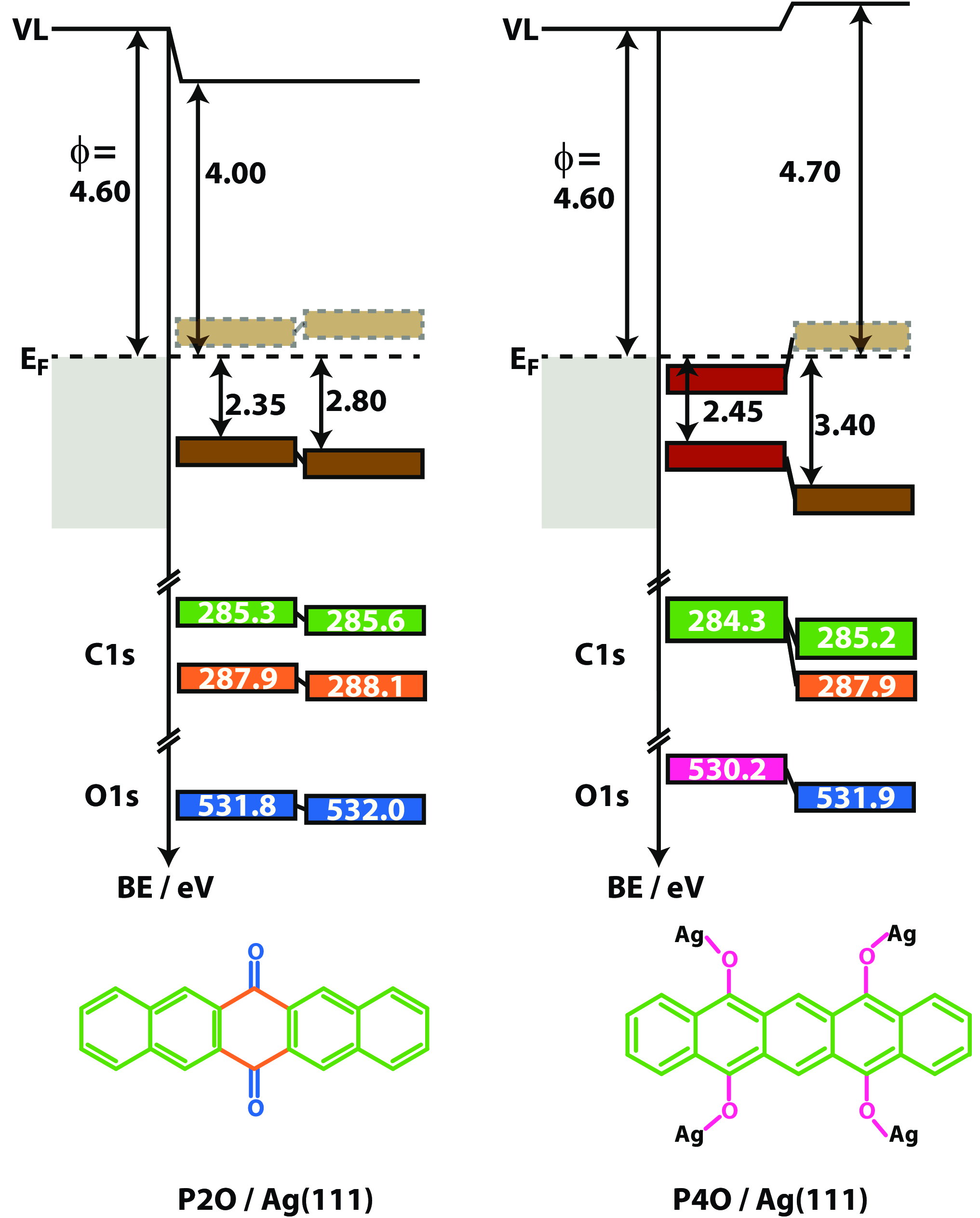
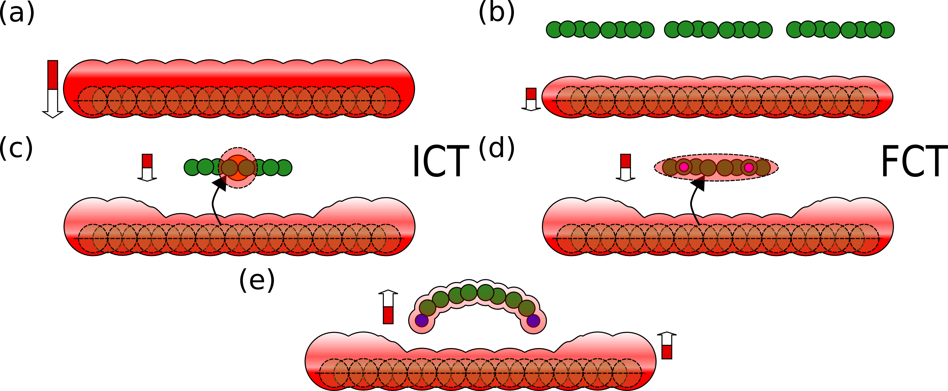
For the discussion of interfacial charge transfer it is helpful to distinguish between integer and fractional charge transfer (Figure 4c and d) Winkler_2015_MaterHoriz; Hollerer_2017_ACSNano; Hofmann_2015_ACSNano. While the latter is usually related to chemical bond formation, the former can also occur for weakly interacting systems and is then a result of Fermi level pinning Braun_2009_AdvMater; Khoshkhoo_2017_OrgElec. This happens for high (or low) substrate work functions for which a vacuum level controlled ELA would lead to a situation with the HOMO (LUMO) being above (below) the Fermi level. In such cases thermodynamic equilibrium is maintained by an interfacial charge transfer. Thus, notably, also in the absence of any specific interfacial interaction charge transfer across an organic-inorganic interface can take place. Interestingly, the HOMO- (LUMO-) levels are typically pinned several hundred meV below (above) Braun_2009_AdvMater; Ley_2013_AdvFunctMater; Oehzelt_2014_NatCommun; Yang_2017_OrgElec; Horowitz_2015_JApplPhys; Fukagawa_2007_AdvMater. This is due to a certain degree of disorder in molecular thin films leading to a broadening of HOMO and LUMO density-of-states (DOS) Oehzelt_2014_NatCommun; Yang_2017_JPhysDApplPhys. The relationship between DOS shape and ELA has been addressed in several publications Zuo_2016_PhysRevB; Horowitz_2015_JApplPhys; Kalb_2010_PhysRevB; Oehzelt_2014_NatCommun; Yang_2017_JPhysDApplPhys and is beyond the scope of this review. Likewise, for ELA at organic-organic interfaces, the reader is referred to Refs. Tang_2007_JApplPhys; Braun_2009_AdvMater; Poelking_2014_NatMater; Chen_2011_AdvFunctMater; Opitz_2017_JPhysCondensMatter; Li_2017_AdvMater; Oehzelt_2015_SciAdv.
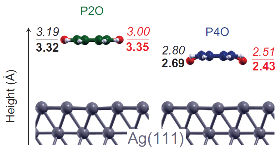
The above mentioned screening effect leads to rigid energy-level shifts (typically several hundred meV) of valence and core-levels to higher binding energies between monolayer and multilayer coverage of organic thin films Hill_2000_JApplPhys; Koch_2007_ChemPhysChem. This is the case for physisorbed P2O on Ag(111) (Figure 5). For chemisorbed systems, the expected shifts due to screening can be overcompensated by the strong chemical coupling at the organic-metal interface. This becomes apparent for P4O on Ag(111); in this particular case, chemisorption goes along with a filling of the former LUMO. The charge transfer counteracts the VL decrease by push back leading to a constant VL upon contact formation. The apparent vacuum level alignment is, however, most likely coincidental. For related systems also a pronounced increase in the effective metal work function has been observed Duhm_2006_JPhysChemB; Kawabe_2008_OrgElec; Koch_2005_PhysRevLett. Such systems will be discussed in more detail in Sec. LABEL:sec:CTC. The relatively strong chemisorption of P4O on Ag(111) leads to a rehybridization of the molecules in the monolayer (a possible resonance structure is shown in the bottom of Figure 5). This is in line with the experimentally determined vertical adsorption distances (Figure 6), which show a pronounced distortion of P4O upon adsorption on Ag(111) Heimel_2013_NatureChem.
Overall, the PxO/Ag(111) systems (Figure 5) demonstrate some potential pitfalls in interpreting energy-level diagrams: For P2O/Ag(111) an apparent interface dipole mimics strong interaction, whereas the charge transfer at the P4O/Ag(111) interface leads to apparent vacuum level alignment. Thus, additional information is necessary to fully understand and describe organic-metal interface energetics. In particular, a precise knowledge of the vertical adsorption distance is necessary for a proper description of the adsorption behavior.
II.2 Role of the substrate
As discussed above, one can distinguish two limiting cases within the domain of metal-organic interactions, namely, physisorption and chemisorption. The adsorption distances are therefore expected to range between the sum of the van der Waals radii for pure physisorptive bonding and the sum of the covalent radii for pure chemisorptive bonding. The corresponding values for carbon atoms interacting with the three noble metals are given in Tab. 1. Obviously, the differences between van der Waals and covalent bonding for a given substrate material (being Å) are much larger than the differences related to the choice of the substrate, i.e. Cu, Ag or Au. XSW experiments, however, consistently show that typical adsorption distances on these substrates are not similar and that the different reactivity of those materials is a key factor. For that purpose, the electronic properties of the substrates have to be discussed in some detail Brivio_1999_RevModPhys.
| (Å) | (Å) | (Å) | (keV) | (eV) | (111) surface | ||
|---|---|---|---|---|---|---|---|
| Cu | 29 | 3.17 | 2.08 | 2.086 | 2.972 | 4.9 | small relaxation Lindgren_1984_PhysRevB |
| Ag | 47 | 3.49 | 2.21 | 2.357 | 2.630 | 4.6 | small relaxation Statiris_1994_PhysRevLett |
| Au | 79 | 3.43 | 2.12 | 2.353 | 2.634 | 5.3 | herringbone reconstruction Takeuchi_1991_PhysRevB; Sandy_1991_PhysRevB |
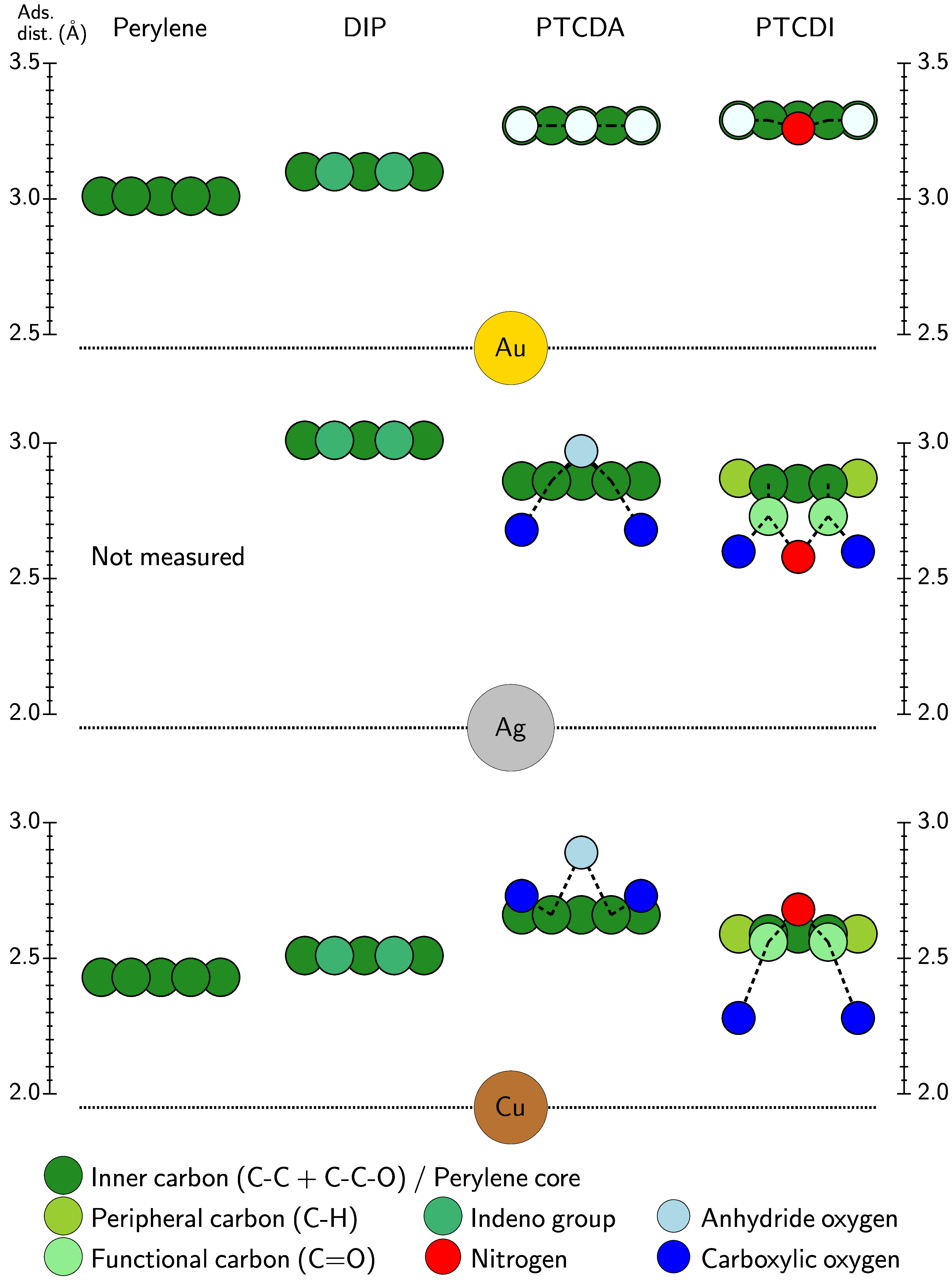
In metals, narrow - and broad -bands form the valence-band states, where the latter are more likely to interact with a given adsorbate. At a certain distance, the molecular orbitals will start to overlap with those of the surface atoms. Initially, the adsorbate orbitals will broaden and shift in energy (see Figure 3) as a consequence of the interactions with the rather delocalized -electrons and only if the -orbitals are involved will the adsorbate levels split into bonding and antibonding states, generally one being below and the other above the metal band. In this context, one can relate the interaction strength and the degree of chemisorption to the different orbitals involved. For instance, the term weak chemisorption is used for the case where only -orbitals are involved. When -orbitals are also at play, the filling of the bonding and antibonding states influences the interaction strength as well. Thus, a strong bond is associated to the filling of only bonding states. Conversely, the partial or total filling of antibonding states induces a repulsive interaction that counteracts the attractive forces exerted by the -electrons. The degree of filling is related to the relative position of the -states with respect to the Fermi level. Also, the broadening of these states is responsible for the degree of repulsion with the adsorbate states. Indeed, a broader state increases the overlap with the adsorbate orbitals and subsequently the cost of orthogonalizing the wave functions to avoid Pauli repulsion. In light of this, moving from left to right in the periodic table, i.e. from transition to coinage metals, the outmost -states shift down in energy away from the Fermi level Hammer_1995_Nature, thus explaining the decreasing reactivity within this series. The broadening of the band, on the other hand, increases when moving down the column or from right to left in the periodic table, which explains why Cu is said to be more reactive than Au. This trend is also reflected in the averaged vertical adsorption distances of the carbon atoms in the molecular backbone of adsorbates on such surfaces. Figure 7 shows that decreases for each perylene derivative on the (111)-surfaces of noble metals in the order Au–Ag–Cu. This finding can be considered as a qualitative trend for most COMs on these surfaces, but precise quantitative predictions can only be done if the nature of the adsorbate is taken into account.
For the interaction with a given adsorbate, not only the chemical composition of the bulk crystal is important, but also its surface structure and termination. Both the transfer of charge across the interface and the formation of bonds often need some energy barriers to be overcome. For all metal substrates the work function decreases with increasing “openness” of the surface being considered. Thus, closed-packed surface structures, i.e. fcc(111), bcc(110), and hcp(001), show the highest and the lowest reactivity. Likewise, defects, step edges and kinks act as interaction centers for adsorbates, which in some cases migrate across the flat terraces until they find a suitable location. In all these cases, the electronic and/or chemical interaction, with the extreme case of adsorbate dissociation, is favored by the lower energy barriers caused by elements that disrupt the surface potential landscape due to dangling bonds or excess/defect of charges, which may be recovered by the interaction with the adsorbate.
Of particular importance for CT effects is the presence of surface states, which form as a consequence of the reduced coordination of the topmost atoms compared to those in the bulk Shockley_1939_PhysRev; Reinert_2001_PhysRevB. Due to the termination of the crystal and the change of the electronic band structure new states confined to a region very close to the surface may exist. While these states appear even on perfect surfaces, the presence of defects, impurities or even adsorbates may create new interface states localized around them. Similar to the doping in semiconductors, surface/interface states may act as a center for charge exchange or reaction when a certain adsorbate is present.
In the context of this review, a large fraction of the studies in the literature have focused on the (111)-surfaces of Au, Ag and Cu. These are relatively inert and less prone to reacting with aromatic adsorbates. Also, for the noble metals they are the ones with the lowest energy, meaning that they are preferred in evaporation processes, giving them a slightly higher practical relevance than, e.g., (110) and (100). Recently, also other orientations of the noble metals Mercurio_2013_PhysRevB; Weiss_2017_PhysRevB; Felter_2019_Nanoscale, alloys Bauer_2016_PhysRevB; Stadtmueller_2019_JPhysCondensMatter as well as ZnO Hewlett_2016_AdvMater; Erker_2019_JPhysChemLett; Niederhausen_2020_PhysRevMaterials have been investigated, see the list in Sec. LABEL:sec:case_studies. For more details on the substrate surface without adsorbates, we refer to Ref. Woodruff_2010_JPhysCondensMatter
II.3 Role of the molecule
The description of organic molecules is largely based on the concept of localized bonds Bader_1991_ChemRev. On metal surfaces, however, this approach might be questioned and is scrutinized, e.g., by specific chemical modifications of the -conjugated systems being investigated. It is well known and understood how functional groups impact gas phase properties of COMs Liang_2013_AngewChemIntEd; Li_2012_AccChemRes; Bunz_2015_AccChemRes; Pecher_2019_WIREsComputMolSci. The particular nature of those functional groups may stabilize the COM or modify the HOMO-LUMO gap and other energy-levels. For instance, electronegative side-groups like fluorine generally increase the EA and render the COM thus more n-type Sakamoto_2004_JAmChemSoc.
For molecules in contact with the metal substrate functionalization can lead to additional effects like fostering or hindering intermolecular interactions and thereby increasing or decreasing the interaction strength. That way, e.g. perfluorination of pentacene reinforces the repulsion with metal substrates and can change the interaction from chemisorption to physisorption Koch_2008_JAmChemSoc. Moreover, in the contact layer the desired functionalization effect can even be nullified as shown in the bottom of Figure 5 for P4O: The possible resonance structure of weakly interacting P2O molecules in the contact layer to Ag(111) are identical to the gas phase structure. Importantly, the conjugation does not extend over the pentacene backbone but is broken by the keto-groups. For chemisorbed P4O on Ag(111), however, by re-hybridization on the surface the conjugation can extend over the entire backbone of the molecule and thereby resemble PEN molecules Heimel_2013_NatureChem. For perylene derivatives, substitution can lead to significant differences of the adsorption distances and adsorption induced distortions Franco-Canellas_2017_PhysRevMaterials, which are especially pronounced on the relatively reactive Ag(111) and Cu(111) surfaces (Figure 7).
Notably, all site-specific interactions affect also the electronic structure and can therefore be used to tailor interface energetics Peisert_2015_JElectronSpectroscRelatPhenom; Romaner_2007_PhysRevLett; Yamane_2010_PhysRevLett. In general, a competition of adsorbate-substrate interaction between the -system of the COM and the functional groups can take place. For example, a submonolayer of the acceptor molecule HATCN (1,4,5,8,9,11-hexaazatriphenylenehexacarbonitrile, C18N12) is lying flat on Ag(111) to maximize the interaction of the -system and the substrate. Increasing the coverage to a full monolayer, however, induces a re-orientation of the HATCN to an edge-on geometry due to the efficient interaction of the cyano-groups with the substrate Broker_2010_PhysRevLett. Moreover, the flexibility of the COM plays also an important role. While peripheral substitution of the molecules often leads to large adsorption induced molecular distortions Romaner_2007_PhysRevLett; Franco-Canellas_2018_PhysRevMaterials, functional groups belonging to a central part of the conjugated molecular backbone induce no or only negligible distortions Yang_2016_PhysRevB – even at strongly coupled organic-metal interfaces.
II.4 Role of in-plane interactions
While the focus of this review is on the vertical interactions, we may briefly comment on the impact of lateral forces. Obviously, the influence of the surrounding molecules dominates the purely organic environment of the multilayer regime, most prominently through the – interactions of adjacent molecules Salzmann_2012_ACSNano; Hinderhofer_2012_ChemPhysChem. For a monolayer on a metal, though, the molecule-molecule (i.e. in-plane) interactions are usually much weaker than those between the molecules and the substrate. Thus, lateral interactions are often only a small correction, and the substrate largely controls the interface properties and the ELA. There are two notable exceptions, though. One is for molecules with a large intrinsic molecular dipole. For these, the electrostatic interaction of nearby molecules, which can be experimentally tuned via the molecular coverage, influences the alignment of the molecular dipoles and is directly responsible for the overall interface dipole, which in turn induces work-function changes of the substrate Fukagawa_2006_PhysRevBa. The other is for heteromolecular monolayers adsorbed on metal substrates Stadtmuller_2015_JElectronSpectroscRelatPhenom; Goiri_2016_AdvMater; Bouju_ChemRev_2017. In this case, combining pairs of donor-acceptor molecules has been proven to be an effective method to tune the metal work function El-Sayed_2013_ACSNano.
From a more fundamental perspective, it is known that an increased intermolecular interaction can weaken the molecule-substrate coupling and vice versa Kilian_2008_PhysRevLett, as evidenced by changes in the adsorption distance and the frontier orbitals of the molecule. In this regard, for homomolecular systems, the balance favoring one or the other may be tuned by changing the temperature Kilian_2008_PhysRevLett; Scholl_2010_Science; Kroger_2010_NewJPhys; Kroger_2011_PhysRevB, the coverage Stadler_2009_NaturePhysics; Duhm_2013_ACSApplMaterInterfaces as well as the nature of the substrate Wiener_2013_PhysRevB; Lu_2016_JPhysCondensMatter; Franco-Canellas_2017_PhysRevMaterials. A nice example of this is found in Ref. Kilian_2008_PhysRevLett with STM and XSW measurements of PTCDA taken at RT, which show the well-known herringbone structure, and at LT, where the first layer becomes disordered. The decrease of the intermolecular interactions at LT lowers the average adsorption distance of PTCDA and increases the bending of the oxygen atoms towards the surface and goes along with an increased filling of the former LUMO level Kilian_2008_PhysRevLett, all pointing towards an enhanced coupling with the substrate. For a detailed discussion of the in-plane arrangement of molecules and their epitaxy with the substrate, the reader is referred to Refs. Mannsfeld_2006_ModPhysLettB; Hooks_2001_AdvMater; Forker_2017_SoftMatter.
III Experimental methods
Pivotal to this review are studies performed with the XSW technique and photoelectron spectroscopy. In this section we will give a general overview of the fundamentals and the experimental challenges of these, mainly within the context of organic-metal interfaces. Some other complementary techniques in this context will also be mentioned without going into much detail or claiming to be exhaustive.
III.1 The X-ray standing wave technique
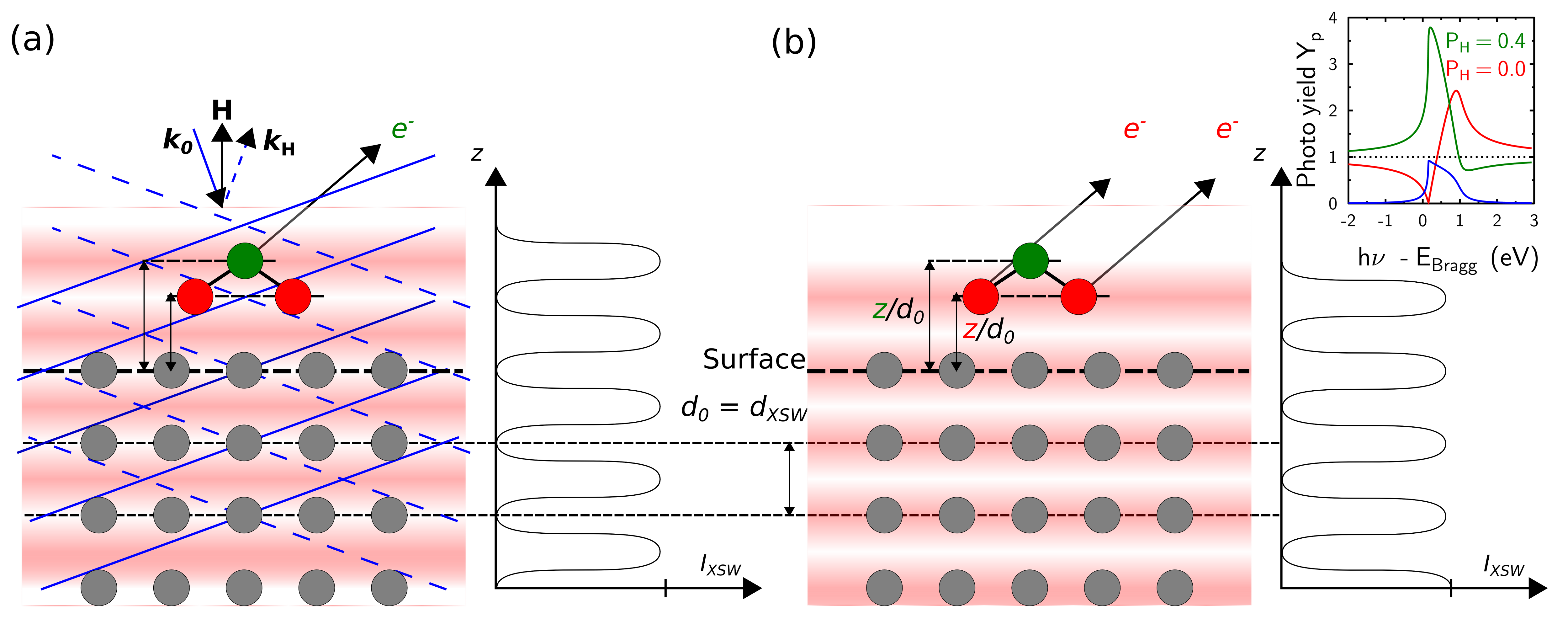
The XSW technique is an interferometric method that exploits the standing wave field created by Bragg diffraction of the incoming X-ray beam. By measuring characteristic photoemission signals, that are related to the local field strength at the position of the excited atomic species, one can derive high-precision and chemically sensitive adsorption distances of molecules on single crystals (see Figure 8 for a schematic).
III.1.1 Concept of XSW measurements
In 1964 Boris W. Batterman first demonstrated that the fluorescence intensity emitted from a single crystal, illuminated with X-rays, changed characteristically when rocking the crystal around the Bragg condition due to the presence of an X-ray standing wave field Batterman_1964_PhysRev. By matching the maxima and minima of the fluorescence signal with the reflected X-ray intensity around the Bragg angle, he correlated them with the relative position of the atomic planes of the crystal. A few years later, he used this concept to locate, within a silicon single crystal, the position of arsenic atoms, used as dopants, relative to the silicon atomic planes Batterman_1969_PhysRevLett. Soon thereafter, it was exploited that the XSW field extends outside the crystal surface Andersen_1976_PhysRevLett, opening up the door to not only the mapping of dopants within a crystal structure Zegenhagen_1993_SurfSciRep; Zegenhagen_2019_JpnJApplPhys and the study of buried interfaces Bedzyk_1988_Science; Lee_1996_PhysicaB; Schneck_2015_CurrOpinColloidInterfaceSci, but also the location of adsorbates on the crystal surface Cowan_1980_PhysRevLett. For the latter, initially, adsorbed atoms were studied Cowan_1980_PhysRevLett; Bedzyk_1985_PhysRevB, Langmuir-Blodgett films Nakagiri_1985_ThinSolidFilms and atomic layers followed Bedzyk_1989_PhysRevLett. Some smaller molecules deposited on different surfaces started to be studied in the 1990s Sugiyama_1995_PhysRevB; Fenter_1998_SurfSci; Shuttleworth_2002_ChemPhysLett; Mulligan_2003_SurfSci, while, the first measurements of conjugated organic molecules on metal surfaces came a few years later Kilian_2002_PhysRevB; Stanzel_2004_SurfSci; Hauschild_2005_PhysRevLett; Gerlach_2005_PhysRevB.
Without entering into the exact mathematical derivation of the XSW field, which is based on dynamical diffraction theory Authier_2003_book, one can explain the basic principle of the XSW technique using the fundamental equation Zegenhagen_1993_SurfSciRep; Woodruff_1998_ProgSurfSci; Vartanyants_2001_RepProgPhys; Gerlach_2013_book; Burker_2014_book; Zegenhagen_2019_JpnJApplPhys
| (1) |
which relates the normalized photo yield from a given chemical species, the intrinsic reflectivity of the crystal and the relative phase between the incoming and the reflected wave with the two structural parameters and . The so-called coherent position , which takes values between 0 and 1 (being both geometrically equivalent), is directly related to the (mean) position of the species being considered via
| (2) |
where introduces an ambiguity that stems from the periodicity of the XSW field of period (cf. Table 1). In most cases, this ambiguity can be removed with common sense and the physical constraints of the system. The index in Eq. (1) and (2) refers to the reciprocal lattice vector of the Bragg reflection employed in the experiment. The coherent fraction is related to the vertical ordering of the species contributing to a given . It assumes values between 0 and 1, with 0 as the outcome of randomly distributed emitters around and 1 the case where all are adsorbing at . Different effects contribute to the decrement of , for instance, thermal vibrations and static disorder. We note that, besides the obvious reason that the adsorption distance only makes sense within the first adsorbed layer of molecules, the significance of the experimental values is limited by . In other words, for a highly disordered layer (), it is pointless to associate any adsorption distance. This has two direct consequences: first, can be used as confidence parameter for the obtained adsorption distance and secondly, coverages below or equal to a full monolayer are desirable to avoid artificially decreasing .
We note that for practical purposes Eq.(1) has to be refined to account, e.g., for the broadening of the reflectivity curve due to the monochromator and the imperfections of the crystals. Also, non-dipole effects in the photoemission process, which affect the angular distribution of the photoelectrons Schreiber_2001_SurfSci; Straaten_2018_JElectronSpectroscRelatPhenom, have to be considered in the data analysis.
III.1.2 Experimental considerations
Generally, datasets for two experimental quantities are required to model the XSW field and subsequently extract the position of a given species relative to the lattice planes of the crystal, i.e. the reflectivity and photo yield when scanning around the Bragg condition . The reflectivity can be measured with a camera directed at a fluorescence screen conveniently located in the chamber and the photo yield is extracted from fluorescence, Auger or photoelectron spectroscopy data from the species of interest: Here, we restrict our discussion to photoelectrons, which are measured through XPS scans performed with different photon energies around (cf. Table 1).
The use of the XSW technique is constrained by rather demanding experimental requirements. Certainly, the first major challenge is the indispensable crystal quality of the substrate, both at the surface as well as in the bulk, which is responsible for the coherence of the standing wave field. In addition to the high photon flux required for these experiments the need to tune the X-ray energy limits the usage of the technique to synchrotron facilities Materlik_1984_PhysLettA. Here, beamlines with insertion devices, crystal monochromators and complex X-ray optics can provide a stable and highly brilliant X-ray beam, that can be (de-)focused to avoid beam damage on the samples. The reader is referred to Refs. Zegenhagen_2010_JElectronSpectroscRelatPhenom; Zegenhagen_2013_book; Lee_2018_SynchrotronRadiatNews for a more detailed explanation of the beamline requirements.
The experimental geometry, namely, the relative direction of the incoming beam with respect to the sample and the electron analyzer is essential. It can be shown that when creating the interference field in back-reflection (see Figure 8), i.e. the incoming and the Bragg-reflected beam being almost perpendicular to the diffracting crystal planes (diffraction angles close to ), the intrinsic angular width of the reflectivity curve is largest. Thereby, the need for nearly perfect crystallinity of the substrates is relaxed Woodruff_1988_SurfSci. XSW experiments performed under these conditions are referred to as normal-incidence (NI)XSW and have become standard for measuring adsorption distances of larger molecules on metals.
Recently, it has been demonstrated that dedicated beamlines such as I09 at Diamond Light Source (UK) Lee_2018_SynchrotronRadiatNews, which is operational since 2013, can implement significant improvements in performance and usability compared to previous installations. Due to the optimized experimental setup and data-acquisition methods the signal-to-background and signal-to-noise ratio of the photoelectron spectra could be improved without risking extensive beam damage even for molecular systems. If the electron analyzer is positioned at an angle of 90∘ with respect to the incident X-ray beam (as realized at I09), the substrate background in the spectra is strongly suppressed and also the non-dipole contributions to the photoelectron yield are minimized. Overall, the challenges associated with XSW measurements have to some degree shifted away from the technical side and more towards the sample preparation and data analysis. Indeed, by using a proper core-level model to account for the different contributions to the photoelectron yield one can extract adsorption distances for the chemically inequivalent species within a molecule. Hence, the systematic combination of XSW experiments with high-resolution XPS allows to resolve intramolecular distortions that were not accessible before and thereby extend the significance of XSW results beyond average adsorption distances Mercurio_2013_PhysRevB; Blowey_2017_FaradayDiscuss; Franco-Canellas_2017_PhysRevMaterials. For that matter, accurate Smith_2016_Carbon and preferably theory-backed core-level models Diller_2017_JChemPhys; Baby_2015_BeilsteinJNanotechnol are necessary.
Over the years, different software packages have been used for handling (NI)XSW data. For fitting the core-level spectra the commercial CasaXPS CASAXPS has become very popular. For the analysis of the resulting photoelectron yield data, on the other hand, there are various specialized tools available. Recently, Bocquet et al. discussed the general formalism and contributed a new open source program with graphical user interface (Torricelli) that facilitates the fitting of XSW data. Bocquet_2019_ComputPhysCommun As also pointed out in Ref. Straaten_2018_JElectronSpectroscRelatPhenom, the analysis can be non-trivial, if the large angular aperture of the analyzer and the finite tilt of the sample are considered. As a concluding remark, we also note that via off-normal XSW measurements, i.e. using a Bragg reflection with a finite in-plane component of H, it is in principle possible to triangulate the position of adsorption sites Cheng_2003_PhysRevLett. Since for large adsorbate molecules this can be difficult Weiss_2017_PhysRevB, our focus is on the vertical structure along the surface normal.
III.2 Photoelectron spectroscopy
Photoelectron spectroscopy (PES) is a well-known and established technique to determine the electronic structure of solids and is described in detail in various books and review articles Egelhoff_1987_SurfSciRep; Cardona_1978_book; Nefedov_1988_book; Hufner_2003_book; Schattke_2008_book; Fadley_2010_JElectronSpectroscRelatPhenom; Bagus_2013_SurfSciRep; Suga_2014_book; Moser_2017_JElectronSpectroscRelatPhenom; Dil_2019_ElectronStruct. In this section we will, thus, deal with issues specific to PES on organic thin films Rao_1979_ApplSpectroscRev; Seki_1986_ChemPhys; Netzer_1992_CritRevSolidStateMaterSci; Cahen_2003_AdvMater; Crispin_2003_JPolymSciB; Crispin_2004_JAmChemSoc; Rocco_2008_JChemPhys; Ueno_2008_ProgSurfSci; Puschnig_2009_Science; Bussolotti_2015_JElectronSpectroscRelatPhenom; Schultz_2017_AdvMaterInterfaces; Munoz_2018_MacromlRapidCommun; Kirchhuebel_2019_PhysChemChemPhys including the main pitfalls and obstacles.
III.2.1 Ultraviolet photoelectron spectroscopy
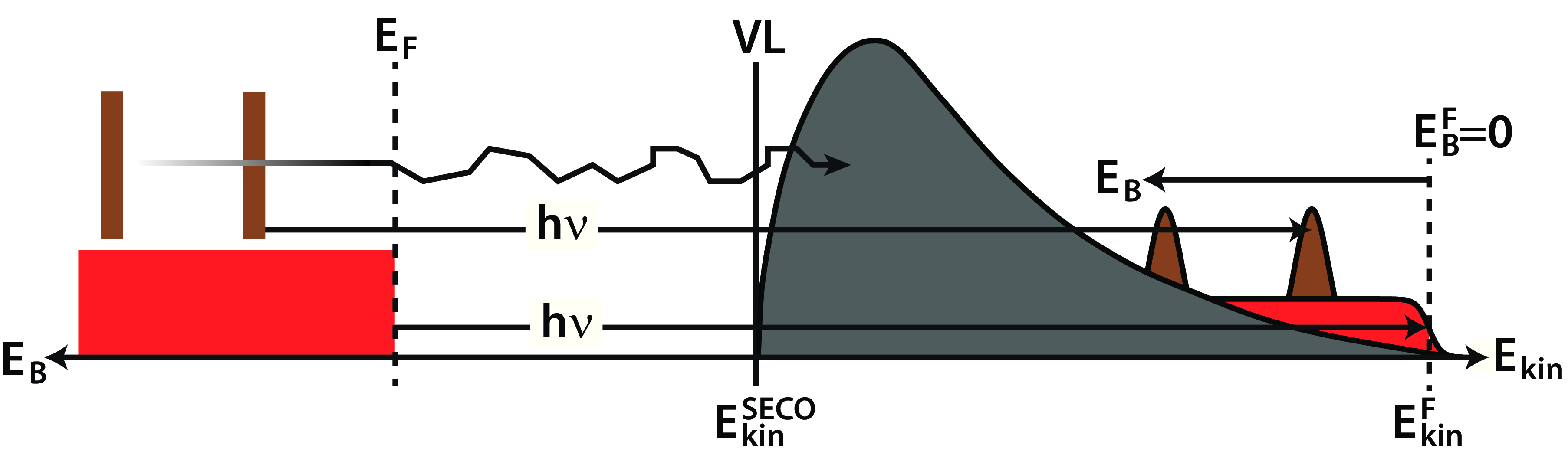
First, we will focus on ultraviolet photoelectron spectroscopy (UPS). Figure 9 displays on the left side two energy-levels (HOMO and HOMO-1) of an organic thin film on a metal substrate, for which the continuous occupied DOS is shown. The sample is irradiated with monochromatic UV-light with photon energy and the resulting photoemission intensity is shown on the right side of Figure 9. An electron analyzer measures the kinetic energy and intensity of photoelectrons. The resulting spectra are usually plotted as function of binding energy with the Fermi level serving as energy reference ( eV). The information depth is limited by the inelastic mean free path of photoelectrons. The so-called “universal curve” gives a value of 7 Å for electrons with a kinetic energy of 15 eV (typical for measurements with He I) in organic materials Seah_1979_SurfInterfaceAnal. Consequently, for (sub)monolayer coverages of a flat lying COM film on a metal, molecular features and substrate features appear concomitantly.
In addition to valence electron features, also secondary electrons (gray in Figure 9) contribute to the spectrum. These electrons have been inelastically scattered in the sample and thus lost the information about their initial state. However, they can be used to determine the VL of the sample, since at a certain kinetic energy () the energy of secondary electrons is not sufficient to overcome the surface potential of the sample. At this energy their intensity is dropping to zero, which is often called secondary-electron cutoff (SECO). The VL of the sample (w.r.t. ) is given by the difference of the photon energy and the whole width of the spectrum, i.e.:
| (3) |
This rather simplified description is sufficient to determine the VL of samples with a homogenous surface potential. However, as mentioned above, the adsorption of COMs usually modifies the work function of clean metal surfaces. For submonolayer coverages, or in the case of island growth, the sample features local surface potentials Wandelt_1997_ApplSurfSci; Koller_2007_OrgElec; Duhm_2009_JElectronSpectroscRelatPhenom; Schultz_2017_AdvMaterInterfaces; Schultz_2019_PhysStatusSolidiB; Wang_2016_SciRep; Tada_2011_NatMater; Siles_2018_Small. Depending on the lateral dimensions of these inhomogeneities, either two separate SECOs can be observed (for large island sizes) or the SECO position is determined by the area-weighted mean of the local surface potentials. A detailed description and guidelines on how to analyze SECOs are given in Ref. Schultz_2019_PhysStatusSolidiB. This publication describes, furthermore, how to determine IEs of organic thin films, which are defined by the SECO and the onset of the HOMO-derived peak Cahen_2003_AdvMater; Kahn_2016_MaterHoriz; Koch_2008_JPhysCondensMatter; Kahn_2003_JPolymSciBPolymPhys; Ishii_1999_AdvMater; Schultz_2019_PhysStatusSolidiB.
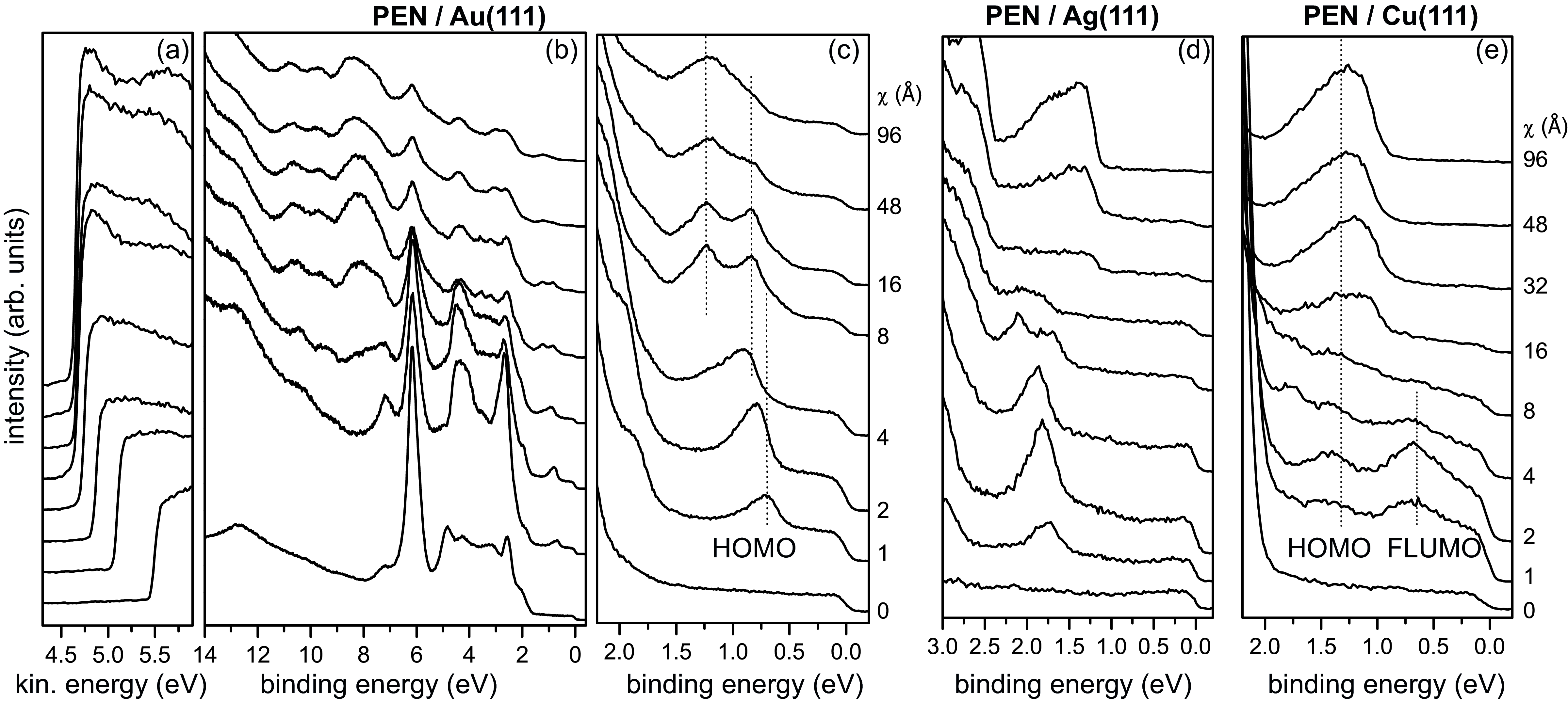
In general, for discussing interfacial interactions often “monolayer” and “multilayer” energy-levels are compared (cf. Figure 5). The thickness of vacuum-sublimed thin films in organic molecular beam deposition (OMBD) is usually measured by a quartz-crystal micro balance and corresponds, thus, to a nominal mass thickness. In that process, layer-by-layer growth is rather the exception than the rule and island or Stranski-Krastanov (island on wetting layer) growth dominates Venables_1984_RepProgPhys; Yang_2015_ChemRev; Winkler_2016_SurfSci; Kowarik_2017JPhysCondensMatter; Schreiber_2004_PhysStatSolA. Thus, the first step in interpreting photoemission data is to identify the spectrum which is most dominated by monolayer contributions. A first hint gives the evolution of the SECO as adsorption induced charge rearrangements often saturate upon monolayer formation. For PEN, which may be regarded as the “fruit fly” of organic surface science Kuroda_1961_CanJChem; Lee_1977_ChemPhysLett; Sebastian_1981_ChemPhys; Moerner_1999_Science; Kang_2003_ApplPhysLett; Eremtchenko_2005_PhysRevB; Fukagawa_2006_PhysRevB; Kafer_2007_PhysRevB; Koch_2007_AdvMater; Zheng_2007_Langmuir; Dougherty2008JPCC; Koch_2008_JAmChemSoc; Yamane_2009_JElectronSpectroscRelatPhenom; Puschnig_2009_Science; Toyoda_2010_JChemPhys; Han_2013_ApplPhysLett_PEN; Duhm_2013_ACSApplMaterInterfaces; Park_2016_AnalChem; Ji_2017_CanJChem; Zhang_2017_AdvElectronMater; Kera_2018_JPhysSocJpn; Choi_2018_NatMater; Hoffmann-Vogel_2018_RepProgPhys; Klues_2018_CrystEngComm; Doring_2019_JPhysCondensMatter; Nakayama_2019_JPhysChemLett; Tadano_2019_PhysRevApplied, thickness-dependent UP spectra on Au(111), Ag(111) and Cu(111) Lu_2016_JPhysCondensMatter are shown in Figure 10 as a typical example of UPS at organic-metal interfaces. Indeed, for PEN on Au(111) the VL (as deduced from the SECO position in Figure 10a) decreases rapidly up to a nominal PEN thickness of 4 Å. However, this does not mean that a nominal thickness of 4 Å corresponds to a closed monolayer. It simply tells that from this thickness on, subsequently deposited molecules grow predominantly in multilayers.
The suppression of substrate features, e.g., the Au -bands in a BE range from 2 to 8 eV in Figure 10b or the Fermi-edge in Figure 10c, with increasing coverage can be used to estimate the growth mode of the adsorbate. However, the applicability of the universal curve to organic thin films has been questioned Bussolotti_2013_PhysRevLett; Graber_2011_SurfSci; Ozawa_2014_JElectronSpectroscRelatPhenom and only qualitative statements are straightforward. For PEN/Au(111) the substrate Fermi-edge is still visible for a nominal coverage of 96 Å, which corresponded to more than twenty layers of flat lying PEN. This clearly shows that the growth mode is not layer-by-layer. For the spectra with a nominal thickness of 96 Å on Ag(111) and Cu(111), on the other hand, the Fermi-edge is (almost) invisible, pointing to less pronounced island growth.
The shape of HOMO-derived UPS peaks is often not simply Gaussian. For well ordered monolayers and sufficient experimental resolution, hole-phonon coupling Koch_2007_AdvMater; Kera_2009_ProgSurfSci; Kera_2015_JElectronSpectroscRelatPhenom becomes evident in UP spectra as can be seen by the high-BE shoulder of the HOMO-derived peak in the spectra for a nominal coverage of 2 Å on Au(111) and Ag(111) (Figures 10c and d). Furthermore, factors like the measurement geometry and the photon energy impact photoemission intensities. For example, the emission from the HOMO of flat-lying -conjugated molecules has typically a maximum for an emission angle of 45∘ and a minimum for normal emission Hollerer_2017_ACSNano; Puschnig_2009_Science; Liu_2014_JElectronSpectroscRelatPhenom; Yagishita_2015_JElectronSpectroscRelatPhenom.
The spectra in Figure 10 are measured with an hemispherical analyzer and angle-integrated over along , which is a typical measurement geometry. Also such angle-integrated spectra can reflect energy dispersing features, in particular if rotational domains related to the substrate symmetry are involved. This explains the HOMO-shape of PEN in multilayers on Ag(111), in which PEN adopts a herringbone arrangement Kafer_2007_ChemPhysLett and exhibits a band dispersion Yoshida_2008_PhysRevB. Notably, also former LUMO derived energy-levels of organic monolayers on metals can show intermolecular energy dispersion Yamane_2013_PhysRevLett; Ules_2014_PhysRevB. For PEN on Au(111) the multilayer growth mode is still under debate Kafer_2007_PhysRevB; Kang_2003_ApplPhysLett and, hence, the multilayer HOMO features have not been unambiguously assigned Lu_2016_JPhysCondensMatter. Overall, great care has to be taken when comparing measurements obtained in different experimental setups. For example, in an early publication of PEN on Cu(111) the former LUMO-derived peak just below the Fermi level (Figure 10e) has been overlooked Koch_2008_JAmChemSoc. Moreover, small differences in, e.g., temperature, substrate cleanness, evaporation rate or impurities, can have a significant impact on organic thin film growth and, consequently, the electronic structure Lee_1977_ChemPhysLett; Schreiber_2004_PhysStatSolA; Salzmann_2007_ApplPhysLett; Witte_2008_PhysStatSolA; Breuer_2011_CrystGrowthDes; Ji_2017_CanJChem; Jones_2016_AdvFunctMater; Cocchi_2018_PhysChemChemPhys.
III.2.2 X-ray photoelectron spectroscopy
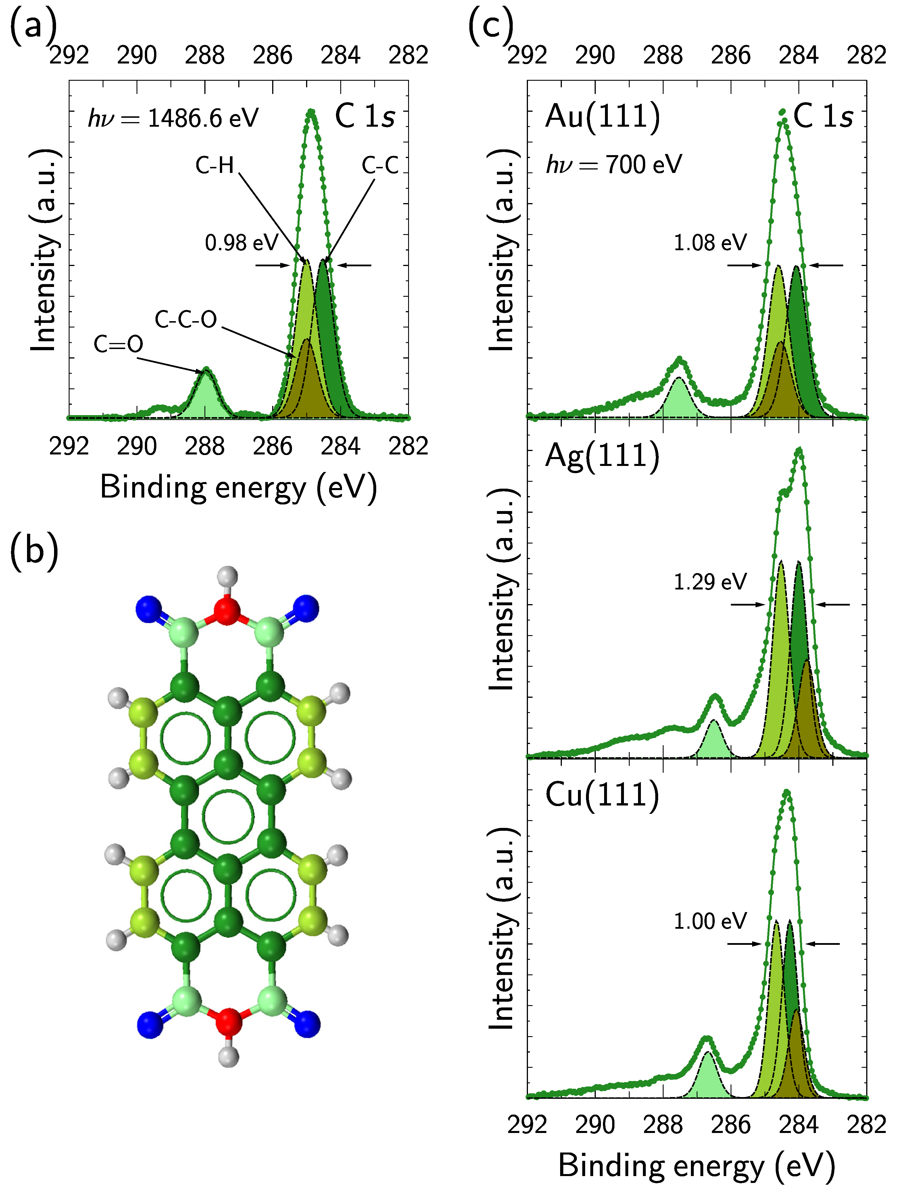
For XPS the electronic structure of the sample is probed with X-rays, whose higher photon energy make core-levels accessible Nefedov_1988_book; Moulder_1995_book; Fadley_2010_JElectronSpectroscRelatPhenom; Crist_2019_JESRP. Core-levels provide information about the local chemical environment of the atoms, which gives rise to so-called chemical shifts in XP spectra Chadwick_1981_JESRP; Travnikova_2012_JElectronSpectroscopRelatPhenom. Figure 11a shows the C 1s spectrum of a PTCDI multilayer on Au(111) Franco-Canellas_2017_PhysRevMaterials illustrating the strong chemical shift between carbon atoms in the functional groups (C=O) and in the perylene backbone. The chemically inequivalent carbon atoms within the molecule can be precisely resolved if the shift in energy is large enough, which is often the case for carbon bound to electronegative atoms (e.g. O and F). The binding-energy (or core-level) shifts associated with the chemical structure can be further modified by the molecular environment, for instance if there are strong intermolecular interactions, and/or by the proximity of the substrate. Intrinsic or extrinsic peak broadening is another complication when describing core-level signals. Its origin is manifold and a proper description often requires electronic structure calculations.
The fine structure of the core-levels can only be resolved using a sufficiently high energy resolution, which is feasible when measuring at synchrotron radiation facilities or with monochromatized lab-sources. Generally, monolayer spectra may include fingerprints of (chemical) interactions with the substrate Freund_1996_SurfSciRep; Crispin_2003_JPolymSciB; Scholl_2004_JChemPhys; Lanzilotto_2018_ChemEurJ. For PTCDI on Au(111) the interaction is weak Franco-Canellas_2017_PhysRevMaterials and therefore the multilayer (Figure 11a) and monolayer (Figure 11c) spectra are – except for a rigid shift due to screening – almost identical. PTCDI monolayers on Ag(111) and Cu(111), however, are chemisorbed Franco-Canellas_2017_PhysRevMaterials, which is reflected in non-rigid shifts of the components attributed to different chemical environments of the multilayer versus the monolayer spectra; in particular, the energetic spacing between the C=O-derived peak and the main peak decreases for the PTCDI monolayer (Figure 11c). In addition to the insight in the chemistry of adsorbates, chemical shifts in XPS facilitate the experimental determination of individual vertical binding distances for each carbon species using the XSW technique (Figure 7).
III.3 Complementary techniques
The XSW technique is mostly applied to the measurement of adsorption distances and molecular distortions perpendicular to the surface. Alternatively, photoelectron diffraction (PhD) Woodruff_2007_SurfSciRep provides a full, local 3D positioning of a given species with respect to the surface atoms Lorenzo_2011_SurfSci; Duncan_2012_JPhysChemC; White_2018_SurfSci. However, while rather successful for certain (preferably simple) systems, the data analysis and interpretation are not straightforward since inequivalent positions may be difficult to decouple, thus challenging its application to larger adsorbates Duncan_2010_SurfSci; Salomon_2015_JPhysChemC. Similarly, LEED I-V may provide a 3D picture of an adsorbate Stellwag_1995_SurfSci; Zheleva_2012_JPhysChemC; Sirtl_2013_PhysChemChemPhys, but the analysis of the data is computationally expensive and requires some initial guess of the adsorbate position. Both, PhD and LEED I-V require a certain degree of registry/commensurability between the adsorbate and the substrate, which limits their use to systems with in-plane order. Surface X-ray diffraction Feidenhansl_1989_SurfSciRep; Robinson_1992_RepProgPhys; Meyerheim_1998_ApplPhysA; Krause_2003_JChemPhys, and specifically the so-called rod scans (along ) for the vertical structure, are slightly less demanding to model (thanks to the applicability of the kinematic, i.e. single-scattering, approximation), but the sensitivity to light elements is limited because of low X-rays scattering cross-sections. Importantly, it is very difficult to obtain element-specific positions needed to determine possible distortions/bending of the adsorbates. In contrast, relative positions, such as tilt angles, can be inferred with NEXAFS by exploiting the geometry-dependent absorption of X-rays without the need of long-range order Stoehr_1992_book; Diller_2012_JChemPhys; Breuer_2015_JElectronSpectroscRelatPhenom. We note that other popular techniques in the study of inorganic surfaces and interfaces such as reflection high-energy electron diffraction (RHEED), scanning-electron microscopy (SEM) or ion scattering-based techniques are not very common in our context because of the probable beam damage induced by the high energy of incoming particles. Some notable exceptions can be found though SchmitzHubsch_1997_PhysRevB.
Although not the focus of this review, a full characterization of the interface geometry involves the in-plane structure of the adsorbed layers and their registry with the surface atoms. Scanning-tunneling microscopy (STM) Rosei_2003_ProgSurfSci; Barth_2007_AnnuRevPhysChem; Han_2012_SurfSciRep; Klappenberger_2014_ProgSurfSci; Wagner_2015_ProgSurfSci; Gottfried_2015_SurfSciRep; Dong_2016_ProgSurfSci; Wakayama_2016_JpnJApplPhys; Bouju_ChemRev_2017; He_2017_ChemPhysChem; Goronzy_2018_ACSNano and low-energy electron diffraction (LEED) Mannsfeld_2006_ModPhysLettB; Hooks_2001_AdvMater; Forker_2017_SoftMatter are the most popular techniques in this context in addition to grazing-incidence X-ray diffraction Feidenhansl_1989_SurfSciRep, which provides the highest resolution. STM offers real-space images with atomic resolution, which can be combined with local spectroscopy measurements. However, any quantitative determination of vertical adsorption structures with STM is still challenging Woodruff_2019JpnJApplPhys. Notably, with atomic force microscopy (AFM) under UHV conditions one can estimate vertical bonding distances, although input from DFT-modeling is necessary to extract absolute numbers Schuler_2013_PhysRevLett. LEED offers reciprocal-space information that is averaged over a large sample area. With more elaborate versions such as LEED I-V, mentioned above, and spot-profile analysis LEED (SPA-LEED) a precise description of the adsorbate unit cell can be achieved Kilian_2004_SurfSci. Finally, low-energy electron microscopy (LEEM) provides in particular real-time information of the in-plane arrangement and morphology during growth Levesque_2016_JPhysChemC; Henneke_2017_NatMater; Felter_2019_Nanoscale.
In Sec. III.2 photoemission spectroscopy was introduced as a tool to study the energy-level alignment and interfacial coupling by using the energy information of photoelectrons. Beyond that, i.e. by exploiting also the momentum information of the electrons Seki_1986_ChemPhys; Ueno_2008_ProgSurfSci; Offenbacher_2015_JElectronSpectroscRelatPhenom; Udhardt_2017_JPhysChemC; Hollerer_2017_ACSNano; Yagishita_2015_JElectronSpectroscRelatPhenom; Liu_2014_JElectronSpectroscRelatPhenom; Puschnig_2009_Science; Bussolotti_2017_NatCommun, new possibilities arise, which – although not within the scope of this article – shall be briefly summarized here. By angle-resolved and photon-energy dependent UPS measurement possible in-plane Ueno_2008_ProgSurfSci; Yamane_2017_JPhysChemLett; Koller_2007_Science; Kakuta_2007_PhysRevLett and out-of-plane Ueno_2008_ProgSurfSci; Aghdassi_2018_Nanotechnology; Yamane_2013_PhysRevLett band dispersions of organic thin films can be accessed. Moreover, even for largely angle-integrated measurements the photoelectron angular distribution (PAD) provides insight into, e.g., the orientation of COMs on the surface Hollerer_2017_ACSNano; Puschnig_2009_Science; Liu_2014_JElectronSpectroscRelatPhenom; Yagishita_2015_JElectronSpectroscRelatPhenom. The vibrational fine structure of HOMO-peaks allows to assess charge reorganization energies and thus to estimate hopping mobilities by a ‘first-principle’ experiment Coropceanu_2002_PhysRevLett; Kera_2009_ProgSurfSci; Perroni_2014_Electronics; He_2016_JPhysChemC; Graus_2016_PhysRevLett. Moreover, the development of instrumentation over the last decades has made it possible to measure photoelectron reciprocal-space maps, often termed “orbital tomography”, which can be used to reconstruct molecular orbitals in real space and/or to precisely assign photoemission intensities to a particular molecular orbital Ules_2014_PhysRevB; Yang_2019_JPhysChemLett Dauth_2014_NewJPhys; Graus_2018_JPhysSocJpn; Hollerer_2017_ACSNano; Puschnig_2009_Science; Egger_2019_NewJPhys.
Two-photon photoemission (2PPE) spectroscopy provides insight into electron dynamics of interface states Ueba_2013_JPhysChemC; Marks_2014_JElectronSpectroscRelatPhenom; Gerbert_2017_JPhysChemC; Yamada_2018_ProgSurfSci; Lerch_2018_JPhysCondensMatter. In conjunction with real-space information, e.g., by LEED or STM, detailed insight in organic-metal coupling is possible Schwalb_2008_PhysRevLett; Zaitsev_2016_PhysRevB; Lerch_2017_JPhysChemC. Accessing the unoccupied density of states by inverse photoemission (IPES) is demanding, as cross-sections and overall energy resolution are notoriously low and, most importantly, beam damage can be a problem for organic thin films Kanai_2009_ApplPhysA; Zahn_2006_ChemPhys; Krause_2013_OrgElec. Some of these issues can be overcome by low-energy inverse photoemission spectroscopy (LEIPS) Yoshida_2015_JElectronSpectroscRelatPhenom; Han_2013_ApplPhysLett_PEN. Scanning tunneling spectroscopy (STS), as a local probe, accesses unoccupied states as well as occupied states close to and can furthermore identify site-specific interactions at organic-metal interfaces Song_2017_ACSNano; Klappenberger_2014_ProgSurfSci; Kraft_2006_PhysRevB; Rohlfing_2007_PhysRevB; Gonzalez-Lakunza_2009_ChemPhysChem; FernandezTorrente_2008_JPhysCondensMatter; Nazin_2003_Science, also measurable with high-resolution electron energy-loss spectroscopy (HREELS) Eremtchenko_2003_Nature; Lu_2009_ChemPhysLett; Navarro_2015_JPhysChemC; Ruckerl_2017_BeilsteinJNanotechnol. With in situ optical differential reflectance spectroscopy (DRS) optical properties can be measured during deposition Forker_2009_PhysChemChemPhys; Forker_2012_AnnuRepProgChemSectCPhysChem; Navarro-Quezada_2015_RevSciInstrum; Nickel_2018_JPhysChemC; Meisel_2018_JPhysChemC.
Temperature-programmed desorption (TPD), with a proper modelling of the data, is used to measure the adsorption energy of a particular adsorbate on a given substrate Redhead_1962_Vacuum; Lord_1974_SurfSci; Chan_1978_ApplicationsofSurfaceScience; Chan_1978_ApplicationsofSurfaceSciencea; Habenschaden_1984_SurfSci; Fichthorn_2002_PhysRevLett; Winkler_2016_SurfSci; Maass_2018_JChemPhys. This parameter is important for a precise and quantitative distinction between adsorption regimes and has become, together with the adsorption distance, a benchmark parameter for state-of-the-art DFT calculations Liu_2015_PhysRevLett; Maurer_2016_ProgSurfSci. Other uses include the study of thermally-activated on-surface reactions Haq_2011_JAmChemSoc; Rockert_2014_ChemEurJ; Chen_2014_JPhysChemC; Ferrighi_2015_ChemEurJ, the assessment of the thin-film growth, desorption kinetics and the thermal stability of a given system Lukas_2001_JChemPhys; Kafer_2009_ApplPhysAMaterSciProcess; Frank_2009_ChemPhysLett; Gotzen_2011_Langmuir; Breuer_2013_JChemPhys; Winkler_2016_SurfSci; Thussing_2017_JPhysChemC. Finally, in-situ IR spectroscopy provides insight into the vibrational modes and changes thereof upon adsorption. It is also useful for identifying unknown sample compositions and may give information on changes in the adsorbate charge Broker_2010_PhysRevLett. Of course, there are also many other spectroscopic techniques including, e.g., Raman and photoluminescence, that can be applied to study some of the isssues discussed here, but rather indirectly and outside the scope of this review.