| DOI: | Electronic structural critique of interesting thermal and optical properties of C17Ge germagraphene. |
| Sujoy Datta,a,b Debnarayan Janaa | |
| DATE: | In this communication, we report a theoretical attempt to understand the involvement of electronic structure in determination of optical and thermal properties of C17Ge germagraphene, a buckled two dimensional material. The structure is found to be a direct bandgap semiconductor with low carrier effective mass. Our study has revealed the effect of spin-orbit coupling on the band structure and in appearance of spin Hall current in the material. A selectively high blue to ultraviolet light absorption and a refractive index comparable to flint glass open up the possible applicability of this material for optical devices. From electronic structural point of view, we investigate the reason behind its moderately high Seebeck coefficient and power factor comparable to traditional thermoelectric materials. Besides its narrow bandgap, relatively smaller work function of C17Ge () than graphene () and germanene () assures more easily removal of electron from the surface. This material is turned out to be an excellent alternative for futuristic semiconductor application from optical to thermal device regime. |
1 Introduction
The discovery of graphene 1 and related compounds revolutionized modern semiconductor industry. Subsequently, other 2D materials like silicene 2, black-phosphorene 3, and borophene 4 were synthesized experimentally.
Though graphene exhibits extraordinary thermal, mechanical and electrical properties, its zero band-gap imposes a severe constraint on its practical applicability. As a result, opening up the band-gap of graphene and other planar zero-gap materials has been considered to be the top-most priority in semiconductor engineering. It has been seen earlier that introducing defects in graphene or graphene-nanotubes has a large influence on their electronic properties 5, 6, 7, 8, 9, 10.
Experimental work on such materials have been prolific. The aim of this communication is to use the latest theoretical approaches, together with what we shall argue to be better modifications, and explain these experimental results. Dependable theoretical predictions will then provide the experimentalist a much better handle in choosing their desired materials out of a plethora of possibilities.
Silicon and Germanium being the same group IV material as Carbon, are always the first choice for doping graphene. Several theoretical studies on silicon doped graphene, i.e., siligraphene 11, 12, 13 have been carried out by varying the relative concentrations of Silicon and Carbon. Siligraphene with showed superior sunlight absorbance 11. Wang et al. found theoretically that siligraphene had wonderful Li-ion storage capacity 14. Dong et al. have reported that the stable siligraphene structure (SiC7) exhibited a direct band-gap and superior light absorbance making it a promising donor material for optical-devices 11.
Theoretically, Ge doping was seen to tune the band-gap 15, 16 but these studies never explored the situation of buckled structure. As Ge is much heavier atom than C, doping with Ge is supposed to result in off-the-plain buckling and it is never easy to dope graphene by such a heavier Ge atom. Very recently Tripathi et al. successfully implanted Ge on graphene 17 and found a buckled structure when a Ge atom replaces a C atom. However, when Ge replaces a C-C bond, it can be accommodated in the plane. Hu et al. found buckled C17Ge to be stable and reported lithium ion absorption in this buckled structure 18. However, for functionalization of the germagraphene, electronic structural study should be done more extensively. Here, in this systematic study, we try to explore the electronic, optical and thermal properties of the germagraphene structure.
2 Computational Details
The basic calculations are carried out in plane wave based techniques used in the Quantum Espresso (QE) code 19, 20. Slab geometry for two dimensional system is simulated by introducing 12 Å vacuum on either side of the sheet. The structure is energetically optimized first using variable cell structural relaxation technique. Projected augmented wave (PAW) basis of the Quantum Espresso (QE) is utilised using Perdew-Burke-Ernzerhof (PBE) exchange-correlation potentials21, 22. Charge-densities and energies for each calculation were converged to 10-7 Ry. with the maximum force of 0.001 Ry./atom. k-point meshes are used and force convergence and pressure thresholds are set as 0.0001 Ry./au and 0.0000 Kbar, respectively. The self consistent field (SCF) calculation on the relaxed structure is done using dense k-point mesh for PBE and k and q point meshes for HSE calculation.
For calculation of spin Hall conductivity (SHC) and transport properties we have used Wannier90 23 package for constructing the maximally localized Wannier functions (MLWF). For construction of MLWF relatively coarse k-ponts as applied in SCF calculation is enough. However, for SHC and transport calculations much dense k-points is needed 24. That is why utilising the Wannier functional way is always beneficial 25. A fine sample of and k-points are used for SHC and thermal property calculations, respectively. Wannier interpolation technique is also applied for the HSE band plotting.
BoltzWann module of Wannier90 is a powerful tool for calculating transport properties of material at moderate computational cost 26. The high accuracy in the Brillouin zone integrals can be achieved through Wannierization. In thermal properties calculations we have used adaptive interband smearing and constant relaxation-time of .
For optical property predictions, we calculate the complex dielectric tensor using random phase approximation (RPA).
| (1) |
Here, is the inter-smearing term tending to zero. Since no excited-state can have infinite lifetime, we have introduced small positive in order to produce an intrinsic broadening to all excited states. The imaginary part of the dielectric function has been calculated first and the real part is found using the Kramers-Kronig relation. Optical-conductivity, refractive index and absorption-coefficients were calculated using real and imaginary parts of dielectric functions.27
| (2) | |||
| (3) | |||
| (4) | |||
| (5) | |||
3 Results and discussion
3.1 Structural Properties:
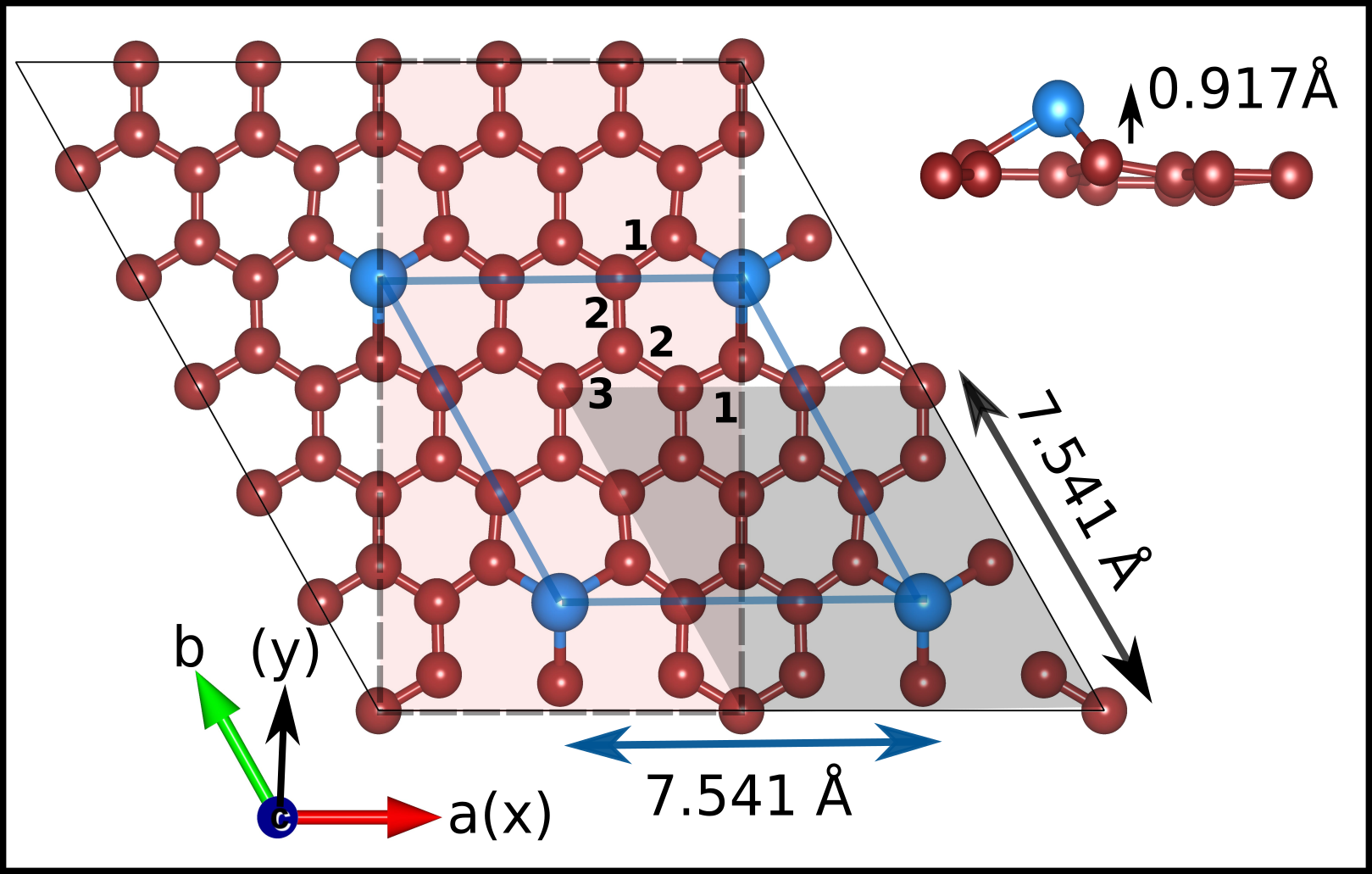
A 33 supercell of graphene (P6/mmm symmetry group) containing 18 C atoms was built. Then a C atom was replaced by Ge and the structure was relaxed. The unit cell of the C17Ge structure is shown as shaded region in Fig. 1.
The geometrically relaxed structure shows buckling. Our calculations complement the experimental finding of buckled germagraphene structure 17 as well as the theoretical result of Hu. et al. 18 who also showed the dynamical stability of the structure. Being a heavier atom, Ge tends to distort the planar graphene structure more than that of siligraphene structures 11. The in-plane lattice constant is 7.541 Å and the Ge atom at 0.917 Å off-the-plane. The separation between layers is kept at 12 Å to nullify the intra-layer interaction, prerequisite for 2D calculations. We can clearly visualize a rhombic formation of Ge atoms connected by blue lines in Fig.1. C-Ge bond length is 1.863 Å, whereas, the C-C bonds denoted by 1, 2, 3 have lengths of 1.411, 1.466, 1.450 Å respectively. So, all the hexagonal rings with only carbon atoms are not regular-hexagons after Ge doping. C-Ge-C, C-C-Ge and C-C-C bond angles are 97.834o, 115.987o and 122.968o, respectively. The buckled structure suggests a deviation from the pure sp2 hybridization which is a signature of planar structure.
Elastic constants:
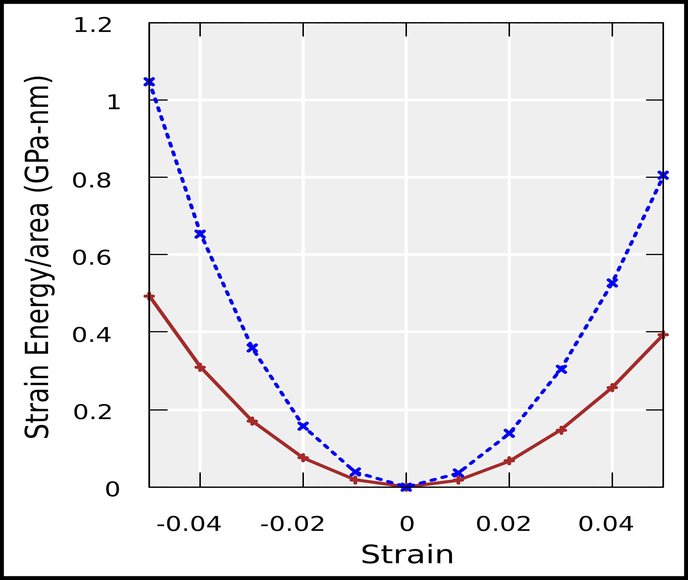
In Fig. 1 the shaded region in pink (dashed line) is used as the cell for the energy of state (EOS) calculation. Uniaxial strain is produced along either in direction (x) or in direction (y). For biaxial stress condition, same percentage of strain is produced along both direction. The total energy is fitted using the equation 28:
| (6) |
where, is the the strain energy per unit area of two dimensional structure. In standard Vigot notation and are the uniaxial in plane strain and is the sheering strain. As the structure is symmetrical along x and y, so, .
In Fig.2 the EOS plot is depicted. The elastic constants are found from the fitting curve as GPa-nm and GPa-nm. These satisfy the Born criteria for mechanical stability of 2D materials, . The in plane Young’s modulus as derived from the formula is 353.949 GPa-nm which is higher than that of graphene (335 GPa-nm) 29 and about three times of MoS2 (123 GPa-nm) 30. The Poission’s ratio defined as is 0.043.
3.2 Electronic Properties:
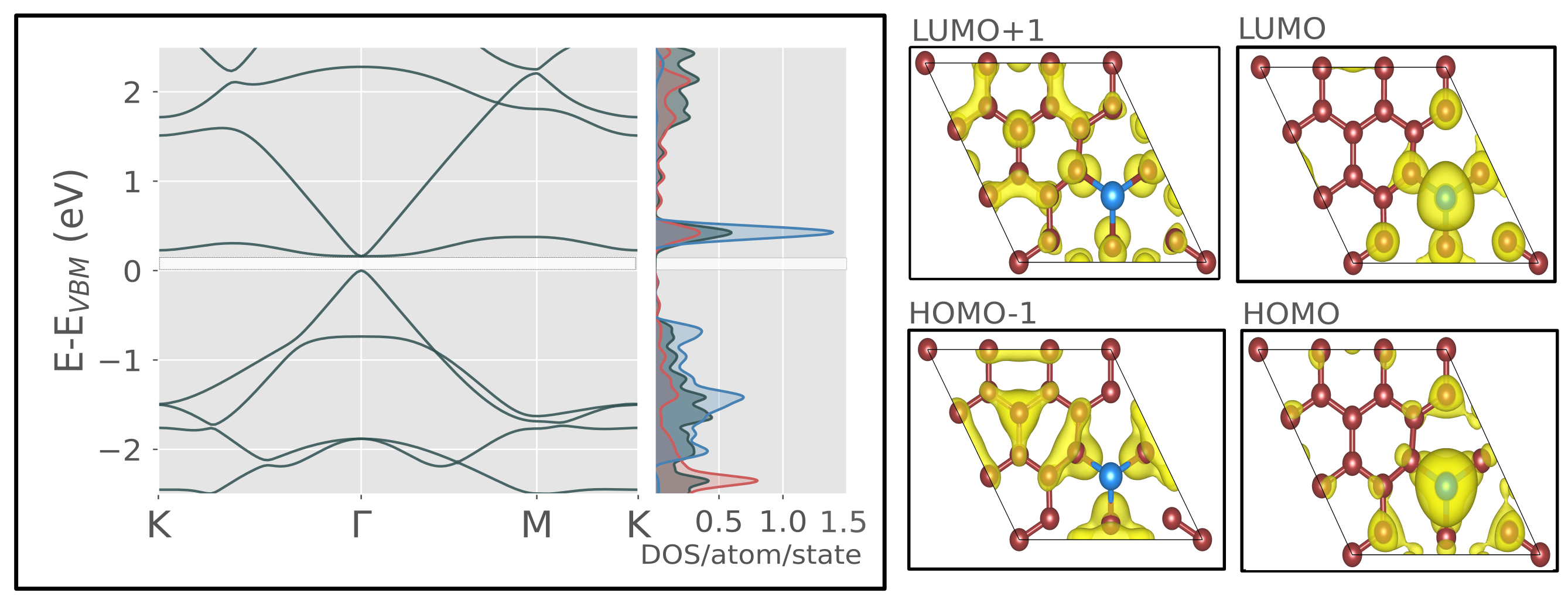
The band structure and densities of states (DOS) for C17Ge are plotted in Fig.3 . The valence band maxima (VBM) is taken as the reference zero of energy axis. From band structure plot it is evident that C17Ge is a direct band-gap semiconductor. The estimated band-gap using PBE is at point.
Near the Fermi energy (EF), there is one band approaching from below, the highest occupied (HO) band. In conduction band region, there are two lower lying bands, one is almost flat, the lowest unoccupied (LU) and another is sharp dipping (LU+1). In the vicinity of , HO and LU bands show almost linear dispersion if moved along to as well as along to . So, similar E-k relation is found for these two bands, both along and , where and are the reciprocal lattice vectors in plane for hexagonal system. Such dispersion isotropy is also present in LU but with much smaller curvature which will affect in the mobility of carriers. However, the dispersive nature of HO and LU bands along and paths are not the same. A HO and HO crossover is seen at about the midway of . At there is a band degeneracy in conduction band as LU and LU bands overlap.
The total density of state (DOS/atom/state) is plotted in grey. Approaching EF from the occupied states below, the total DOS (TDOS) shows a gradual fall, whereas, there is a sharp peak at the lowest unoccupied state. To understand the origin of the bands, we plot the pz projected DOS (pDOS) of C and Ge in red and blue, respectively. The mixing of Ge and C states are evident from pDOS plots. The sharp pDOS peaks of both Ge and C just near CBM suggests the dominant existence of Ge-pz state in LU. The flatness of LU has given rise to this sharp peak, i.e., higher density of states. In valence band (VB) region, the Ge energy states are more available near the EF than at lower energy. Except the sharp peak in LU, the C pDOS rises gradually in both higher and lower energy direction with respect to EF. So, leaving the peak, this nature is a reflection of linear dispersive systems, small DOS around EF. This nature of carbon pDOS and the dominant existence of Ge states in the vicinity of Fermi energy, both in CB and VB confirm the role of Ge in opening the gap between the HO and LU.
The logical conclusion on the origin of the bands near Fermi energy finds a stronger base from the charge density plots in Fig. 3. We have plotted the charge densities for HO, LU as well as HO and LU states. These plots are helpful to identify active sites in C17Ge. The HO and LU states dominated by Ge- states whereas, HO and LU states are composed of C-Ge bonding states with smaller contribution from Ge. As none of the HO, HO, LU, LU sates are localized, the efficiency of photo-absorption is expected. The prevalent existence of Ge- charge densities in HO and LU reassert the role of Ge in band-gap opening.
Carrier Mobility:
Due to the degeneracy of bands at CBM, one flat and a sharp band, it would be interesting to calculate the carrier mobility. Mobility is the defining factor of the dynamical activity of the charge careers in any semiconductor. Higher mobility means speedy charge transfer and low energy loss, yielding better performance and durability of an electronic device.
Mobility is inversely proportional to the effective mass (m∗) of carrier hole or electron. From the band-structure, can be calculated as near the band-edges, for electron at CBM and at VBM for hole.
The calculated hole effective mass is where is electron rest mass. The electron effective mass has two different values due to the band degeneracy at CBM (at ). The electron effective mass originating from LU, is less than that of for the LU band, . Such low light-electron and hole effective mass indicate very high carrier mobility in germagraphene, which is much higher than many 2D materials and reported so far31.
As we find C17Ge as a narrow gap semiconductor, so, its applicability should be compared with the range of II-VI narrow gap semiconductors. For example, both the light-electron and hole effective masses of this germagraphene are almost to those of HgCdTe () 32. So, C17Ge readily can be considered as a better option for the optoelectronic devices like infrared detector, photovoltaic devices etc., those now built by alloying semimetals with II-VI semiconductors 33.
Effect of Intrinsic Spin-Orbit Coupling:
For those systems where space inversion symmetry holds, time reversal symmetry would produce double degeneracy of the bands. Graphene, like many other two-dimensional (2D) materials, preserves inversion symmetry. So, even in the presence of intrinsic spin-orbit coupling (SOC), the Bloch states remain doubly spin degenerate at where the Dirac point originally formed, however, a gap opens up 34. Application of transverse external electric field can lift the spin degeneracy by the Rashba effect. Adatoms having stronger spin-orbit coupling can be doped to open up the band-gap of graphene 35. The system we are dealing here can be otherwise viewed as a periodically doped graphene and having a band gap as well, even in the absence of SOC. So, in presence of intrinsic SOC it is interesting to explore the band structure of C17Ge.
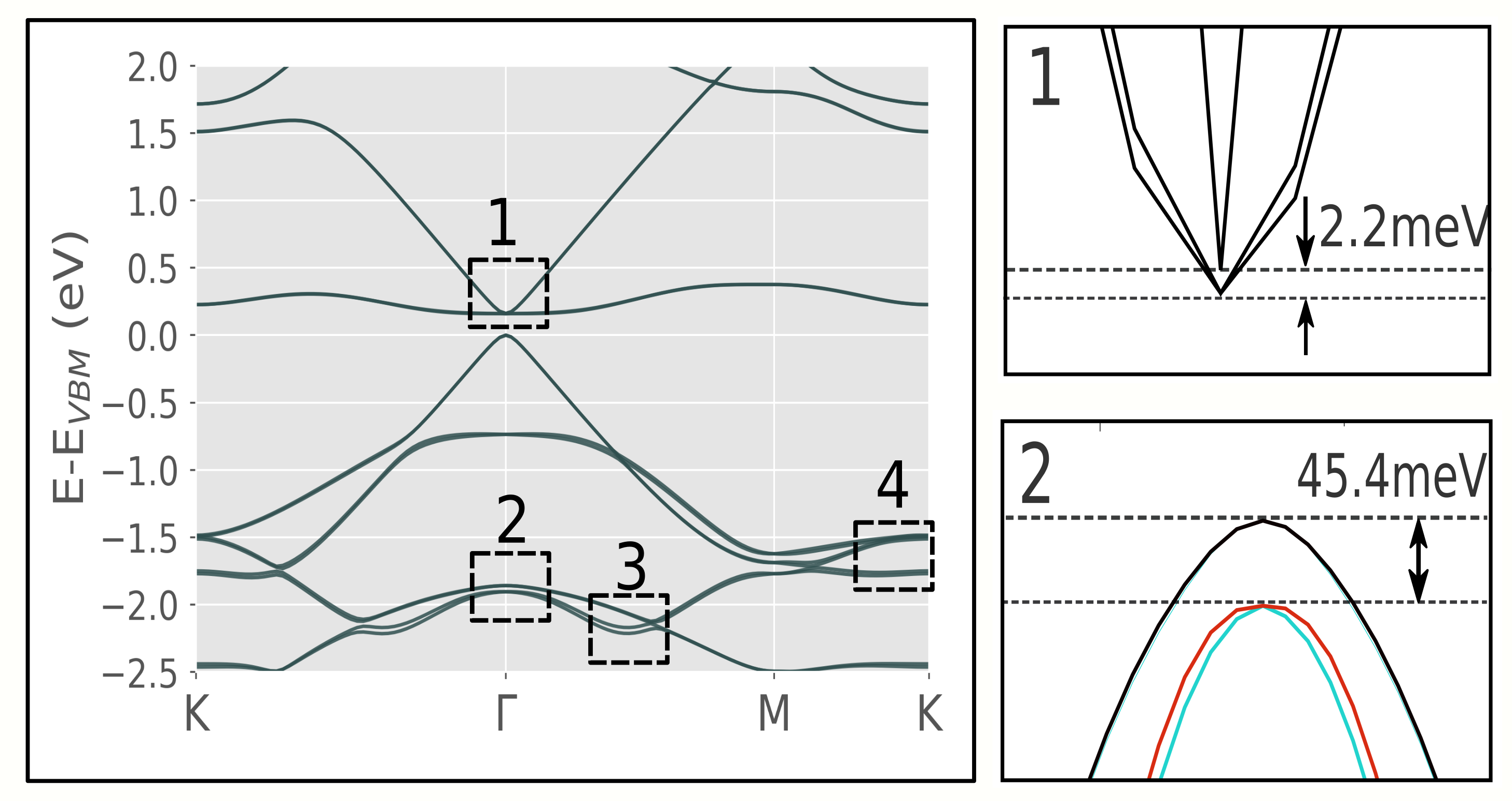
Band structure of C17Ge in presence of intrinsic SOC is shown in Fig.4. Though the plot looks almost same as that without SOC (Fig.3), a close look at several region reveals the difference as represented in the insets. The point, being the centre of reciprocal space, is the most symmetrical point preserving both time reversal and inversion symmetries. So, no spin-orbit spiting is expected at and the regions denoted by 1 and 2 endorse that. However, the band degeneracy of LU and LU is now removed at point by a small value of (Fig.4-1). This has an effect on the effective mass of electron as removal of band degeneracy now confirms this value .
The HO band has considerable C and Ge state mixing and as Ge atom is much heavier than C, spin-orbit coupling effect should be more evident in that band. In the vicinity of point, the splitting is observable and at the Brilouin zone edge the splitting is as large as (Fig.4-4). The degenerate bands in occupied region, below , are now separated by as shown in sub-figure (2).
It was never expected that this C17Ge structure would display large SOC effect, still, the band structure exhibits ample SOC footprint in removing band degeneracies. The spin degeneracy removal, however small it be, can generate spin Hall current in devices and we focus on that in the next section.
Spin Hall Effect:
Intrinsic SOC is an interesting feature of materials as it generates an electric field within such substance, even in absence of any external perturbation. Due to the removal of band degeneracy in intrinsic spin-orbit coupled materials, this transverse electric field triggers spin current. This phenomena is known as spin Hall effect. For different semiconductors and metals this feature is prolific 36. The ab-initio calculations have produced excellent results but these type of direct calculations are excessively expensive as almost number of k-pints are needed for simple semiconducting systems like Ge, GaAs, etc. 24. So, for larger systems with lesser symmetries direct ab-initio calculations become almost impossible. Qiao et al. successfully found an alternative way of calculation through Wannier interpolation and could reproduce the ab-initio results effectively 25 and further applied on layered materials 37.
In presence of electric field along direction, the response of spin () current along the direction can be calculated using linear response theory and the Kubo formula for spin Hall conductivity (SHC) tensor is given by:
| (7) |
where, is the volume of the unit cell, is the number of k-points in Brilouin zone and is the Berry curvature like term expressed as:
| (8) |
The term in curly bracket is coming from the spin current, and is the velocity operator. The matrix elements associated with these two quantities are calculated using Wannier interpolation techniques 23. In dc-SHC calculation, setting blows up the term in Eq.8. To avoid that inter-band smearing has been introduced through an adaptive technique 25, 38.
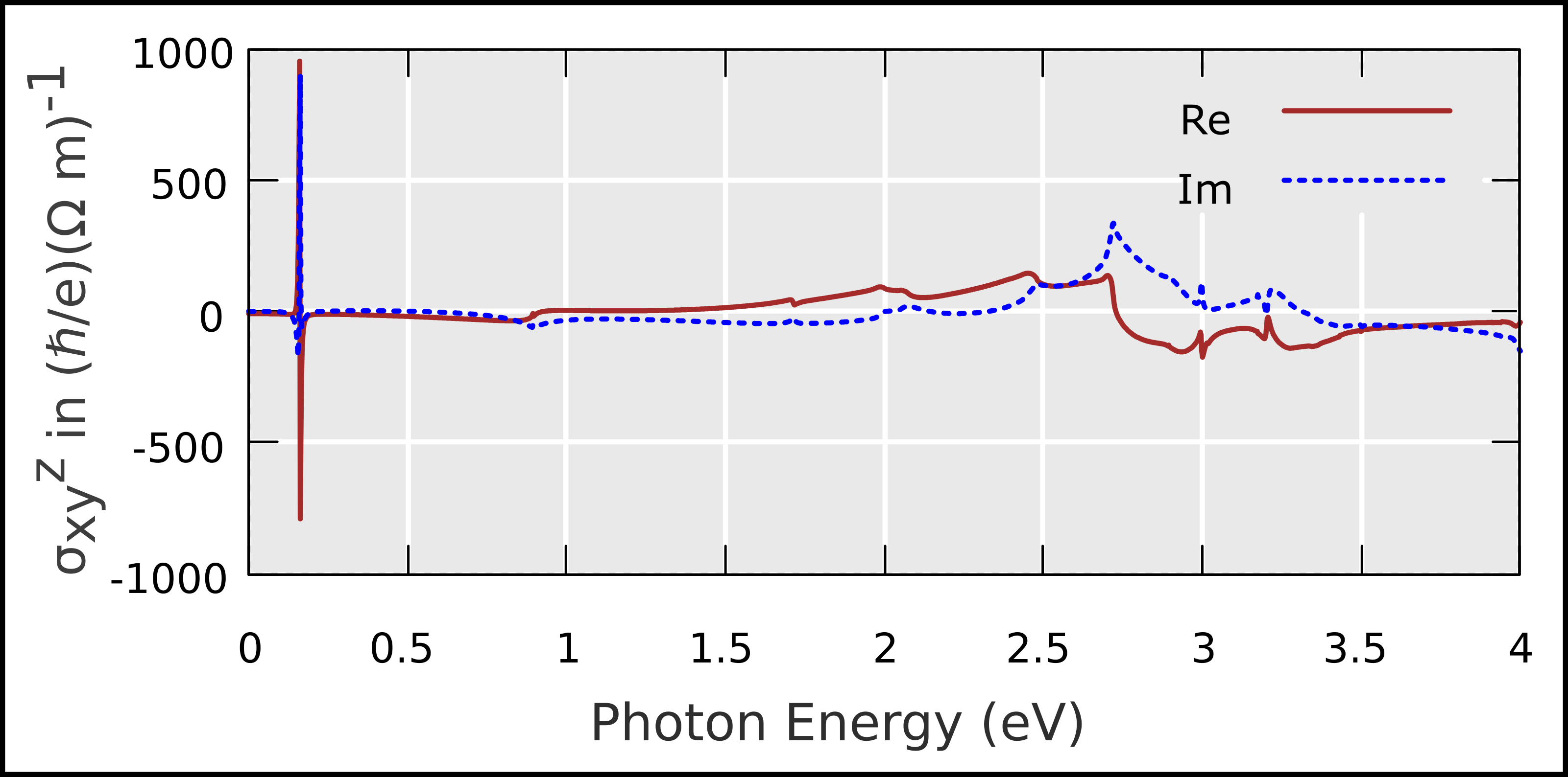
For two dimensional systems, only two components of Hall conductivity tensor is important, and . For symmetrical systems, like we are dealing here, . Though for dc-SHC, the imaginary part is always zero, for ac-SHC a variation of both real and imaginary parts of is expected.
In Fig. 5, we have plotted the variation of real and imaginary parts of ac spin Hall conductivity as a function of energy. As , which is obvious for systems with band gap. The real part of SHC approaches a constant value of for zero energy, whereas, the imaginary part tends to zero. A sharp peak is located around the bandgap value and after that they are almost flat till . Then there are random variations though not much sign change is observed. The real part changes sign where a small peak of imaginary part appears. This peak is not as sharp as observed at . The highest value of is and is . These values are not as large as metallic or semimetallic systems 37, where SOC effect is much prominent. The C- and Ge- electrons are not expected to exhibit large spin Hall effect, however, this result is interesting enough to establish the effect of small doping of same group material in pristine graphene by displaying measurable SHC.
3.3 Optical Properties:
Optical properties of materials are directly related to their electronic structure. While for metallic systems both inter-band and intra-band transitions play role in optical properties, in semiconductors the optical property is mostly governed by inter-band jump. The absorption of a photon by any semiconducting system leads to the transition of an electron from VB to CB. So, the minimum amount of energy required to form the charge carriers should be greater than or equal to its band-gap. The absorption of a photon with energy similar to the bandgap produces a hole in the valence band and an electron in the conduction band. Photons with energy greater than bandgap initiates transition to higher level of conduction band. So, for optical property calculations always plenty of empty bands in CB are taken into consideration. In VB region, the number of electrons participating in the inter-band transitions can be calculated using the expression of effective electron number (neff) given as:
| (9) |
Here, m, e and N are electron mass, charge and density. A saturation of the with photon energy reflects the unavailability of electrons lower than that value for production of hole by jump towards CB. Our calculated value has shown that electrons lying below from VBM is not contributing in the optical transitions. So, all the plots are focused in the range.
In Fig.6, we have depicted the real and imaginary parts of diagonal element of dielectric tensor and electron energy loss spectrum (EELS) as a function of energy. There are two significantly different polarization of electric fields to be considered, one is parallel to the plane of the 2D material (denoted by ) and perpendicular to that plane (denoted by ). The two orthogonal directions (say, x and y) in the plane are symmetric, so, .
Both the real and imaginary parts of parallel dielectric constants show rapid fluctuations in lower energy region. In addition, changes sign four times in this energy region. becomes almost flat only at high energy region ().
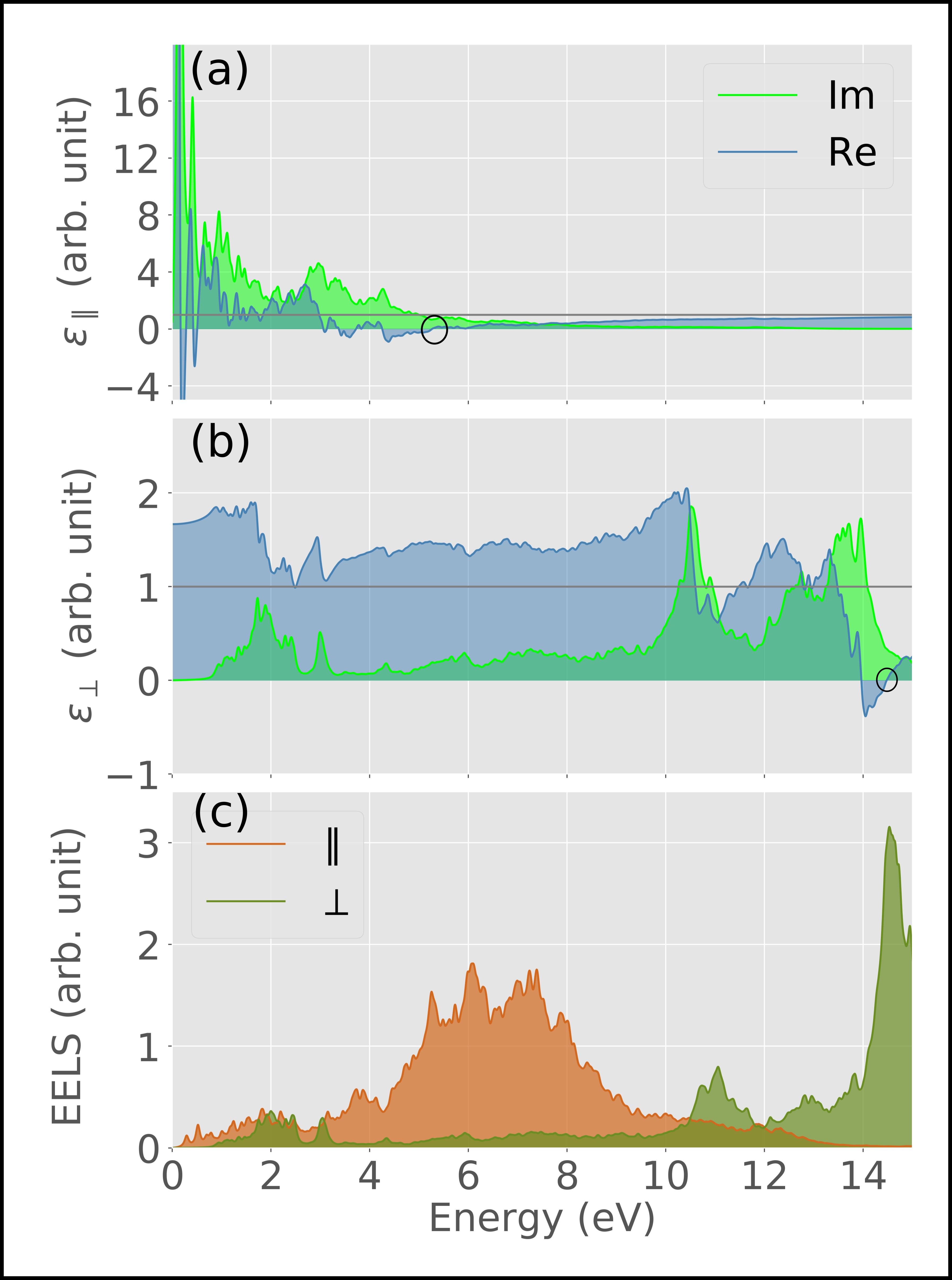
The real part of dielectric constant crosses the zero axis from negative to positive at five different energies, two below and three in the range. The plasma frequency is defined as the frequency when shows positive slope while crossing the zero axis and . The fourth zero crossing energy satisfies both the conditions and identified as the plasma frequency (encircled in Fig.6) for parallelly polarized electric field. This can be readily verified by the peak in EELS. In most of the semiconductors the plasma frequency lies deep into ultraviolet region and germagraphene is not an exception.
We find relatively flat than its perpendicular counterpart. The values are smaller as well. The imaginary part shows a sharp peak around . Unlike , becomes negative to positive only once, at which is the plasma frequency for perpendicular polarization.
Electron energy loss spectrum (EELS) is a properties which can be verified through experiments. In Fig.6(c) the plot of EELS is presented. While the EELS for parallel polarization takes a bell shape centring around , the perpendicular counterpart exhibit significant growth only after . There is a crossover of these two at and thereafter, the perpendicular part is dominant. The sharp peak of EELS⟂ is at the corresponding plasma frequency as found from dielectric constant plot.
Absorption coefficient, refractive index and optical conductivity:
Transition of electron from VB to CB is a result of absorption of photonic energy. So, absorption coefficient preserves the signature of not only band gap but also the full characteristics of bands. Near the Fermi energy, such correspondence can be readily established.
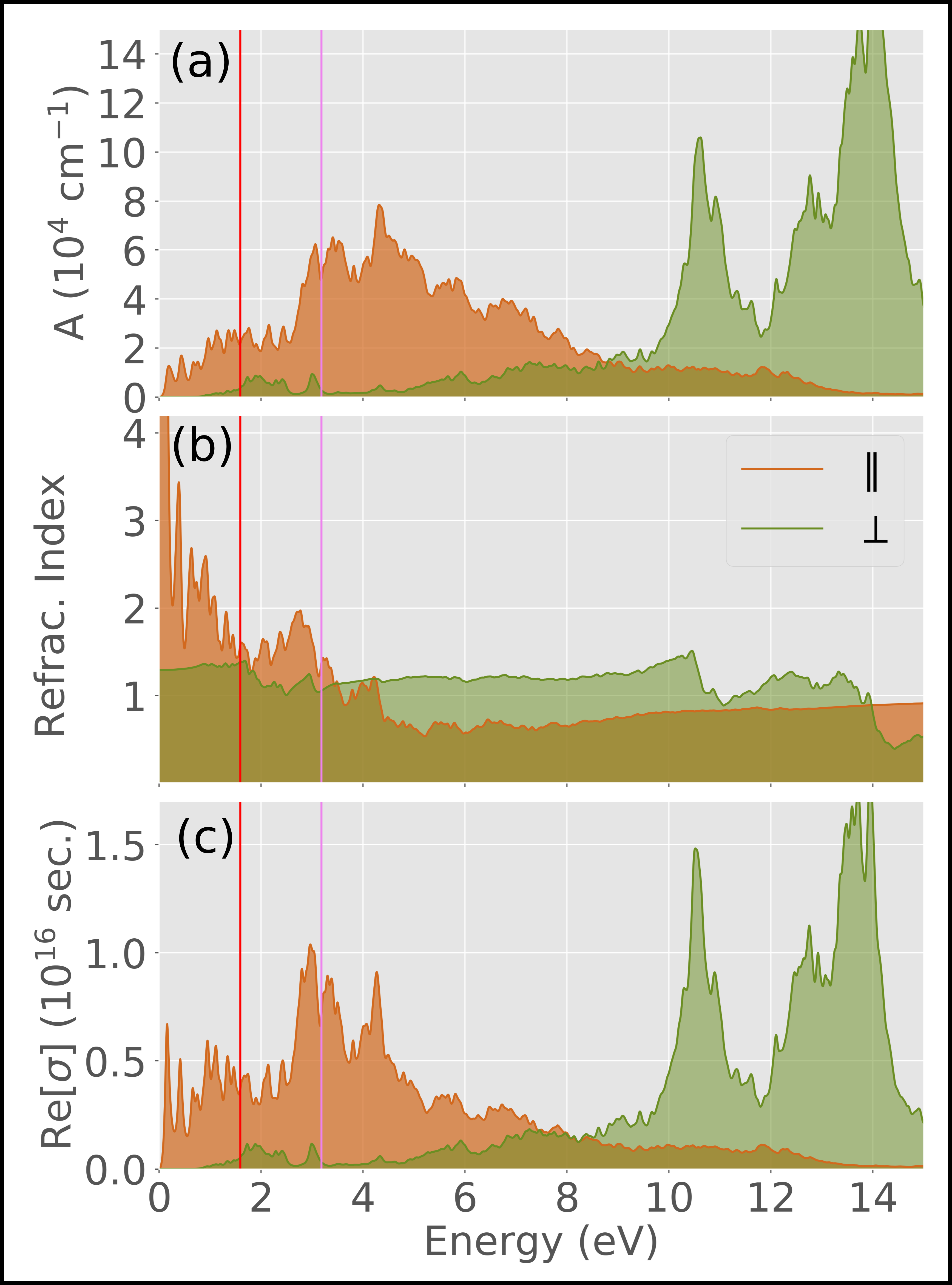
In Fig. 7(a) (b), we plot absorption coefficient as a function of photon energy. To study the one to one correspondence between the electronic structure and photonic absorption we have to look back to Fig.3. The very first small peak in the absorption coefficient (A) for parallel polarization is at corresponds to the band gap of the material. The second peak is between VBM and the small hump of LU band in direction, the third peak around is between the flat region of HO around and CBM. In visible region, the absorption coefficient is showing a gradual increase first, then at around starts to rise stiffly. The jump from around to is attributed from HO to LU transitions as well as from the HO to LU transitions around the midway of and path. This region corresponds to blue-violet colour region. Blue to ultraviolet light absorption is particularly useful for safety of different optical devices through coating by those high absorbing materials.
The absorption coefficient for perpendicular polarization () is negligible with respect to the parallel counterpart till . After that it is dominant as observed for dielectric constant.
In the application for coating on devices another important optical property is the refractive index. The real refractive index of germagraphene structure is depicted as function of photon energy in Fig. 7(b). In the visible range (), the refractive index for parallel polarized electric field varies from to having an average . For comparison, we quote the refractive index of flint glass as , so, this germagraphene material has similar average refractive index to glass for parallel electric field. For perpendicular field, the variation is in range.
There is a direct connection of optical absorption spectra with the imaginary part of the refractive index through the Eq.5. Therefore, the nature of refractive index plots are expected to replicate the peaks and valleys of absorption spectra.
The optical conductivity in Fig. 7(c) shows similar character to absorption coefficient which is logically evident. As more electrons move to CB through photon absorption, the carrier concentration increases resulting in higher optical conductivity. The signature of semiconductors, a gap at the beginning of optical conductivity is clearly visible. The first peak is around the band-gap value of . The peak is sharper than that of the absorption coefficient because the absorption of one photon creates two carriers, one electron and one hole.
3.4 Thermal Properties:
In materials electrons carry both charge and heat. The temperature gradient of any material produces an electric field which opposes the natural diffusion of electrons. So, the electronic conductivity becomes dependent on temperature. The opposing electric field produces the so called Seebeck voltage. The Seebeck coefficient and electronic conductivity depends on this Seebeck voltage. As a gradient dependent quantity, the Seebeck voltage is directly correlated with the grade of asymmetry of electronic distribution around Fermi energy.
A narrow band gap is one of the primary requirement to identify thermoelectric materials for further extensive study, high carrier mobility (low effective mass) is another. Low bandgap helps to pump electrons for conduction even with the help of small thermal excitation with tendency of increasing the electrical conductivity. Besides, direct nature of gap is an additive benefit. Further, low effective mass ensures the high mobility of the carriers, thus, increases the electrical conductivity. However, the decisive factors for searching a promising thermoelectric material consist of a variety of different interconnected properties. From electronic point of view, electrical conductivity (), Seebeck coefficient (S) or the power factor () are the key parameters to dictate the thermoelectric performance.
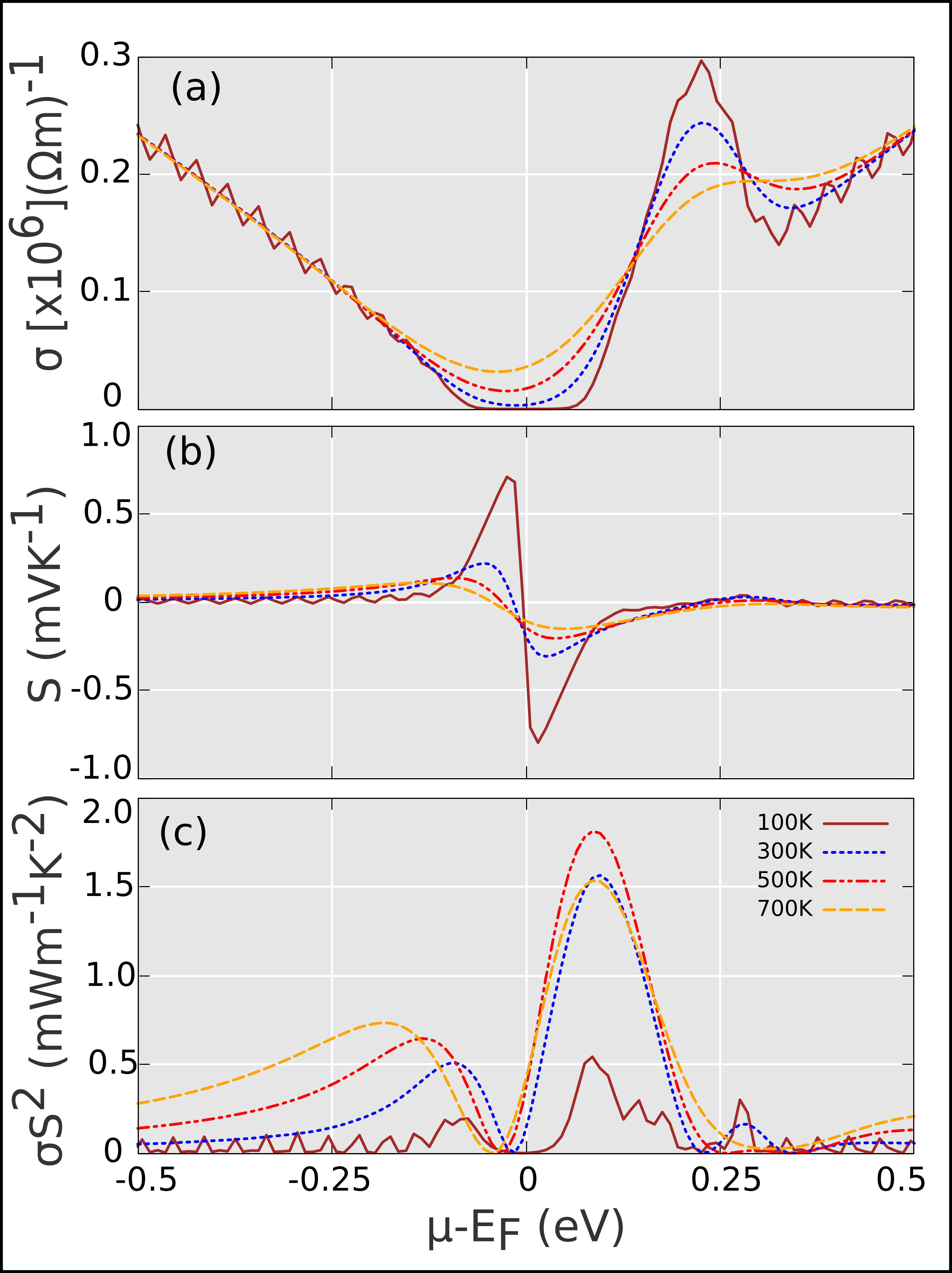
In Fig.8 we have plotted electrical conductivity, Seebeck coefficient and power factor at different temperature (100, 300, 500, 700 K) for C17Ge as functions of chemical potential () as measured from . The zero of chemical potential represents the pristine condition and positive (negative) value indicates the electron (hole) doping. In pristine condition, the conductivity rises with temperature which is a sign of the semiconducting nature of C17Ge.
We have seen in Fig.3 that the DOS has much higher peak around CBM than around VBM. This means more electron concentration in CB edge than hole concentration at VB edge. Hence, asymmetric plot about the zero chemical potential is justified and more electrical conductivity at n-side is a result of higher carrier concentration near CBM.
The electrical conductivity for has sharper variations with comparison to the other temperature plots. Conductivity at room temperature () rises gradually, attains its highest value at and then shows a dip at before staring to rise again. Similar variation is seen for , however at this dip is absent.
At room temperature (300 K) the highest value of Seebeck coefficient is at for n-type doping and at for p-type doping. These values are much higher than the value for pristine graphene, graphene based heterostructure 39, 40, and comparable to Bi2Te3 41. A comparison with other thermoelectric materials is presented in Table. 1 42, 43, 41. High Seebeck effect can be mapped with the rapid variance of DOS. High energy gradient of DOS () is always beneficial for thermoelectric performance44. Under doping, if the Fermi level moves to high DOS peak region, a large asymmetry of thermoelectric power is developed between the hot electrons of energy higher than and cold electrons of energy below Fermi level. Higher anisotropy means higher S, as we can verify for our sample, where the sharp peaks in CB (near CBM) is responsible for highest peaks in Seebeck coefficients. Lower anisotropy of DOS in VB is the reason of lower peak values in region than . As temperature rises, the increase in Joule heating brings down the value of Seebeck coefficient. So, in the figure, we see less Seebeck coefficient for higher temperature.
The power factor of any material is defined as . To understand the electronic structural effect on power factor we have to look back to the carrier effective masses. Higher effective mass is favourable for Seebeck coefficient, whereas it has a negative effect on electrical conductivity. In PF, the second order dependence on S overwhelms the unfavourable effect on . C17Ge has an unusual semiconductor with a very flat LU and very sharp HO band. This in turn initiates the large anisotropy between hole and electron effective masses. So, the power factor follows that anisotropy and for positive the PF peaks are significantly higher than negative . Even the peak for outplays the peak of for n-type doping. For , higher temperature possesses higher maxima.
The power factor at is maximum () near due to significant increase of the electrical conductivity at the high electron doping range. The value of power factor is in between two orthodox thermoelectric materials, Bi2Te3 and Sb2Te3 41, 43 and better than some other proposed materials 45, 46. Moreover, the excellent value of S establishes germagraphene as a potential candidate for thermoelectric application.
| Effective Mass () | |||||||
| Material | Hole | Electron | Seebeck Coefficient () | Power Factor () | Work Function (eV) | ||
| C17Ge | -0.00292 |
|
309 | 1.56 | 4.361 | ||
| Graphene | – | – | 31 39 | 4.390 | |||
| Germanene | – | – | – | – | 4.682 | ||
| GeAs242 | -0.20 | 0.15 | 400 | 0.55 | – | ||
| MoS2 47 | -0.56 | 0.55 | 500-550 48 | 8.5049 | 6.32 | ||
| WSe2 47 | -0.42 | 0.46 | 450-500 48 | 3.20 50 | 5.60 | ||
| Bi2Te3 51 | -0.024 | 0.178 | 323.0 | 2.6041 | – | ||
| Sb2Te351 | -0.054 | 0.045 | 115.6 | 1.00 43 | 4.30 | ||
3.5 Work function:
The work-function () of any material is defined as the energy required to remove an electron from the surface of the material. The highest energy of electron in material is its Fermi energy (), and the energy at the point just outside the surface is originally the vacuum energy (). Work function is the difference of these two:
| (10) |
In intrinsic semiconductors is the mid point energy of VBM and CBM, so, in absolute scale, the orientation of the bands can be found accordingly.
It is well-known that the PBE functional is not adequate enough to determine the work function correctly, whereas, HeydScuseriaErnzerhof (HSE) 52, 53 screened hybrid functional has shown great success for semiconductors. The failure of Local Density Approximation (LDA) and the PBE based Generalized Gradient Approximation (PBE-GGA) in determining the band gap exactly is also evident 54. HSE functional can solve that problem in most of the cases.
We have done the HSE calculation for the same optimized germagraphene unit cell and same energy and charge density cut-off. The k and q point grids are taken as and Optimized Norm-Conserving Vanderbilt (ONCV) pseudopotentials are used. The HSE calculated band-gap is which is higher than PBE calculated value ().
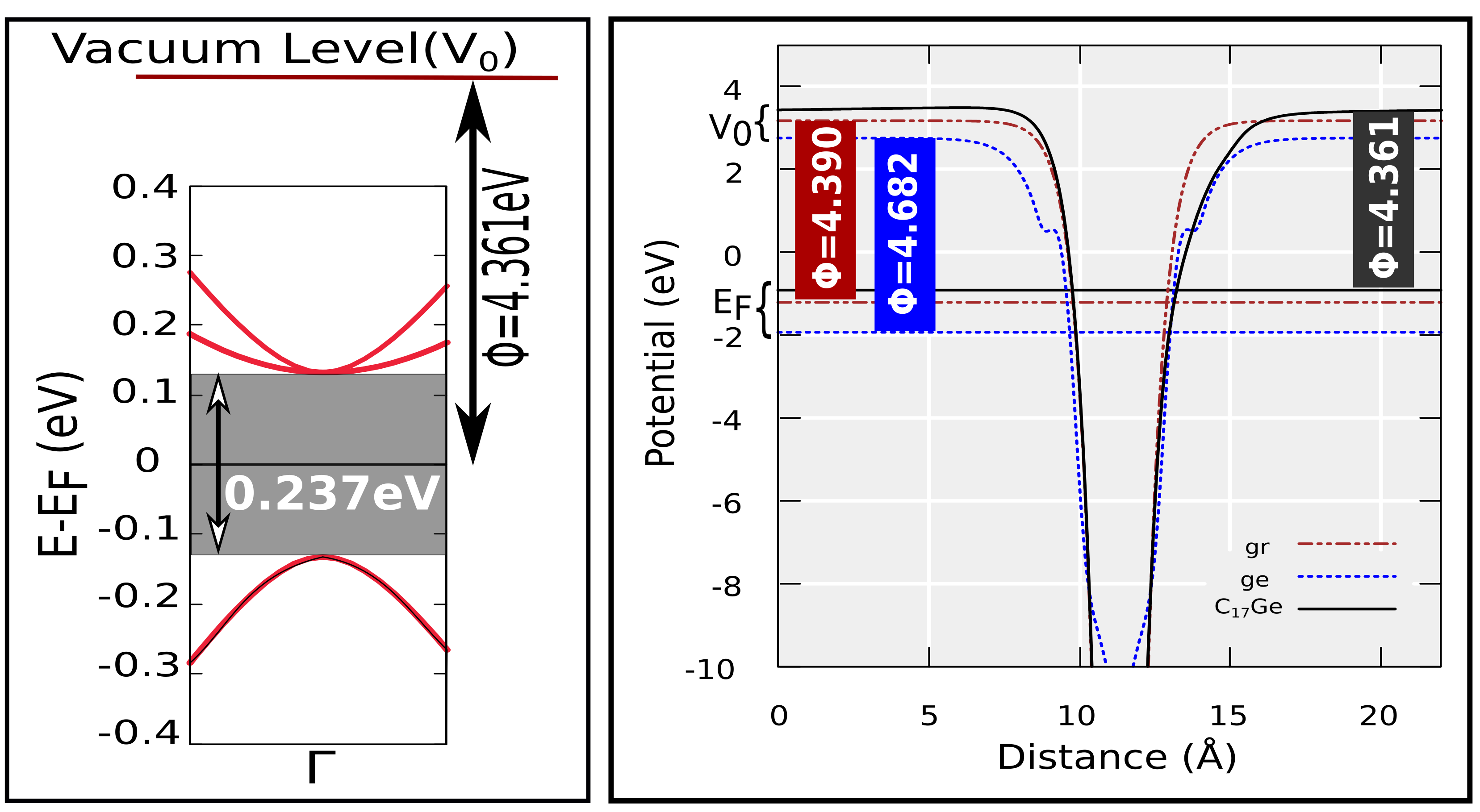
In Fig.9 we plot the electrostatic potentials of germagraphene in comparison with graphene and germanene. The vacuum level is different for different systems and dependent on the software packages, so, for comparison this vacuum level is always standardized to the zero energy. Using Eq.10 the work functions of these three materials are calculated. Our predicted value of graphene monolayer () 55 is at par with experimental result 56 and better than the PBE estimated value 57. The of germanene is similar to the already reported value of 58. The HSE calculated work function of C17Ge is which is lower than both of these. Lower work function is beneficial for removal of electron from material surface. The is of particular interest in the field of photo-catalytic devices through heterojunction formation. Being a material of lower work function than graphene, it may be considered as an alternative to those heterojunction devices where graphene is used now.
4 Conclusion
We show that the stable buckled C17Ge structure is a direct band gap semiconductor having a PBE calculated band gap of . The band degeneracy at the conduction band minima is left when spin orbit coupling is considered. This spin dependent electronic property leaves its footprint on spin hall conduction with highest value of conductivity as . Though this value is not large but effective enough to showcase the effect of anisotropy induced by Ge on the spin dependent electronic property. We also find an exceptionally small hole and light-electron effective mass. These are preferable for optoelectronic devices like infrared detector, photovoltaic devices etc. where high mobility is a perquisite criteria.
The optical and thermal properties of C17Ge are also been explored. This material has exhibited significant blue to ultraviolet light absorption. So, we predict if devices are coated by this material then they can avoid the harm from lower UV region. The refractive index comparable to flint glass is an additional advantage of this material in optoelectronic world.
The narrow band gap of germagraphene makes it a potential candidate for thermoelectric applications. C17Ge has shown relatively larger value of Seebeck coefficient and power factor comparable to traditional thermoelectric materials such as Bi2Te3 and Sb2Te3 at room temperature. Thus, C17Ge affirms brilliant thermoelectric performance. In a sum up, we can conclude that the efficiency of germagraphene in futuristic applications is quite promising.
Acknowledgement
The authors acknowledge the contribution of Late Prof. Abhijit Mookerjee in forming the problem at the initial stage. SD wants to thank Dr. Prashant Singh of Ames Lab., USA and Dr. Chhanda Basu Chaudhuri of Lady Brabourne College, India for their suggestions.
Notes and references
- Novoselov et al. 2004 K. S. Novoselov, A. K. Geim, S. V. Morozov, D. Jiang, Y. Zhang, S. V. Dubonos, I. V. Grigorieva and A. A. Firsov, science, 2004, 306, 666–669.
- Aufray et al. 2010 B. Aufray, A. Kara, S. Vizzini, H. Oughaddou, C. Léandri, B. Ealet and G. Le Lay, Applied Physics Letters, 2010, 96, 183102.
- Liu et al. 2014 H. Liu, A. T. Neal, Z. Zhu, Z. Luo, X. Xu, D. Tománek and P. D. Ye, ACS nano, 2014, 8, 4033–4041.
- Mannix et al. 2015 A. J. Mannix, X.-F. Zhou, B. Kiraly, J. D. Wood, D. Alducin, B. D. Myers, X. Liu, B. L. Fisher, U. Santiago, J. R. Guest et al., Science, 2015, 350, 1513–1516.
- Rao et al. 2014 C. Rao, K. Gopalakrishnan and A. Govindaraj, Nano Today, 2014, 9, 324–343.
- Nath et al. 2014 P. Nath, S. Chowdhury, D. Sanyal and D. Jana, Carbon, 2014, 73, 275–282.
- Das et al. 2016 B. K. Das, D. Sen and K. Chattopadhyay, Physical Chemistry Chemical Physics, 2016, 18, 2949–2958.
- Lee et al. 2014 W. J. Lee, U. N. Maiti, J. M. Lee, J. Lim, T. H. Han and S. O. Kim, Chemical Communications, 2014, 50, 6818–6830.
- Jana et al. 2013 D. Jana, C.-L. Sun, L.-C. Chen and K.-H. Chen, Progress in Materials Science, 2013, 58, 565–635.
- Datta et al. 2017 S. Datta, B. Sadhukhan, C. B. Chaudhuri, S. Chakrabarty and A. Mookerjee, Indian Journal of Physics, 2017, 91, 269–276.
- Dong et al. 2016 H. Dong, L. Zhou, T. Frauenheim, T. Hou, S.-T. Lee and Y. Li, Nanoscale, 2016, 8, 6994–6999.
- Li et al. 2010 Y. Li, F. Li, Z. Zhou and Z. Chen, Journal of the American Chemical Society, 2010, 133, 900–908.
- Li et al. 2014 P. Li, R. Zhou and X. C. Zeng, Nanoscale, 2014, 6, 11685–11691.
- Wang et al. 2018 H. Wang, M. Wu, X. Lei, Z. Tian, B. Xu, K. Huang and C. Ouyang, Nano energy, 2018, 49, 67–76.
- Denis 2014 P. A. Denis, ChemPhysChem, 2014, 15, 3994–4000.
- Kaplan et al. 2013 D. Kaplan, V. Swaminathan, G. Recine, R. Balu and S. Karna, Journal of Applied Physics, 2013, 113, 183701.
- Tripathi et al. 2018 M. Tripathi, A. Markevich, R. Böttger, S. Facsko, E. Besley, J. Kotakoski and T. Susi, ACS nano, 2018, 12, 4641–4647.
- Hu et al. 2019 J. Hu, C. Ouyang, S. A. Yang and H. Y. Yang, Nanoscale Horizons, 2019, 4, 457–463.
- Giannozzi et al. 2009 P. Giannozzi, S. Baroni, N. Bonini, M. Calandra, R. Car, C. Cavazzoni, D. Ceresoli, G. L. Chiarotti, M. Cococcioni, I. Dabo, A. D. Corso, S. de Gironcoli, S. Fabris, G. Fratesi, R. Gebauer, U. Gerstmann, C. Gougoussis, A. Kokalj, M. Lazzeri, L. Martin-Samos, N. Marzari, F. Mauri, R. Mazzarello, S. Paolini, A. Pasquarello, L. Paulatto, C. Sbraccia, S. Scandolo, G. Sclauzero, A. P. Seitsonen, A. Smogunov, P. Umari and R. M. Wentzcovitch, Journal of Physics: Condensed Matter, 2009, 21, 395502.
- Giannozzi et al. 2017 P. Giannozzi, O. Andreussi, T. Brumme, O. Bunau, M. B. Nardelli, M. Calandra, R. Car, C. Cavazzoni, D. Ceresoli, M. Cococcioni, N. Colonna, I. Carnimeo, A. D. Corso, S. de Gironcoli, P. Delugas, R. A. DiStasio, A. Ferretti, A. Floris, G. Fratesi, G. Fugallo, R. Gebauer, U. Gerstmann, F. Giustino, T. Gorni, J. Jia, M. Kawamura, H.-Y. Ko, A. Kokalj, E. Küçükbenli, M. Lazzeri, M. Marsili, N. Marzari, F. Mauri, N. L. Nguyen, H.-V. Nguyen, A. O. de-la Roza, L. Paulatto, S. Poncé, D. Rocca, R. Sabatini, B. Santra, M. Schlipf, A. P. Seitsonen, A. Smogunov, I. Timrov, T. Thonhauser, P. Umari, N. Vast, X. Wu and S. Baroni, Journal of Physics: Condensed Matter, 2017, 29, 465901.
- Perdew et al. 1996 J. P. Perdew, K. Burke and M. Ernzerhof, Physical Review Letters, 1996, 77, 3865–3868.
- Perdew et al. 1997 J. P. Perdew, K. Burke and M. Ernzerhof, Phys. Rev. Lett., 1997, 78, 1396–1396.
- Pizzi et al. 2019 G. Pizzi, V. Vitale, R. Arita, S. Blügel, F. Freimuth, G. Géranton, M. Gibertini, D. Gresch, C. Johnson, T. Koretsune et al., Journal of Physics: Condensed Matter, 2019.
- Guo et al. 2005 G. Y. Guo, Y. Yao and Q. Niu, Phys. Rev. Lett., 2005, 94, 226601.
- Qiao et al. 2018 J. Qiao, J. Zhou, Z. Yuan and W. Zhao, Physical Review B, 2018, 98, 214402.
- Pizzi et al. 2014 G. Pizzi, D. Volja, B. Kozinsky, M. Fornari and N. Marzari, Computer Physics Communications, 2014, 185, 422–429.
- Wooten 2013 F. Wooten, Optical properties of solids, Academic press, 2013.
- Liu et al. 2018 X. Liu, X. Shao, B. Yang and M. Zhao, Nanoscale, 2018, 10, 2108–2114.
- Şahin et al. 2009 H. Şahin, S. Cahangirov, M. Topsakal, E. Bekaroglu, E. Akturk, R. T. Senger and S. Ciraci, Physical Review B, 2009, 80, 155453.
- Yue et al. 2012 Q. Yue, J. Kang, Z. Shao, X. Zhang, S. Chang, G. Wang, S. Qin and J. Li, Physics Letters A, 2012, 376, 1166–1170.
- Miró et al. 2014 P. Miró, M. Audiffred and T. Heine, Chemical Society Reviews, 2014, 43, 6537–6554.
- Rogalski 2005 A. Rogalski, Reports on Progress in Physics, 2005, 68, 2267.
- Baker 2007 I. Baker, Springer handbook of electronic and photonic materials, 2007, 855–885.
- Han et al. 2014 W. Han, R. K. Kawakami, M. Gmitra and J. Fabian, Nature nanotechnology, 2014, 9, 794.
- Weeks et al. 2011 C. Weeks, J. Hu, J. Alicea, M. Franz and R. Wu, Physical Review X, 2011, 1, 021001.
- Sinova et al. 2004 J. Sinova, D. Culcer, Q. Niu, N. Sinitsyn, T. Jungwirth and A. H. MacDonald, Physical Review Letters, 2004, 92, 126603.
- Zhou et al. 2019 J. Zhou, J. Qiao, A. Bournel and W. Zhao, Physical Review B, 2019, 99, 060408.
- Yates et al. 2007 J. R. Yates, X. Wang, D. Vanderbilt and I. Souza, Phys. Rev. B, 2007, 75, 195121.
- Reshak et al. 2014 A. Reshak, S. A. Khan and S. Auluck, Journal of Materials Chemistry C, 2014, 2, 2346–2352.
- Duan et al. 2016 J. Duan, X. Wang, X. Lai, G. Li, K. Watanabe, T. Taniguchi, M. Zebarjadi and E. Y. Andrei, Proceedings of the National Academy of Sciences, 2016, 113, 14272–14276.
- Cheng et al. 2014 L. Cheng, H. Liu, J. Zhang, J. Wei, J. Liang, J. Shi and X. Tang, Physical Review B, 2014, 90, 085118.
- Wang et al. 2017 F. Q. Wang, Y. Guo, Q. Wang, Y. Kawazoe and P. Jena, Chemistry of Materials, 2017, 29, 9300–9307.
- Lee et al. 2015 M. H. Lee, K.-R. Kim, J.-S. Rhyee, S.-D. Park and G. J. Snyder, Journal of Materials Chemistry C, 2015, 3, 10494–10499.
- Wu et al. 2018 J. Wu, Y. Chen, J. Wu and K. Hippalgaonkar, Advanced Electronic Materials, 2018, 4, 1800248.
- Wang et al. 2012 D. Wang, W. Shi, J. Chen, J. Xi and Z. Shuai, Physical Chemistry Chemical Physics, 2012, 14, 16505–16520.
- Guilmeau et al. 2015 E. Guilmeau, A. Maignan, C. Wan and K. Koumoto, Physical Chemistry Chemical Physics, 2015, 17, 24541–24555.
- Rasmussen and Thygesen 2015 F. A. Rasmussen and K. S. Thygesen, The Journal of Physical Chemistry C, 2015, 119, 13169–13183.
- Ghosh and Singisetti 2015 K. Ghosh and U. Singisetti, Journal of Applied Physics, 2015, 118, 135711.
- Hippalgaonkar et al. 2017 K. Hippalgaonkar, Y. Wang, Y. Ye, D. Y. Qiu, H. Zhu, Y. Wang, J. Moore, S. G. Louie and X. Zhang, Physical Review B, 2017, 95, 115407.
- Yoshida et al. 2016 M. Yoshida, T. Iizuka, Y. Saito, M. Onga, R. Suzuki, Y. Zhang, Y. Iwasa and S. Shimizu, Nano letters, 2016, 16, 2061–2065.
- Yavorsky et al. 2011 B. Y. Yavorsky, N. Hinsche, I. Mertig and P. Zahn, Physical Review B, 2011, 84, 165208.
- Heyd and Scuseria 2004 J. Heyd and G. E. Scuseria, The Journal of chemical physics, 2004, 121, 1187–1192.
- Heyd et al. 2005 J. Heyd, J. E. Peralta, G. E. Scuseria and R. L. Martin, The Journal of chemical physics, 2005, 123, 174101.
- Perdew et al. 1982 J. P. Perdew, R. G. Parr, M. Levy and J. L. Balduz Jr, Physical Review Letters, 1982, 49, 1691.
- 55 S. Datta, P. Singh, D. Jana, C. B. Chaudhuri, M. K. Harbola, D. D. Johnson and A. Mookerjee, To be published, arXiv preprint arXiv:1908.06596.
- Yan et al. 2012 R. Yan, Q. Zhang, W. Li, I. Calizo, T. Shen, C. A. Richter, A. R. Hight-Walker, X. Liang, A. Seabaugh, D. Jena et al., Applied Physics Letters, 2012, 101, 022105.
- Ziegler et al. 2011 D. Ziegler, P. Gava, J. Güttinger, F. Molitor, L. Wirtz, M. Lazzeri, A. Saitta, A. Stemmer, F. Mauri and C. Stampfer, Physical Review B, 2011, 83, 235434.
- Li et al. 2016 P. Li, J. Cao and Z.-X. Guo, Journal of Materials Chemistry C, 2016, 4, 1736–1740.