Design of micron-long superconducting nanowire perfect absorber
for efficient high speed single-photon detection
Abstract
Despite very efficient superconducting nanowire single-photon detectors (SNSPDs) reported recently, combining their other performance advantages such as high speed and ultra-low timing jitter in a single device still remains challenging. In this work, we present a perfect absorber model and corresponding detector design based on a micron-long NbN nanowire integrated with a 2D-photonic crystal cavity of ultra-small mode volume, which promises simultaneous achievement of near-unity absorption, gigahertz counting rates and broadband optical response with a 3 dB bandwidth of 71 nm. Compared to previous stand-alone meandered and waveguide-integrated SNSPDs, this perfect absorber design addresses the trade space in size, efficiency, speed and bandwidth for realizing large on-chip single-photon detector arrays.
I. Introduction
Superconducting nanowire single-photon detectors (SNSPDs)1, 2 are recognized as one of the most important photon detection technologies in quantum information processing and communications3, 4, 5, due to their high internal quantum efficiency over a broad wavelength band6, 7, 8, 9, 10, 11, fast speed12, 13, excellent timing performance14, 15, 16 and ultra-low dark count rates17, 18. However, these individual performance characteristics have been so far best optimized in separate device designs, and it still remains a challenge to incorporate all the high performance merits in a single device, due to the inherent trade-off between detection efficiency and bandwidth over a desired nanowire length. For example, in most high-efficiency SNSPD designs, it is preferable that the devices consist of an ultra-thin and millimeter-long superconducting nanowire meandered into a circular shape with > diameter to guarantee near-unity coupling efficiency from fiber to detector6, 7, 8, 19, which renders the detectors subject to speed limited by the large kinetic inductance of the long nanowires20. Integrating the nanowire detectors with on-chip optical waveguides could greatly increase the interaction time of the nanowire with photons and thereby reduce the absorption length of the nanowire down to tens of micrometers21, 22, 23, 24, 25, 26, 27, 28, 29, 30, 31. Nevertheless, the total length of the nanowire needs further scale down below in order to realize gigahertz counting rates32. Moreover, the SNSPD with a record-low timing jitter below is only demonstrated with a -long NbN nanowire recently 14 in order to suppress the geometry-induced jitter33, albeit with a compromised detection efficiency due to direct fiber illumination. Considerable efforts have been devoted to further reducing the nanowire length by embedding the nanowires into a variety of cavities, such as 1D-, 2D-photonic crystal (PhC) cavities34, 32, 12 and racetrack ring resonators35. While as short as -long nanowires are demonstrated with a considerable absorption, the use of resonant cavities introduces spectral selectivity, resulting in an operation bandwidth of only several nanometers.
The main goal of this work is to design a near-perfect absorber for an ultra-short nanowire of a micron length while simultaneously maintaining a broad operation bandwidth around the telecommunication wavelength of 1550 nm. We begin by theoretically studying a general one-side cavity model in Section II to guide the optimization of the nanowire loaded cavity system. Then, we systematically investigate the absorption rates of the waveguide-integrated NbN nanowires in dependence on the index contrast of waveguides, nanowire geometry and varying waveguide types to maximize the photon loss per round-tip in the cavity (Section III). In Section IV, we present the design and simulation results of the ultra-short NbN nanowire integrated with an H0-type 2D-PhC cavity, which demonstrates an ultra-small mode volume and thus enables the nanowire to achieve a near-unity peak absorption efficiency combined with more than 3 dB bandwidth maintained. In Section V, we compare our design with previous implementations of SNSPDs based on different device structures, and the results demonstrate orders of magnitude improvement achieved with our design in terms of the bandwidth-nanowire-length ratio, which holds promise for realizing a large array of high-performance on-chip single-photon detectors for future integrated quantum photonic circuits.
II. One-side cavity model
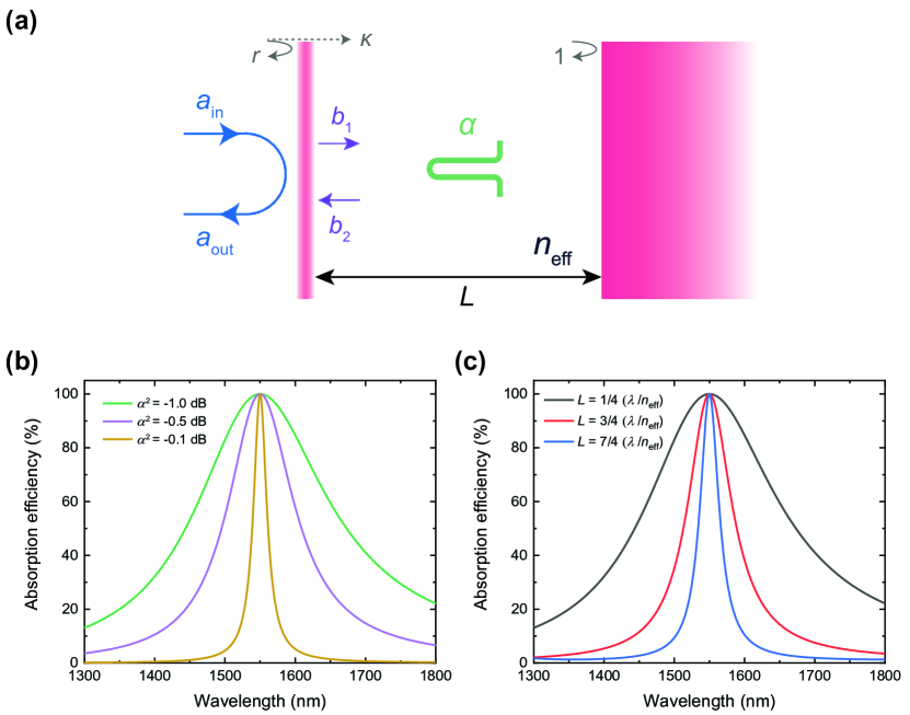
In order to study the effect of the cavity on the nanowire absorption bandwidth, we propose a simple and general one-side cavity model as illustrated in Fig. 1(a). The nanowire is placed inside a cavity which is formed by a full reflective mirror combined with another partial reflective mirror. Through the partial mirror, light could couple into and out of the cavity with the designed coupling coefficient , while denotes the field amplitude reflection coefficient of the partial mirror. We assume there is no loss in the coupling region, and thus the relation holds. Using the transfer matrix method, we could relate the fields at the left and right side of the partial mirror as
| (1) |
where and represent the incident field and the reflected field from the cavity, while and denote the field inside the cavity propagating forward and backward, respectively. and are further related by
| (2) |
and
| (3) |
where , , , and represent the amplitude attenuation coefficient, the round-trip phase shift, the cavity length, the effective index of the cavity and the wavelength of the incident light, respectively. By substituting Eq. 2 and Eq. 3 into Eq. 1, we obtain the power absorption efficiency and the reflectance of the cavity as follows:
| (4) |
In order to achieve a perfect absorption , Eq. 4 indicates that two conditions must be fulfilled. (1) The cavity needs to be on resonance, i.e., or , where is the longitudinal mode order number and has to be positive integers. (2) The critical coupling condition36 should be satisfied, i.e., for odd and for even . The negative value of indicates half-wave loss induced at the interface between the input medium and the cavity. This condition also leads to , suggesting that the coupled power into the cavity is equal to the loss. We note that mentioned here stands for the total loss of the photons per round-trip in the cavity, including the desired absorption by the nanowire as well as the intrinsic loss in the cavity due to dielectric loss, scattering and radiation. Therefore, the designed cavity should have negligible intrinsic loss compared to the nanowire absorption to guarantee all the photons coupled into the cavity is finally absorbed by the nanowire.
From Eq. 4, we could derive the loaded quality factor and the absorption bandwidth defined as the full width at half maximum (FWHM) of the resonance spectrum:
| (5) |
which can be further simplified at the condition of critical coupling () as
| (6) |
Equation 6 suggests that in order to realize a broadband absorber with large FWHM, should be minimized, which can be achieved by simultaneously employing a cavity of small mode volume (smaller or ) and enhancing the absorption efficiency of photons per round-trip in the cavity (smaller ). These results are further quantitatively visualized by plotting the calculated nanowire absorption spectrum for varying and in Fig. 1(b) and (c), respectively. We ignore any intrinsic loss in the cavity and assume all the photon loss is due to the absorption by the nanowire. In Fig. 1(b), we observe a significant absorption bandwidth (> 200 nm) with the nanowire absorption rate , which can be easily obtained by NbN nanowires atop optimized high-index waveguides at micron length scale, as will be shown in the following Section III. Figure 1(c) demonstrates that the FWHM decreases sharply as the mode number increases, and thus the fundamental mode () is desired for the largest bandwidth. This can explain the broadband nature of the meander-type SNSPDs with vertically integrated quarter- cavities6, 7, 8, 37, despite the minimum length of the nanowire is limited in another dimension. However, for on-chip integrated cavities, it is challenging to design a cavity with an extremely small mode volume combining low intrinsic loss due to the strong radiation and scattering of photons at optical frequencies. For example, to maintain an acceptable radiation loss due to waveguide bending, is typically designed larger than 20 for micro-ring resonators fabricated on the SOI platform 38 and even larger for other medium-index waveguide platforms39, 40. Fortunately, the advent of PhC nanocavities41, 42 provides us the possibility of trapping light in a smaller-than-wavelength mode volume by inhibiting radiation via photonic bandgap effect, which will be further discussed in Section IV.
III. Study of nanowire absorption rates
III.1 High-index-contrast and medium-index-contrast waveguides
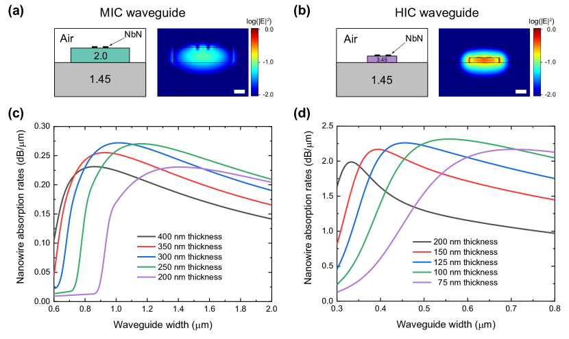
In this subsection, we first compare the absorption rates of NbN nanowires integrated with waveguides of different index contrast. As shown in the schematic drawings of Fig. 2(a) and (b), we set the index of the core material as 3.45 and 2.0 for high- and medium-index-contrast (HIC and MIC) waveguides, respectively. The waveguides have the bottom cladding of 1.45 index and air upper cladding. The MIC waveguide could approximately represent a wide range of waveguide platforms, such as SiN23, 26, GaN43, AlN44, 39, diamond27 and LiNbO345, 46 on insulators (SiO2), while GaAs47 and Si22 on insulators could be good examples of HIC waveguide. The U-shaped NbN nanowire is placed atop these waveguides both as absorber and detector via evanescent coupling to the optical mode confined in the waveguides. The complex refractive index of NbN we use in the simulation is measured by ellipsometry48. The thickness, width and gap of the nanowire are set to 5 nm, 80 nm and 120 nm, respectively, based on previous experimental results 8, 7, 49, which could guarantee saturated internal efficiency at 1550 nm wavelength.
By numerically solving the fundamental eigenmode of the waveguide, we extract the effective index of the propagating mode, the imaginary part of which corresponds to the absorption. The nanowire absorption rates can be obtained using the expression in units of , where is the imaginary part of the effective index. We only consider fundamental TE modes in this subsection, since TE modes are more widely used in the PhC cavity design due to their larger photonic bandgap than TM modes.
Figure 2(c) and (d) plot the simulated results of the nanowire absorption rates as a function of the waveguide width for varying MIC and HIC waveguide thickness. For both waveguide designs, the absorption rates show smooth dependence on the waveguide width, and the maximum peaks shift towards smaller width for increased waveguide thickness. For wider and thicker waveguides, the absorption rates decrease due to better confined optical mode and thus weaker evanescent coupling to the nanowire. On the other hand, the absorption rates also drop for narrower and thinner waveguides because of increased mode size and cut-off condition. As a result, the maximum absorption rate of 0.27 dB/m is achieved with a 300 nm-thick and 1m-wide MIC waveguide. For HIC waveguides, we observe almost one order of magnitude enhanced value of 2.3 dB/m occurring around 100 nm thickness and 550 nm width. This huge difference is not surprising, considering more compact mode profile achieved with HIC waveguides in comparison with MIC waveguides, as shown in Fig. 2(a) and (b). The simulation results are also in good agreement with previously reported experimental values22, 23, 24, 26. Therefore, we only focus on the optimization of HIC waveguide design in the following subsections.
III.2 Effect of nanowire geometry
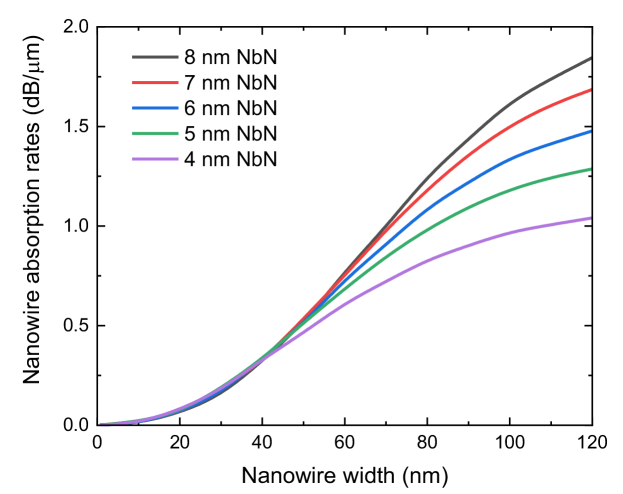
In Fig. 3, we show the effect of the nanowire geometry on its absorption rates. We use the HIC waveguide design shown in Fig. 2(b) in the simulation and set the thickness and width to 220 nm and 600 nm. The gap between the nanowires are kept 1.5 times the width of the nanowire to relieve the current crowding effect50. Interestingly, we observe that the absorption rates are nearly independent of the nanowire thickness in ultra-narrow (<40 nm width) region and start to grow rapidly for larger width beyond this region. We attribute this behavior to the limited penetration of the perpendicularly polarized electric field into the ultra-narrow nanowires, and similar features are also captured and utilized in meander-type SNSPDs before48, 51. The absorption rates tend to saturate with further increased nanowire width (>80 nm) due to displaced nanowire position from the center of the waveguide, where the evanescent field is the strongest. Based on these results, we choose slightly wider 80 nm nanowire of 5 nm-thick in the following discussions, allowing for better electric field penetration into the nanowire, while the nanowire is still narrow and thin enough for obtaining saturated internal efficiencies at the wavelength of 1550 nm7, 8, 52.
III.3 Effect of waveguide parameters
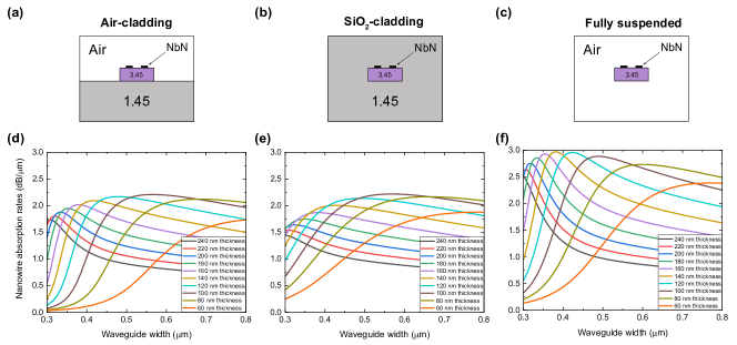
In this subsection, we continue to investigate the absorption rates of the nanowire integrated with waveguides of various types. Following the results of previous sections, we focus on high-index waveguide core material but change the index of upper and bottom claddings, as shown in Fig. 4(a)-(c), which respectively represent the air-cladding waveguide on SiO2, SiO2-cladding buried waveguide and fully suspended waveguide. Here, we only consider fundamental TE modes, since higher-order modes provide substantially reduced absorption rates due to larger mode size. Likewise, we do not show the results of partially etched rib waveguides, which have lower absorption rates compared with ridge waveguides because of larger and pulled-down mode profile24. Figure 4(d)-(f) demonstrate simulated NbN nanowire absorption rates versus waveguide width for varying type and thickness. The highest absorption rates are obtained with fairly thin waveguides of 100-140 nm thickness, which could provide strong evanescent field to couple with the nanowire. In comparison with the other two types of waveguides, the fully suspended waveguide (Fig. 4(f)) shows significantly stronger absorption for a wide range of waveguide width and thickness due to further confined optical mode with higher index contrast.
IV. H0-type PhC cavity integration
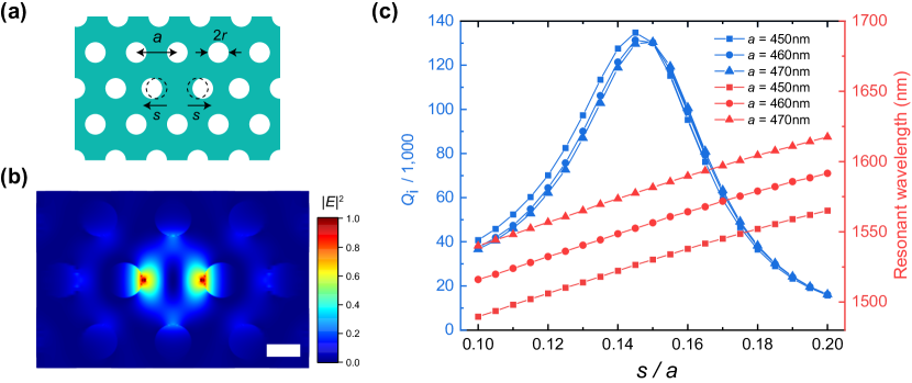
Among a variety of PhC cavities, we choose H0-type cavity (also referred to as “zero-cell” cavity or “point-shift” cavity) due to the ultra-small mode volume and ease of integration with nanowire detectors. As shown in Fig. 5(a) and (b), the cavity is formed by slightly shifting two air holes away from their original positions by in the direction of -K in a two-dimensional hexagonal lattice photonic crystal. Following the previous discussions, we use fully suspended slab made from material of 3.45 index for the PhC cavity design, while the thickness of the slab is chosen to be 220 nm, which is thicker than the optimal value shown in Fig. 4(f), considering the trade-off between large enough band gap of the photonic crystal and strong evanescent field at the top surface where the nanowire is situated.
We first start the optimization of the cavity from a lattice constant of 480 nm to place the center of the band gap at 1550 nm wavelength. Then, iteratively tuning , (shift amount) and (radii of the air holes), the best intrinsic quality factor is obtained with . As shown in Fig. 5(c), the resonant wavelength increases with and , while the highest always occurs around independent of . The decoupled from allows us to adjust the resonance of the cavity to the target wavelength by freely tuning . We choose for the resonant wavelength of 1550 nm, and a of 132k combined with an ultra-small mode volume of is achieved by 3D FDTD simulation.
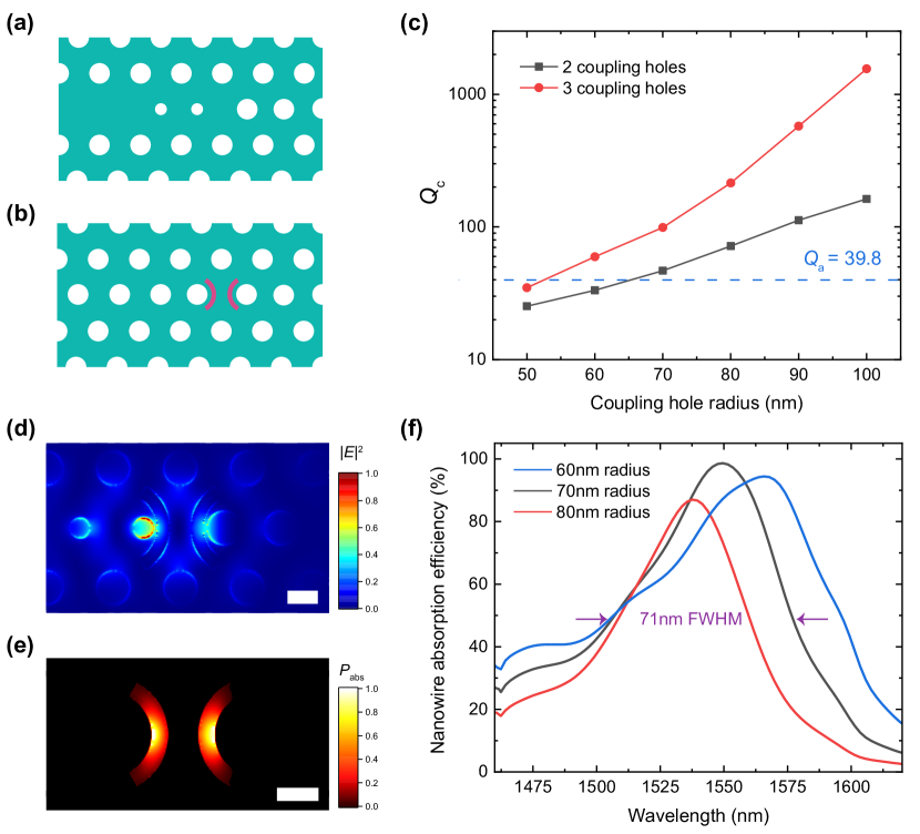
Based on the optimized design of the cavity, we simulate the coupling quality factor () and the absorption quality factor () by either making a partial reflective mirror for the cavity (Fig. 6(a)) or placing a NbN nanowire on the cavity (Fig. 6(b)). In Fig. 6(a), a W1-type PhC waveguide is formed by removing a row of the holes at the left side of the cavity, and a front partial mirror is inserted in between to couple the waveguide to the cavity. The reflectivity of the mirror or the coupling strength could be tuned by changing the number and the radii of the coupling holes making up the mirror. As shown in Fig. 6(b), the NbN nanowire detector comprises two of 120 degree arcs placed atop the slab and adjacent to the inner edges of the two shifted holes forming the cavity. The thickness, width, radius and total length of the nanowire arcs are 5 nm, 80 nm, 265 nm and 1.1 m, respectively. The closest gap between the nanowire and the hole is set to 30 nm, considering a typical alignment tolerance in electron-beam exposure process. Figure 6(c) shows the simulated along with depending on the number and radii of the coupling holes. With the nanowire loaded as a strong absorber, the cavity shows substantially reduced quality factor () in sharp contrast to its . We could obtain near-unity absorption for the nanowire by engineering and fulfilling the critical coupling condition (, equivalent to in Fig. 1(a)). As can be seen in Fig. 6(c), the matching condition requires two coupling holes and the optimal hole radius to be approximately 65 nm.
In order to further investigate the maximum absorption and the frequency response of the nanowire-cavity system, we excite a propagating mode in the coupling PhC waveguide and simulate the absorption by the nanowire as a function of the wavelength around 1550 nm. As shown in Fig. 6(d) and (e), the electric field is strongly confined at the inner edges of the shifted holes, resulting in greatly enhanced power absorption at the center of the nanowire arcs. We note that the electric field and thus the absorption at the ends of the nanowire arcs are very weak, and therefore the nanowires could be quickly tapered to much thicker wires for the electrical connection without introducing much extra absorption in the photon-insensitive area. Figure 6(f) shows the wavelength-dependent nanowire absorption efficiency normalized to the incident power carried by the coupling waveguide. As the size of coupling holes increases, we could clearly see the transition from over-coupling () to under-coupling (). The critical coupling condition is fulfilled with two 70 nm-radius holes, and the maximum absorption of 98.6% is recorded at 1549.6 nm. We attribute the remaining photon loss to the scattering, which could be further reduced by structure optimization, such as individual tuning of the two coupling hole sizes and positions. From the numerically simulated spectrum, the FWHM or 3 dB bandwidth at the critical coupling condition is 71 nm, corresponding to a overall loaded quality factor , which is in good agreement to the prediction results by the method of quality factor matching (Fig. 6(c)), where .
V. Discussion and conclusion
| Reference | Device type | Nanowire length (m) | 3 dB bandwidth (nm) |
Figure of
merit () |
|---|---|---|---|---|
| Ref.37 |
Meander nanowire +
vertical cavity + metal mirror |
1150 | 700 | 0.6 |
| Ref.7 |
Meander nanowire +
vertical cavity + DBR mirror |
1350 | 400 | 0.3 |
| Ref.53 |
Microfiber-coupled
meander nanowire |
1100 | 870 | 0.8 |
| Ref. 35 | Racetrack resonator integration | 1 | 1 | 1 |
| Ref. 34 | 1D-PhC cavity integration | 8.5 | 5.6 | 0.7 |
| Ref. 32 | 1D-PhC cavity integration | 1 | 10 | 10 |
| Ref. 12 | 2D-PhC cavity integration | 3 | 13.2 | 4.4 |
| This work | H0-type PhC cavity integration | 1.1 | 71 | 64.5 |
There is a general trade-off in all cavity-integrated perfect absorber design between the absorption volume and the absorption bandwidth, as derived from Eq. 6. For example, for less absorption volumes (smaller ) or shorter nanowires in the case of cavity-integrated SNSPDs, the photons are expected to experience more round-trips inside the cavity to achieve a near-unity absorption, which entails higher finesse of the cavity (larger for the fixed cavity mode volume) at the expense of reduced bandwidth. Therefore, we introduce a figure of merit defined as bandwidth-nanowire-length ratio to balance the design compromise between and , where is the length of the nanowire required for achieving near-unity maximum absorption, and stands for the 3 dB bandwidth of the nanowire absorption spectrum. Table 1 shows the comparison of our work in terms of , and with other types of recently demonstrated SNSPDs, including meander-type detectors integrated with vertical cavities, detectors integrated with waveguides and various types of on-chip cavities. In comparison with traditional meander-type SNSPDs, our H0-type 2D-PhC cavity design shows two orders of magnitude improved with a dramatically reduced nanowire length down to 1.1 m. In the meanwhile, this design still maintains a significantly enhanced 3 dB bandwidth of 71 nm, compared to other cavity-integrated SNSPDs.
It should also be mentioned that the fully suspended HIC waveguide that our designs are based on could be realized either on Si or GaAs platforms, which benefit the realization of photonic circuits in very compact size. In particular, GaAs has drawn great interest of research recently due to its strong and nonlinearity47, large electro-optic effect54 as well as the capability of on-chip single-photon detector integration25 and quantum dots growth as on-demand single-photon sources55. These excellent optical functionalities renders GaAs a very promising candidate platform for realizing fully integrated quantum photonic circuits with the generation, routing, active manipulation and the final detection of single-photons on a single chip56, 55.
Combined, we expect that our proposed design will enable a large array of high-performance on-chip single-photon detectors for the future fully integrated quantum photonic circuits, simultaneously offering high efficiency, large bandwidth, ultra-low jitter, ultra-fast gigahertz counting rates as well as high fabrication yield.
Acknowledgments
We thank Dr. Xiang Guo and Dr. Linran Fan for the fruitful discussions. We acknowledge funding support from DARPA DETECT program through an ARO grant (No: W911NF-16-2-0151), NSF EFRI grant (EFMA-1640959), AFOSR MURI grant (FA95550-15-1-0029), and the Packard Foundation.
References
- Gol’Tsman et al. 2001 G. Gol’Tsman, O. Okunev, G. Chulkova, A. Lipatov, A. Semenov, K. Smirnov, B. Voronov, A. Dzardanov, C. Williams, and R. Sobolewski, “Picosecond superconducting single-photon optical detector,” Applied Physics Letters 79, 705 (2001).
- Hadfield 2009 R. H. Hadfield, “Single-photon detectors for optical quantum information applications,” Nature Photonics 3, 696 (2009).
- Takesue et al. 2007 H. Takesue, S. W. Nam, Q. Zhang, R. H. Hadfield, T. Honjo, K. Tamaki, and Y. Yamamoto, “Quantum key distribution over a 40-dB channel loss using superconducting single-photon detectors,” Nature Photonics 1, 343 (2007).
- Wang et al. 2018a J. Wang, S. Paesani, Y. Ding, R. Santagati, P. Skrzypczyk, A. Salavrakos, J. Tura, R. Augusiak, L. Mančinska, D. Bacco, et al., “Multidimensional quantum entanglement with large-scale integrated optics,” Science 360, 285 (2018a).
- Liao et al. 2017 S.-K. Liao, W.-Q. Cai, W.-Y. Liu, L. Zhang, Y. Li, J.-G. Ren, J. Yin, Q. Shen, Y. Cao, Z.-P. Li, et al., “Satellite-to-ground quantum key distribution,” Nature 549, 43 (2017).
- Marsili et al. 2013 F. Marsili, V. B. Verma, J. A. Stern, S. Harrington, A. E. Lita, T. Gerrits, I. Vayshenker, B. Baek, M. D. Shaw, R. P. Mirin, et al., “Detecting single infrared photons with 93% system efficiency,” Nature Photonics 7, 210 (2013).
- Zhang et al. 2017 W. Zhang, L. You, H. Li, J. Huang, C. Lv, L. Zhang, X. Liu, J. Wu, Z. Wang, and X. Xie, “NbN superconducting nanowire single photon detector with efficiency over 90% at 1550 nm wavelength operational at compact cryocooler temperature,” Science China Physics, Mechanics & Astronomy 60, 120314 (2017).
- Esmaeil Zadeh et al. 2017 I. Esmaeil Zadeh, J. W. Los, R. B. Gourgues, V. Steinmetz, G. Bulgarini, S. M. Dobrovolskiy, V. Zwiller, and S. N. Dorenbos, “Single-photon detectors combining high efficiency, high detection rates, and ultra-high timing resolution,” APL Photonics 2, 111301 (2017).
- Verma et al. 2019 V. Verma, A. Lita, B. Korzh, E. Wollman, M. Shaw, R. Mirin, and S. Nam, “Towards single-photon spectroscopy in the mid-infrared using superconducting nanowire single-photon detectors,” in Advanced Photon Counting Techniques XIII, Vol. 10978 (International Society for Optics and Photonics, 2019) p. 109780N.
- Marsili et al. 2012 F. Marsili, F. Bellei, F. Najafi, A. E. Dane, E. A. Dauler, R. J. Molnar, and K. K. Berggren, “Efficient single photon detection from 500 nm to 5 m wavelength,” Nano Letters 12, 4799 (2012).
- Cheng et al. 2019a R. Cheng, C.-L. Zou, X. Guo, S. Wang, X. Han, and H. X. Tang, “Broadband on-chip single-photon spectrometer,” Nature Communications 10, 1 (2019a).
- Münzberg et al. 2018 J. Münzberg, A. Vetter, F. Beutel, W. Hartmann, S. Ferrari, W. H. Pernice, and C. Rockstuhl, “Superconducting nanowire single-photon detector implemented in a 2d photonic crystal cavity,” Optica 5, 658 (2018).
- Zhang et al. 2019 W. Zhang, J. Huang, C. Zhang, L. You, C. Lv, L. Zhang, H. Li, Z. Wang, and X. Xie, “A 16-pixel interleaved superconducting nanowire single-photon detector array with a maximum count rate exceeding 1.5 GHz,” IEEE Transactions on Applied Superconductivity 29, 1 (2019).
- Korzh et al. 2018 B. Korzh, Q. Zhao, S. Frasca, J. Allmaras, T. Autry, E. Bersin, M. Colangelo, G. Crouch, A. Dane, T. Gerrits, et al., “Demonstrating sub-3 ps temporal resolution in a superconducting nanowire single-photon detector,” arXiv preprint arXiv:1804.06839 (2018).
- Zadeh et al. 2018 I. E. Zadeh, J. W. Los, R. Gourgues, G. Bulgarini, S. M. Dobrovolskiy, V. Zwiller, and S. N. Dorenbos, “A single-photon detector with high efficiency and sub-10ps time resolution,” arXiv preprint arXiv:1801.06574 (2018).
- Caloz et al. 2019 M. Caloz, B. Korzh, E. Ramirez, C. Schönenberger, R. J. Warburton, H. Zbinden, M. D. Shaw, and F. Bussières, “Intrinsically-limited timing jitter in molybdenum silicide superconducting nanowire single-photon detectors,” arXiv preprint arXiv:1906.02073 (2019).
- Schuck et al. 2013a C. Schuck, W. H. Pernice, and H. X. Tang, “Waveguide integrated low noise NbTiN nanowire single-photon detectors with milli-Hz dark count rate,” Scientific Reports 3, 1893 (2013a).
- Shibata et al. 2015 H. Shibata, K. Shimizu, H. Takesue, and Y. Tokura, “Ultimate low system dark-count rate for superconducting nanowire single-photon detector,” Optics Letters 40, 3428 (2015).
- Cheng et al. 2017 R. Cheng, M. Poot, X. Guo, L. Fan, and H. X. Tang, “Large-area superconducting nanowire single-photon detector with double-stage avalanche structure,” IEEE Transactions on Applied Superconductivity 27, 1 (2017).
- Kerman et al. 2006 A. J. Kerman, E. A. Dauler, W. E. Keicher, J. K. Yang, K. K. Berggren, G. Gol’Tsman, and B. Voronov, “Kinetic-inductance-limited reset time of superconducting nanowire photon counters,” Applied Physics Letters 88, 111116 (2006).
- Sprengers et al. 2011 J. Sprengers, A. Gaggero, D. Sahin, S. Jahanmirinejad, G. Frucci, F. Mattioli, R. Leoni, J. Beetz, M. Lermer, M. Kamp, et al., “Waveguide superconducting single-photon detectors for integrated quantum photonic circuits,” Applied Physics Letters 99, 181110 (2011).
- Pernice et al. 2012 W. H. Pernice, C. Schuck, O. Minaeva, M. Li, G. Goltsman, A. Sergienko, and H. Tang, “High-speed and high-efficiency travelling wave single-photon detectors embedded in nanophotonic circuits,” Nature Communications 3, 1325 (2012).
- Schuck et al. 2013b C. Schuck, W. H. P. Pernice, and H. X. Tang, “NbTiN superconducting nanowire detectors for visible and telecom wavelengths single photon counting on Si3N4 photonic circuits,” Applied Physics Letters 102, 051101 (2013b).
- Kovalyuk et al. 2013 V. Kovalyuk, W. Hartmann, O. Kahl, N. Kaurova, A. Korneev, G. Goltsman, and W. Pernice, “Absorption engineering of nbn nanowires deposited on silicon nitride nanophotonic circuits,” Optics express 21, 22683 (2013).
- Sahin et al. 2015 D. Sahin, A. Gaggero, J.-W. Weber, I. Agafonov, M. A. Verheijen, F. Mattioli, J. Beetz, M. Kamp, S. Höfling, M. C. van de Sanden, et al., “Waveguide nanowire superconducting single-photon detectors fabricated on GaAs and the study of their optical properties,” IEEE Journal of Selected Topics in Quantum Electronics 21, 1 (2015).
- Kahl et al. 2015 O. Kahl, S. Ferrari, V. Kovalyuk, G. N. Goltsman, A. Korneev, and W. H. Pernice, “Waveguide integrated superconducting single-photon detectors with high internal quantum efficiency at telecom wavelengths,” Scientific reports 5, 10941 (2015).
- Rath et al. 2015 P. Rath, O. Kahl, S. Ferrari, F. Sproll, G. Lewes-Malandrakis, D. Brink, K. Ilin, M. Siegel, C. Nebel, and W. Pernice, “Superconducting single-photon detectors integrated with diamond nanophotonic circuits,” Light: Science & Applications 4, e338 (2015).
- Najafi et al. 2015 F. Najafi, J. Mower, N. C. Harris, F. Bellei, A. Dane, C. Lee, X. Hu, P. Kharel, F. Marsili, S. Assefa, et al., “On-chip detection of non-classical light by scalable integration of single-photon detectors,” Nature Communications 6, 5873 (2015).
- Li et al. 2016 J. Li, R. A. Kirkwood, L. J. Baker, D. Bosworth, K. Erotokritou, A. Banerjee, R. M. Heath, C. M. Natarajan, Z. H. Barber, M. Sorel, et al., “Nano-optical single-photon response mapping of waveguide integrated molybdenum silicide (MoSi) superconducting nanowires,” Optics Express 24, 13931 (2016).
- Ferrari et al. 2018 S. Ferrari, C. Schuck, and W. Pernice, “Waveguide-integrated superconducting nanowire single-photon detectors,” Nanophotonics 7 (2018).
- Gaggero et al. 2019 A. Gaggero, F. Martini, F. Mattioli, F. Chiarello, R. Cernansky, A. Politi, and R. Leoni, “Amplitude-multiplexed readout of single photon detectors based on superconducting nanowires,” Optica 6, 823 (2019).
- Vetter et al. 2016 A. Vetter, S. Ferrari, P. Rath, R. Alaee, O. Kahl, V. Kovalyuk, S. Diewald, G. N. Goltsman, A. Korneev, C. Rockstuhl, et al., “Cavity-enhanced and ultrafast superconducting single-photon detectors,” Nano Letters 16, 7085 (2016).
- Calandri et al. 2016 N. Calandri, Q.-Y. Zhao, D. Zhu, A. Dane, and K. K. Berggren, “Superconducting nanowire detector jitter limited by detector geometry,” Applied Physics Letters 109, 152601 (2016).
- Akhlaghi et al. 2015 M. K. Akhlaghi, E. Schelew, and J. F. Young, “Waveguide integrated superconducting single-photon detectors implemented as near-perfect absorbers of coherent radiation,” Nature Communications 6, 8233 (2015).
- Tyler et al. 2016 N. A. Tyler, J. Barreto, G. E. Villarreal-Garcia, D. Bonneau, D. Sahin, J. L. O’Brien, and M. G. Thompson, “Modelling superconducting nanowire single photon detectors in a waveguide cavity,” Optics Express 24, 8797 (2016).
- Yariv 2002 A. Yariv, “Critical coupling and its control in optical waveguide-ring resonator systems,” IEEE Photonics Technology Letters 14, 483 (2002).
- Wang et al. 2016 Y. Wang, H. Li, L. You, C. Lv, J. Huang, W. Zhang, L. Zhang, X. Liu, Z. Wang, and X. Xie, “Broadband near-infrared superconducting nanowire single-photon detector with efficiency over 50%,” IEEE Transactions on Applied Superconductivity 27, 1 (2016).
- Bogaerts et al. 2011 W. Bogaerts, P. D. Heyn, T. V. Vaerenbergh, K. D. Vos, S. K. Selvaraja, T. Claes, P. Dumon, P. Bienstman, D. V. Thourhout, and R. Baets, “Silicon microring resonators,” Laser & Photonics Reviews 6, 47 (2011).
- Guo et al. 2017 X. Guo, C.-l. Zou, C. Schuck, H. Jung, R. Cheng, and H. X. Tang, “Parametric down-conversion photon-pair source on a nanophotonic chip,” Light: Science & Applications 6, e16249 (2017).
- Fan et al. 2018 L. Fan, C.-L. Zou, R. Cheng, X. Guo, X. Han, Z. Gong, S. Wang, and H. X. Tang, “Superconducting cavity electro-optics: A platform for coherent photon conversion between superconducting and photonic circuits,” Science Advances 4, eaar4994 (2018).
- Yablonovitch 1987 E. Yablonovitch, “Inhibited spontaneous emission in solid-state physics and electronics,” Physical Review Letters 58, 2059 (1987).
- Akahane et al. 2003 Y. Akahane, T. Asano, B.-S. Song, and S. Noda, “High-q photonic nanocavity in a two-dimensional photonic crystal,” Nature 425, 944 (2003).
- Xiong et al. 2011 C. Xiong, W. Pernice, K. K. Ryu, C. Schuck, K. Y. Fong, T. Palacios, and H. X. Tang, “Integrated GaN photonic circuits on silicon (100) for second harmonic generation,” Optics Express 19, 10462 (2011).
- Xiong et al. 2012 C. Xiong, W. H. Pernice, X. Sun, C. Schuck, K. Y. Fong, and H. X. Tang, “Aluminum nitride as a new material for chip-scale optomechanics and nonlinear optics,” New Journal of Physics 14, 095014 (2012).
- Wang et al. 2018b C. Wang, M. Zhang, X. Chen, M. Bertrand, A. Shams-Ansari, S. Chandrasekhar, P. Winzer, and M. Lončar, “Integrated lithium niobate electro-optic modulators operating at CMOS-compatible voltages,” Nature 562, 101 (2018b).
- Sayem et al. 2019 A. A. Sayem, R. Cheng, S. Wang, and H. X. Tang, “Lithium-niobate-on-insulator waveguide-integrated superconducting nanowire single-photon detectors,” arXiv preprint arXiv:1912.09418 (2019).
- Chang et al. 2018 L. Chang, A. Boes, X. Guo, D. T. Spencer, M. Kennedy, J. D. Peters, N. Volet, J. Chiles, A. Kowligy, N. Nader, et al., “Heterogeneously integrated GaAs waveguides on insulator for efficient frequency conversion,” Laser & Photonics Reviews 12, 1800149 (2018).
- Anant et al. 2008 V. Anant, A. J. Kerman, E. A. Dauler, J. K. Yang, K. M. Rosfjord, and K. K. Berggren, “Optical properties of superconducting nanowire single-photon detectors,” Optics Express 16, 10750 (2008).
- Cheng et al. 2019b R. Cheng, S. Wang, and H. X. Tang, “Superconducting nanowire single-photon detectors fabricated from atomic-layer-deposited NbN,” Applied Physics Letters 115, 241101 (2019b).
- Clem and Berggren 2011 J. R. Clem and K. K. Berggren, “Geometry-dependent critical currents in superconducting nanocircuits,” Physical Review B 84, 174510 (2011).
- Guo et al. 2015 Q. Guo, H. Li, L. You, W. Zhang, L. Zhang, Z. Wang, X. Xie, and M. Qi, “Single photon detector with high polarization sensitivity,” Scientific reports 5, 9616 (2015).
- Miki et al. 2017 S. Miki, M. Yabuno, T. Yamashita, and H. Terai, “Stable, high-performance operation of a fiber-coupled superconducting nanowire avalanche photon detector,” Optics express 25, 6796 (2017).
- Hou et al. 2019 X. Hou, N. Yao, L. You, H. Li, Y. Wang, W. Zhang, H. Wang, X. Liu, W. Fang, L. Tong, Z. Wang, and X. Xie, “Ultra-broadband microfiber-coupled superconducting single-photon detector,” Optics Express 27, 25241 (2019).
- Wang et al. 2014 J. Wang, A. Santamato, P. Jiang, D. Bonneau, E. Engin, J. W. Silverstone, M. Lermer, J. Beetz, M. Kamp, S. Höfling, et al., “Gallium arsenide (GaAs) quantum photonic waveguide circuits,” Optics Communications 327, 49 (2014).
- Dietrich et al. 2016 C. P. Dietrich, A. Fiore, M. G. Thompson, M. Kamp, and S. Höfling, “GaAs integrated quantum photonics: Towards compact and multi-functional quantum photonic integrated circuits,” Laser & Photonics Reviews 10, 870 (2016).
- Schwartz et al. 2018 M. Schwartz, E. Schmidt, U. Rengstl, F. Hornung, S. Hepp, S. L. Portalupi, K. llin, M. Jetter, M. Siegel, and P. Michler, “Fully on-chip single-photon Hanbury-Brown and Twiss experiment on a monolithic semiconductor–superconductor platform,” Nano Letters 18, 6892 (2018).