An efficient GFET structure
Abstract
A graphene field effect transistor, where the active area is made of monolayer large-area graphene, is simulated including a full 2D Poisson equation and a drift-diffusion model with mobilities deduced by a direct numerical solution of the semiclassical Boltzmann equations for charge transport by a suitable discontinuous Galerkin approach.
The critical issue in a graphene field effect transistor is the difficulty of fixing the off state which requires an accurate calibration of the gate voltages. In the present paper we propose and simulate a graphene field effect transistor structure which has well-behaved characteristic curves similar to those of conventional (with gap) semiconductor materials. The introduced device has a clear off region and can be the prototype of devices suited for post-silicon nanoscale electron technology. The specific geometry overcomes the problems of triggering the minority charge current and gives a viable way for the design of electron devices based on large area monolayer graphene as substitute of standard semiconductors in the active area. The good field effect transistor behavior of the current versus the gate voltage makes the simulated device very promising and a challenging case for experimentalists.
Keywords graphene, GFET, mobility model, drift-diffusion, discontinuous Galerkin method.
1 Introduction
The Metal Oxide Semiconductor Field Effect Transistor (MOSFET) is the backbone of the modern integrated circuits. In the case the active area is made of traditional materials like, for example, silicon or gallium arsenide, a lot of analysis and simulations have been performed in order to optimize the design. Lately a great attention has been devoted to graphene on account of its peculiar features, and in particular, from the point of view of nano-electronics, for the high electrical conductivity. It is highly tempting to try to replace the traditional semiconductors with graphene in the active area of electron devices like the MOSFETs [1] even if many aspect about the actual performance in real applications remain unclear.
Scaling theory predicts that a FET with a thin barrier and a thin gate-controlled region will be robust against short-channel effects down to very short gate lengths. The possibility of having channels that are just one atomic layer thick is perhaps the most attractive feature of graphene for its use in transistors. Main drawbacks of a large-area single monolayer graphene are the zero gap and, for graphene on substrate, the degradation of the mobility. Therefore accurate simulation are warranted for the set up of a viable graphene field effect transistor.
The standard mathematical model is given by the drift-diffusion-Poisson system. Usually the GFETs are investigated by adopting reduced one dimensional models of the Poisson equation with some averaging procedure [2, 3, 4]. Here a full two-dimensional simulation is presented.
A crucial point is the determination of the mobilities entering the drift-diffusion equations. A rather popular model is that proposed in [5]. Here a different approach is adopted. Thanks to the discontinuous Galerkin (DG) scheme developed in [6, 7, 8, 9], we have performed, for graphene on a substrate, an extensive numerical simulation based on the semiclassical Boltzmann equations, including electron-phonon and electron-impuritiy scatterings along with the scattering with remote phonons of the substrate. Both intra and inter-band scatterings have been taken into account. For other simulation approaches the interested reader is referred to [10, 11]. Quantum effects have been also introduced in [12, 13, 14, 15, 16]. An alternative approach could be resorting to hydrodynamical models (see [19, 20]).
From the numerical solutions of the semiclassical Boltzmann equation a model for the mobility functions has been deduced, similarly to what already done in [17] and in [18] in the case of suspended monolayer graphene.
In the present paper we propose a slight different geometry of GFET which leads to a clear and sizable off region, avoiding the problem of triggering the minority charge carriers and producing characteristic curves which seem very promising for the use of large-area graphene in electron devices.
The plan of the paper is as follows. In Sec. 2 the structure of the proposed device is presented along with the mathematical model. In Sec. 3 the mobilities are sketched and in Sec. 4 the numerical simulations of the proposed GFET are shown.
2 Device structure and mathematical model
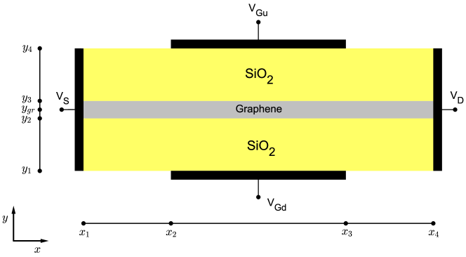
We propose the device with the geometry depicted in Fig. 1. The active zone is made of a single layer of graphene which is between two strips of insulator, both of them being SiO2. The source and drain contacts are directly attached to the graphene. The two gate contacts (up and down) are attached to the oxide. The choice of the type of oxide is not crucial at this stage. We have considered SiO2 as an example. Instead it is crucial to put the source and drain contacts along all the lateral edges for a better control of the electrostatic potential as will be clear from the simulations. In the direction orthogonal to the section the device is considered as infinitely long.
We solve a 2D Poisson equation for the electrostatic potential, assuming that the charge is concentrated on the volume occupied by the atoms composing the graphene layer. Accordingly, the surface charge density of graphene is supposed to be spanned on its thickness which experimental measurements refer between 0.4 nm and 1.7 nm [21]. In order to simulate the current flowing in the channel we adopt the 1D bipolar drift-diffusion model, coupled to the Poisson equation for the electrostatic potential in the whole section. A special attention is required by the initial carrier density profiles that have to be determined compatibly with the electric potential, leading to a nonlinear Poisson equation as discussed in the following.
The bipolar drift-diffusion model is adopted in and it reads
where , are the electron and hole densities in graphene respectively, at time and position , is the thermal voltage, being the positive elementary charge, is the Boltzmann constant, is the lattice temperature (kept constant). The functions and are the mobilities for electrons and holes respectively and is the electric potential, here evaluated on , being the average -coordinate of the graphene sheet (see Fig. 1). The generation and recombination terms are set equal to zero [18]. Indeed, this relation is strictly valid at steady state but here will be assumed during the transient as well. We expect that the stationary solutions is not affected by such an approximation. A typical behavior of the total generation and recombination term versus time, obtained with the DG method [6, 7, 8, 9], can be found in [22].
The system is solved in the interval augmented with Dirichlet boundary conditions for electron and hole densities as will be explained below.
The electric potential solves the 2D Poisson equation
| (1) |
where if and otherwise, and is given by if and otherwise. Here and are the dielectric constants of the graphene and oxide (SiO2) respectively, being the dielectric constant in the vacuum; is the width of the graphene layer which is assumed to be 1 nm (values between 0.4 and 1.7 nm are reported in [21]). The charge in the graphene layer is considered as distributed in the volume enclosed by the parallelepiped of base the area of the graphene and height . Recall that and are areal densities. Dirichlet conditions are imposed on the gate contacts and homogeneous Neumann conditions on the external oxide edges. A major issue is to model the source and drain regions where metal and graphene touch. We assume that source and drain are thermal bath reservoirs of charges which obey a Fermi-Dirac distribution. The injection of charges is determined by a work function . Indeed it depends on the specific material the contacts are made of. We set which is appropriate for Cu within the experimentally reported range of 0.20 eV [23] and 0.30 eV [24].
As summary the following boundary conditions for the electric potential are imposed
Here is the bias voltage, is the source potential, is the source potential, is the upper gate potential, is the down gate potential. is the gate bias potential which is considered equal at both the gate contacts. denotes the normal derivative.
In graphene a sort of doping is induced by the electrostatic potential [25] which leads to a shift of the Fermi energy. Assuming thermal equilibrium, the initial carrier densities and of electrons and holes respectively are related to the electric potential by
being the Fermi-Dirac distribution
where is the Fermi level (in pristine graphene ), is the graphene dispersion relation (strictly valid around the Dirac points), which is the same for electrons and holes (see [26, 27, 28]), is the reduced Planck constant and is the Fermi velocity. The crystal momentum of electrons and holes is assumed to vary over . The boundary conditions at the contacts are given by
| (3) |
Altogether, in order to get the initial density profile as function of the electric potential, we must solve the following nonlinear Poisson equation
| (4) |
augmented with the boundary conditions (3), where
| (5) |
3 Mobility model
We adopt the mobilities deduced in [22] from a direct numerical simulation of the transport equations by using a DG scheme (the interested reader is referred to [7, 9] for the details). The behaviour is the same for holes on account of the symmetry between the hole and electron distributions.
The low field mobility has the expression
where the fitting parameters have been estimated by the least squares method as follows = 0.2978 m2/V ps , 4.223 m2/V ps, = 376.9 m-2, 0.2838, = 2.216, = 4.820, = 68.34 and = 2.372.
The complete mobility model is given by (see also [18],[17])
| (6) |
where , , , , and are fitting parameters.
We have calculated the coefficients , , , , and by means of least square method for several value of the electron density , obtaining the data reported in Tab. 1. The values of the density correspond to the Fermi energies 0.1, 0.2, 0.3, 0.4, 0.5 eV.
| 4471.0 | 0.05265 | 1.034 | 2.135 | 1.059 | 14.53 | 12.78 |
| 15500.0 | 0.02126 | 0.4615 | 1.584 | 0.4276 | 21.77 | 33.3 |
| 33877.0 | 0.1096 | 1.344 | 2.52 | 1.457 | 4.595 | 6.579 |
| 59588.0 | 0.1776 | 2.304 | 3.099 | 1.335 | 1.395 | 1.251 |
| 92644.0 | 0.05047 | 1.988 | 2.661 | 1.109 | 0.8816 | 1.915 |
In each interval a third degree polynomial interpolation has been adopted for the parameters , , , , and [22].
4 Numerical simulations
The GFET of Fig. 1 has been intensively simulated. We have set the length 100 nm, the width of the lower and upper oxide (SiO2) 10 nm. The source and drain contacts are long 50 nm. The lateral contacts are long 21 nm. The two gate potentials are set equal in the simulated cases. We considered a mesh of 40 grid points along the -direction and 23 grid points along the y-direction. In the graphene layer a single row of 40 nodes has been employed. In order to get the solution the following strategy has been adopted: first the Poisson equation is solved by keeping the charge in the graphene layer equal to and for electron and holes, respectively; then the nonlinear Poisson problem (4) is solved with an iterative scheme, by taking as initial guess the solution of the previous step; once the initial data for the electron and hole density have been determined, the full transient drift-diffusion-Poisson system is solved until the steady state is reached. One gets the stationary regime in about three picoseconds.
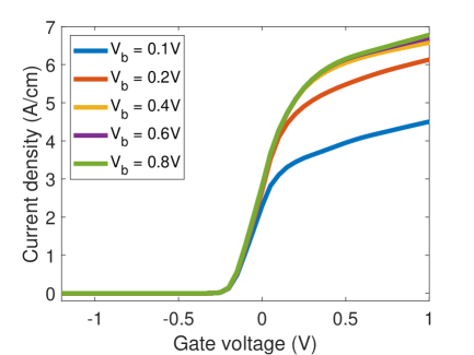
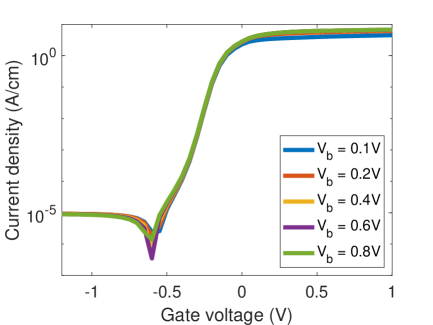
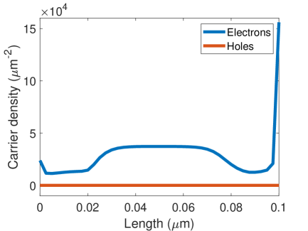
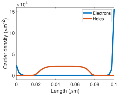
The characteristic curves are shown in Fig.s 2. It is evident that an acceptable field effect transistor is obtained. By decreasing the gate voltage the current settles at a very low value. The plot in logarithmic scale shows a current-on/current-off ratio of five orders of magnitudo at least. The minority charges are only slightly activated and the inversion gate voltage observed with other geometries [1] is practically not present. From Fig.s 3 it is evident that the hole density remains negligible with respects to the majority one. The main reason for such an effect is the peculiar position and breadth of the source and drain contacts which create an electrostatic potential such that the electron total energy is always of constant sign. Devising a working structure has required a full 2D numerical solution of the Poisson equation. The common use of lumped 1D models for the electrostatic potential has the drawback of hiding the effects related to the source and drain contact position and breadth. The simulations have been also performed adopting the mobility model in [5].
The results are qualitatively in good agreement with those obtained by using the mobility model of Sec. 3. Therefore we are rather confident that the efficient FET performance of the proposed device is not an artifact related to the adopted specific mobility model but a general feature stemming from the chosen geometry. The proposed device overcomes the drawback related to the zero gap in pristine large area graphene and represent a viable prototype for for the design of GFETs.
5 Acknowledgements
The authors acknowledge the support from INdAM (GNFM). This work has been supported by the Università degli Studi di Catania, Piano della Ricerca 2016/2018 Linea di intervento 2.
References
- [1] F. Schwierz, “Graphene transistors,” Nat. Nanotechnol., vol. 5, pp. 487-496, July 2010, doi: 10.1038/nnano.2010.89.
- [2] D. Jiménez, and O. Moldovan, “Explicit Drain-Current Model of Graphene Field-Effect Transistors Targeting Analog and Radio-Frequency Applications,” IEEE Trans. Electron Devices, vol. 58, no. 11, pp. 4049-4052, Nov. 2011, doi: 10.1109/TED.2011.2163517.
- [3] A. K. Upadhyay, A. K. Kushwaha, and S. K. Vishvakarma, “A Unified Scalable Quasi-Ballistic Transport Model of GFET for Circuit Simulations,” IEEE Trans. Electron Devices, vol. 65, no. 2, pp. 739-746, Feb. 2018, doi: 10.1109/TED.2017.2782658.
- [4] I. Meric, M. Y. Han, A. F. Young, B. Ozyilmaz, P. Kim, and K. L. Shepard, “Current saturation in zero-bandgap, top-gated graphene field-effect transistors,” Nat. Nanotechnol., vol. 3, pp. 654-659, Nov. 2008, doi: 10.1038/nnano.2008.268.
- [5] V. E. Dorgan, M.-H. Bae, and E. Pop, “Mobility and saturation velocity in graphene on SiO2,” Appl. Phys. Lett., vol. 97, no. 8, Aug. 2020, Art. no. 082112, doi: 10.1063/1.3483130.
- [6] V. Romano, A. Majorana, and M. Coco, “DSMC method consistent with the Pauli exclusion principle and comparison with deterministic solutions for charge transport in graphene,” J. Comp. Physics, vol. 302, pp. 267-284, Dec. 2015, doi: 10.1016/j.jcp.2015.08.047.
- [7] M. Coco, A. Majorana, and V. Romano, “Cross validation of discontinuous Galerkin method and Monte Carlo simulations of charge transport in graphene on substrate,” Ricerche Mat., vol. 66, pp. 201-220, June 2017, doi: 10.1007/s11587-016-0298-4.
- [8] M. Coco, A. Majorana, G. Nastasi, and V. Romano, “High-field mobility in graphene on substrate with a proper inclusion of the Pauli exclusion principle,” Atti Accad. Pelorit. Pericol. Cl. Sci. Fis. Mat. Nat., vol. 96, no. S1, May 2019, Art. no. A6, doi: 10.1478/AAPP.97S1A6.
- [9] A. Majorana, G. Nastasi, and V. Romano, “Simulation of Bipolar Charge Transport in Graphene by Using a Discontinuous Galerkin Method,” Commun. Comput. Phys., vol. 26, no. 1, pp. 114-134, Feb. 2019, doi: 10.4208/cicp.OA-2018-0052.
- [10] P. Lichtenberger, O. Morandi, and F. Schürrer, “High-field transport and optical phonon scattering in graphene,” Phys. Rev. B, vol. 84, no. 4, July 2011, Art. no. 045406, doi: 10.1103/PhysRevB.84.045406.
- [11] O. Muscato, and W. Wagner, “A class of stochastic algorithms for the Wigner equation,” SIAM J. Sci. Comput., vol. 38, no. 3, pp. A1483-A1507, May 2016, doi: 10.1137/16M105798X.
- [12] L. Barletti, “Hydrodynamic equations for electrons in graphene obtained from the maximum entropy principle,” J. Math. Phys., vol. 55, no. 8, July 2014, Art. no. 083303, doi: 10.1063/1.4886698.
- [13] O. Morandi, and F. Schürrer, “Wigner model for quantum transport in graphene,” J. Phys. A: Math. Theor., vol. 44, no. 26, May 2011, Art. no. 265301, doi: 10.1088/1751-8113/44/26/265301.
- [14] L. Luca, and V. Romano, “Quantum corrected hydrodynamic models for charge transport in graphene,” Ann. of Phys., vol. 406, pp. 30-53, July 2019, doi: 10.1016/j.aop.2019.03.018.
- [15] G. Mascali, and V. Romano, “Charge Transport in Graphene including Thermal Effects,” SIAM J. Appl. Math., vol. 77, no. 2, pp. 593-613, Apr. 2017, doi: 10.1137/15M1052573.
- [16] G. Mascali, and V. Romano, “Exploitation of the Maximum Entropy Principle in Mathematical Modeling of Charge Transport in Semiconductors,” Entropy, vol. 19, no. 1, Jan. 2017, Art. no. 36, doi: 10.3390/e19010036.
- [17] A. Majorana, G. Mascali, and V. Romano, “Charge transport and mobility in monolayer graphene,” J. of Mathematics in Industry, vol. 7, Aug. 2016, Art. no. 4, doi: 10.1186/s13362-016-0027-3.
- [18] G. Nastasi, and V. Romano, “Improved mobility models for charge transport in graphene,” Commun. Appl. Ind. Math., vol. 10, pp. 41-52, May 2019, doi: 10.1515/caim-2019-0011.
- [19] V. D. Camiola, and V. Romano, “Hydrodynamical Model for Charge Transport in Graphene,” J. Stat. Phys., vol. 157, no. 6, pp. 1114-1137, Dec. 2014, doi: 10.1007/s10955-014-1102-z.
- [20] L. Luca, and V. Romano, “Comparing linear and nonlinear hydrodynamical models for charge transport in graphene based on the Maximum Entropy Principle,” Int. J. Non-Linear Mech., vol. 104, pp. 39-58, Sept. 2018, doi: 10.1016/j.ijnonlinmec.2018.01.010.
- [21] C. J. Shearer, A. D. Slattery, A. J. Stapleton, J. G. Shapter, and C. T. Gibson, “Accurate thickness measurement of graphene,” Nanotechnology, vol. 27, no. 12, Feb. 2016, Art. no. 125704, doi: 10.1088/0957-4484/27/12/125704.
- [22] G. Nastasi, and V. Romano, “A full coupled drift-diffusion-Poisson simulation of a GFET,” preprint 2019.
- [23] O. Frank, J. Vejpravova, V. Holy, L. Kavan, and M. Kalbac, “Interaction between graphene and copper substrate: The role of lattice orientation,” Carbon, vol. 68, pp. 440-451, Mar. 2014, doi: 10.1016/j.carbon.2013.11.020.
- [24] A. L. Walter, S. Nie, A. Bostwick, K. S. Kim, L. Moreschini, Y. J. Chang, D. Innocenti, K. Horn, K. F. McCarty and E. Rotenberg, “Electronic structure of graphene on single-crystal copper substrates,” Phys. Rev. B, vol. 84, no. 19, Nov. 2011, Art. no. 195443, doi: 10.1103/PhysRevB.84.195443.
- [25] G. M. Landauer, D. Jiménez, J. L. Gonzàlez, “An Accurate and Verilog-A Compatible Compact Model for Graphene Field-Effect Transistors,” IEEE Trans. Nanotechnol., vol. 13, no. 5, pp. 895-904, Sept. 2014, doi: 10.1109/TNANO.2014.2328782.
- [26] C. Jacoboni, “Semiconductors,” in Theory of Electron Transport in Semiconductors, 1st ed. Berlin Heidelberg, Germany: Springer-Verlag, 2010, pp. 103-123.
- [27] C. Kittel, “Semiconductor Crystals,” in Introduction to Solid State Physics, 7th ed. Hoboken, NJ, USA: John Wiley & Sons, Inc., 2005, pp. 185-219.
- [28] A. H. Castro Neto, F. Guinea, N. M. R. Peres, K. S. Novoselov and A. K. Geim, “The electronic properties of graphene,” Rev. of Mod. Phys., vol. 81, no. 1, pp. 109-162, Jan. 2009, doi: 10.1103/RevModPhys.81.109.