RapidLayout: Fast Hard Block Placement
of FPGA-optimized Systolic Arrays
using Evolutionary Algorithms
Abstract
Evolutionary algorithms can outperform conventional placement algorithms such as simulated annealing, analytical placement as well as manual placement on metrics such as runtime, wirelength, pipelining cost, and clock frequency when mapping FPGA hard block intensive designs such as systolic arrays on Xilinx UltraScale+ FPGAs. For certain hard-block intensive, systolic array accelerator designs, the commercial-grade Xilinx Vivado CAD tool is unable to provide a legal routing solution without tedious manual placement constraints. Instead, we formulate an automatic FPGA placement algorithm for these hard blocks as a multi-objective optimization problem that targets wirelength squared and maximum bounding box size metrics. We build an end-to-end placement and routing flow called RapidLayout using the Xilinx RapidWright framework. RapidLayout runs 5–6 faster than Vivado with manual constraints and eliminates the weeks-long effort to generate placement constraints manually for the hard blocks. We also perform automated post-placement pipelining of the long wires inside each convolution block to target 650 MHz URAM-limited operation. RapidLayout outperforms (1) the simulated annealer in VPR by 33% in runtime, 1.9–2.4 in wirelength, and 3–4 in bounding box size, while also (2) beating the analytical placer UTPlaceF by 9.3 in runtime, 1.8–2.2 in wirelength, and 2–2.7 in bounding box size. We employ transfer learning from a base FPGA device to speed-up placement optimization for similar FPGA devices in the UltraScale+ family by 11–14 than learning the placements from scratch.
I Introduction
Modern high-end FPGAs provide high compute density with a heterogeneous mixture of millions of classic lookup tables and programmable routing network along with tens of thousands of DSP and RAM hard blocks. These hard blocks offer ASIC-like density and performance for signal processing functions and on-chip SRAM access. For example, Xilinx UltraScale+ VU11P is equipped with 960 UltraRAM blocks, 4032 Block RAM slices, and 9216 DSP48 blocks capable of operating at 650–891 MHz frequencies which are typically unheard of with LUT-only designs. Furthermore, these hard blocks provide specialized nearest-neighbour interconnect for high-bandwidth, low-latency cascade data movement. These features make it particularly attractive for building systolic neural network accelerators such as CLP [29, 28], Cascades [27], and Xilinx SuperTile [35, 34].
Exploiting the full capacity of FPGA resources including hard blocks at high clock frequency is challenging. The CLP designs presented in [29, 28] only operate at 100–170 MHz on Virtex-7 FPGAs but leave DSPs unused. The Xilinx SuperTile [35, 34] designs run at 720 MHz, but leave half of the DSPs unused, and also waste URAM bandwidth by limiting access. The chip-spanning 650 MHz 19209 systolic array design for the VU11P FPGA [27] requires 95% or more of the hard block resources but fails to route in commercial-grade Xilinx Vivado run with high effort due to congestion. Manual placement constraints are necessary to enable successful bitstream generation, but this requires weeks of painful trial-and-error effort and visual cues in the Vivado floorplanner for the correct setup. This effort is needed largely due to irregularity and asymmetry of the columnar DSP and RAM fabric and the complex cascade constraints that must be obeyed for the systolic data movement architecture. Once the constraints are configured, Vivado still needs 5–6 hours of compilation time, making design iteration long and inefficient. Furthermore, to ensure high-frequency operation, it becomes necessary to pipeline long wires in the design. Since timing analysis must be done post-implementation, we end up either suffering the long CAD iteration cycles or overprovisioning unnecessary pipelining registers to avoid the long design times.
Given this state of affairs with the existing tools, we develop RapidLayout: an alternative, automated, fast placement approach for hard block designs. It is important that such a toolflow addresses the shortcomings of the manual approach by (1) discovering correct placements quickly without the manual trial-and-error loop through slow Vivado invocations, (2) encoding the complex placement restrictions of the data movement within the systolic architecture in the automated algorithm, (3) providing fast wirelength estimation to permit rapid objective function evaluation of candidate solutions, and (4) exploiting design symmetry and overcoming irregularity of the columnar FPGA hard block architecture. Given this wish list, we used the Xilinx RapidWright framework for our tool.
At its core, the toolflow is organized around the design of a novel evolutionary algorithm formulation for hard block placement on the FPGA through multi-objective optimization of wirelength squared and bounding box metrics. Given the rapid progress in machine learning tools, there is an opportunity to revisit conventional CAD algorithms [5], including those in this paper, and attack them with this new toolbox.
The key contributions of this work are listed as follows:
-
We formulate a novel FPGA placement problem for tens of thousands of hard blocks as a multi-objective optimization using evolutionary techniques.
-
We quantify QoR metrics including runtime, wirelength, bounding box size, clock frequency, and pipelining cost for the evolutionary placement algorithms NSGA-II and CMA-ES. We compare these metrics against conventional Simulated Annealing (SA), Genetic Algorithm (GA), Versatile-Place-and-Route (VPR) [22], and the state-of-art analytical placer UTPlaceF [19].
-
We build an end-to-end RapidLayout placement-and-routing toolflow using the open-source Xilinx RapidWright framework.
-
We develop the transfer learning process for hard block placement to accelerate placement optimization through migrating existing placement from base devices to similar devices in the UltraScale+ family (VU3P–VU13P).
II Background
We first discuss the hard block intensive systolic array accelerator optimized for the Xilinx UltraScale+ FPGAs. Next, we discuss the Xilinx RapidWright framework for programming FPGAs through a non-RTL design flow. Then, we describe previous research on FPGA placement algorithms. Finally, we review the classic NSGA-II algorithm and the state-of-art CMA-ES algorithm and compare them with previous evolutionary placement efforts.
II-A FPGA-optimized Systolic Array Accelerator
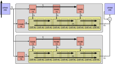
Systolic arrays [14, 16] are tailor-made for convolution and matrix operations needed for neural network acceleration. They are constructed to support extensive data reuse through nearest-neighbor wiring between a simple 2D array of multiply-accumulate blocks. They are particularly amenable to implementation on the Xilinx UltraScale+ architecture with cascade nearest-neighbor connections between DSP, BRAM, and URAM hard blocks. We utilize the systolic convolutional neural network accelerator presented in [27] and illustrated in Figure 1. The key repeating computational block is a convolution engine optimized for the commonly-used 33 convolution operation. This is implemented across a chain of 9 DSP48 blocks by cascading the accumulators. Furthermore, row reuse is supported by cascading three BRAMs to supply data to a set of three DSP48s each. Finally, the URAMs are cascaded to exploit all-to-all reuse between the input and output channels in one neural network layer. Overall, when replicated to span the entire FPGA, this architecture uses 95–100% of the DSP, BRAM, and URAM resources of the high-end UltraScale+ VU37P device. When mapped directly using Vivado without any placement constraints, the router runs out of wiring capacity to fit the connections between these blocks. Since the convolution block is replicated multiple times to generate the complete accelerator, it may appear that placement should be straightforward. However, due to irregular interleaving of the hard block columns, and the non-uniform distribution of resources, the placement required to fit the design is quite tedious and takes weeks of effort.
II-B RapidWright
In this paper, we develop our tool based on the Xilinx RapidWright [17] open-source FPGA framework. It aims to improve FPGA designers’ productivity and design QoR (quality of result) by composing large FPGA designs through a pre-implemented and modular methodology. RapidWright provides high-level Java API access to low-level Xilinx device resources. It supports design generation, placement, routing, and allows design checkpoint (DCP) integration for seamless inter-operability with Xilinx Vivado CAD tool to support custom flows. It also provides access to device geometry information that enables wirelength calculations crucial for tools that aim to optimize timing.
II-C FPGA Placement
FPGA placement maps a clustered logical circuit to an array of fixed physical components to optimize routing area, critical path, power efficiency, and other metrics. FPGA placement algorithms can be broadly classified into four categories: (1) classic min-cut partitioning [31, 23, 24], (2) popular simulated-annealing-based methods [15, 3, 2, 22], (3) analytical placement currently used in FPGA CAD tools [1, 9, 19, 8], and (4) esoteric evolutionary approaches [32, 4, 13]. Min-cut algorithm worked well on small FPGA capacities by iteratively partitioning the circuit to spread the cells across the device. Simulated Annealing was the popular choice for placement until recently. It operates by randomly swapping clusters in an iterative, temperature-controlled fashion resulting in progressively higher quality results. Analytical placers are currently industry standard as they solve the placement problem using a linear algebraic approach that delivers higher quality solutions with less time than annealing. For example, Vivado uses an analytical placement to optimize timing, congestion, and wirelength [8].
II-D Evolutionary Algorithms
There have been several attempts to deploy evolutionary algorithms for FPGA placement with limited success. The earliest one by Venkatraman and Patnaik [32] encodes each two-dimensional block location in a gene and evaluates the population with a fitness function for critical path and area-efficiency. More recently, P. Jamieson [11], [12] points out that GAs for FPGA placement are inferior to annealing mainly due to the crossover operator’s weakness and proposed a clustering technique called supergenes [13] to improve its performance.
In this paper, we design a novel combinational gene representation for FPGA hard block placement and explore two evolutionary algorithms:
-
1.
NSGA-II: Non-Dominated Sorting Genetic Algorithm (NSGA-II [6]) is a two-decade-old multi-objective evolutionary algorithm that has grown in popularity today for Deep Reinforcement Learning [18] and Neural Architecture Search [20] applications. NSGA-II addresses multi-objective selection with non-dominated filtering and crowd distance sorting, which allow the algorithm to effectively explore the solution space and preserve good candidates.
-
2.
CMA-ES: Covariance Matrix Adaptation Evolutionary Strategy (CMA-ES) is a continuous domain optimization algorithm for non-linear, ill-conditioned, black-box problems [10]. CMA-ES models candidate solutions as samplings of an -dimensional Gaussian variable with mean and covariance matrix . At each evolutionary iteration, the population is generated by sampling from with updated mean and covariance matrix. Here, crossover and mutation become adding Gaussian noise to the samplings, which overcomes the weakness of GA’s crossover operator. We use the high-dimensional variant proposed in [26] for fast operation in our placement challenge.


III RapidLayout
The challenge for mapping FPGA-optimized systolic arrays to the Xilinx UltraScale+ device is the placement of hard blocks to their non-uniform, irregular, columnar locations on the fabric while obeying the cascade data movement constraints. We first present our problem formulation and then discuss how to embed it into the evolutionary algorithms.
III-A Problem Formulation
To tackle the placement challenge, we formulate the coarse-grained placement of RAMs and DSP blocks as a constrained multi-objective optimization problem. The placement for the rest of the logic i.e. lookup tables (LUTs) and flip-flops (FFs) is left to Vivado’s placer. The multi-objective optimization goal is formalized as follows.
| (1) |
| (2) |
subject to:
| (3) |
| (4) |
| (5) | ||||
In the equations above:
-
denotes a physical hard block to which a logic block is mapped.
-
denotes a convolution unit that contains 2 URAMs, 18 DSPs, and 8 BRAMs.
-
is the Manhattan distance between two physical hard blocks and .
-
is the weight for wirelength estimation. Here we use the number of connections between hard blocks and .
-
is the bounding box rectangle size (width + height) containing the hard blocks of a convolution unit .
-
and denote the RPM absolute grid co-ordinates of hard block that are needed to compute wirelength and bounding box sizes [36].
Understanding the Objective Function: We approximate routing congestion performance with squared wirelength (Equation 1) and critical path length with the maximum bounding box size (Equation 2). These twin objectives try to reduce pipelining requirements while maximizing clock frequency of operation. While these optimization targets may seem odd, we have observed cases where chasing wirelength2 alone has misled the optimizer into generating wide bounding boxes for a few stray convolution blocks. In contrast, optimizing for maximum bounding box alone was observed to be extremely unstable and causing convergence problems. Hence, we choose these two objective functions to restrict the spread of programmable fabric routing resources and reduce the length of critical path between hard blocks and associated control logic fanout.
Understanding Constraints The optimizer only needs to obey three constraints. The region constraint in Equation 3 restricts the set of legal locations for the hard blocks to a particular repeatable rectangular region of size XMAXYMAX on the FPGA. The exclusivity constraint in Equation 4 forces the optimizer to prevent multiple hard blocks from being assigned to the same physical location. The cascade constraint in Equation 5 is the “uphill” connectivity restriction imposed due to the nature of the Xilinx UltraScale+ DSP, BRAM, and URAM cascades. For DSPs and URAMs, it is sufficient to place connected blocks next to each other. For BRAMs, the adjacent block of the same type resides at one block away from the current location. This is because RAMB180 and RAMB181, which are both RAMB18 blocks, are interleaved in the same column.
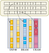
III-A1 Genotype Design for Evolutionary Algorithms
We decompose placement into three sub-problems and encode the candidate solutions with a novel composite genotype design.
-
1.
Distribution Since the systolic array accelerator does not match the hard block resource capacity perfectly, we allocate hard blocks across resource columns according to the distribution genotype.
-
2.
Location Once we choose the exact number of blocks to place on a given resource column, we assign each block in the column a location according to a value between 0 1.
-
3.
Mapping Finally, we label selected blocks and allocate them to each convolution unit according to the mapping genotype. It is a permutation genotype that optimizes the order of elements without changing their values.
In Figure 2, we visualize the genotype design which consists of the three parts just discussed earlier. During evolution, each part of the genotype is updated and decoded independently, but evaluated together.
III-A2 Generality of the Evolutionary Formulation
The problem formulation and genotype design are motivated by a convolutional systolic array. However, the placement formulation is not limited to any particular hard block design. For example, the computing unit (Equation 2) can be any hard block design, as long as the number of hard blocks, their connections, and cascade information are provided.
III-A3 Comparison with Prior Evolutionary Placements
Our genotype design differs from prior works in three aspects: (1) We provide placement support for heterogeneous hard block types. (2) We encode cascade constriants into the genotype, which eschews extra legalization steps and reduces search space. (3) The three-tier gentoype design enables placement transfer learning across devices (Section IV-D).
III-B RapidLayout Design Flow
We now describe the end-to-end RapidLayout design flow:
-
Netlist Replication (<1 s) RapidLayout starts with a synthesized netlist of the convolution unit with direct instantiations of the FPGA hard blocks. The unit design is replicated into the entire logical netlist that maps to the whole Super Logic Region (SLR).
-
Evolutionary Hard Block Placement (30 s-5min) RapidLayout uses NSGA-II or CMA-ES to generate hard block placement for the minimum repeating rectangular region. Then the rectangular layout is replicated (copy-paste) to produce the placement solution for the entire SLR.
-
Placement and Site Routing (3 min) The placement information is embedded in the DCP netlist by placing the hard blocks on the physical blocks called “sites”, followed by “site-routing” to connect intra-site pins.
-
Post-Placement Pipelining (10 s) After finalizing placement, we can compute the wirelength for each net in the design and determine the amount of pipelining required for high-frequency operation. This is done post-placement [33, 7, 30] to ensure the correct nets are pipelined and to the right extent. The objective of this step is to aim for the 650 MHz URAM-limited operation as dictated by the architectural constraints of the systolic array [27].
-
SLR Placement and Routing (55 min) Once the hard blocks are placed and pipelined, we call Vivado to complete LUT/FF placement and routing for the SLR.
-
SLR Replication (1-5 min) The routed design on the SLR is copied across the entire device using RapidWright APIs to complete the overall implementation.
For VU11P device, RapidLayout accelerates the end-to-end implementation by 5–6 when measuring CAD runtime alone (one hour vs. Vivado’s 5–6 hours). This does not include the weeks of manual tuning effort that is avoided by automatically discovering the best placement for the design.
III-C Example Walkthrough
To illustrate how the different steps help produce the full-chip layout, we walk you through the intermediate stages of the flow. We will inspect three stages of placement, going from a single block layout to a repeating rectangle layout, and then onto a full-chip layout.
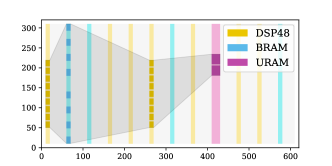
Single Block layout: The floorplan of a single convolution block in isolation is shown in Figure 4, where the hard block columns and chosen resources are highlighted. We also highlight the extent of routing requirements between the hard blocks in gray. The locations of the URAM, BRAM, and DSP columns are irregular, which forces a particular arrangement and selection of resources to minimize wirelength and bounding box size. It is clear that a simple copy-paste of a single block is not workable due to this irregularity.
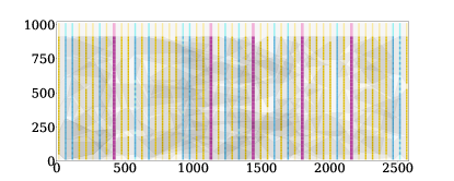
Single Repeating Rectangle Layout: RapidLayout iteratively partitions one SLR and calculates utilizaiton until the divided section does not fit any unit. Then, the partition scheme with the highest utilization rate is selected to determine the repeating rectangular region. In Figure 5, we show the floorplan for such a region. The resource utilization within the rectangle is 100% URAMs, 93.7% DSP48s, and 95.2% BRAMs, which holds for the entire chip after replication. Our optimizer minimizes overlapping and thus reducing routing congestions to permit high-frequency operation.
Full-Chip Layout: The entire chip layout is generated in two steps: (1) First, the rectangular region’s placement is replicated to fill up one SLR (SLR0). The SLR is then pipelined and fully routed. (2) Second, the placement and routing from SLR0’s implementation are replicated across the two other SLRs to fill up the FPGA.
Method NSGA-II CMA-ES SA GA VPR UTPlaceF Manual Runtime (secs) 586 (323) 51 1577 (2.7, 30.8) 850 (1.5, 16.7) 76 (0.13, 1.5) 473 (0.8, 9.3) 1–2 wks Wirelength 3.5K (3.5K) 4.4K 3.1K (0.9, 0.7) 9.2K (2.6, 2.1) 8.5K (2.4, 1.9) 7.8K (2.2, 1.8) 8.1K (2.3, 1.8) BBox 1183 (1543) 1606 1387 (1.2, 0.9) 1908 (1.6, 1.2) 4941 (4.1, 3.1) 3218 (2.7, 2.0) 1785 (1.5, 1.1) Pipeline Reg. 256K (273K) 273K 273K (1.1, 1) 323K (1.3, 1.2) - - 306K (1.2, 1.1) Frequency (MHz) 733 (688) 708 711 (1.03, 0.99) 585 (1.3, 1.2) - - 693 (1.1, 1.02)
IV Results
RapidLayout is implemented in Java to enable seamless integration with RapidWright Java APIs. We use the Java library Opt4J [21] as the optimization framework for NSGA-II, SA, and GA. CMA-ES is implemented with Apache Commons Math Optimization Library [25] 3.4 API. We use VPR 7.0 official release [22] and UTPlaceF TCAD version [19] binary for QoR comparison. All placed designs are routed and timed with Vivado Design Suite 2018.3. We run our experiments on an Ubuntu 16.04 LTS machine with Intel Xeon Gold 5115 CPU (10 cores, 20 threads) and 128 GB DDR4 RAM.
IV-A Performance and QoR Comparison
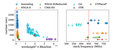
We compare the performance and QoR of evolutionary algorithms against (1) conventional simulated annealing (SA), (2) academic placement tool VPR 7.0, (3) state-of-art analytical placer UTPlaceF, (4) single-objective genetic algorithm (GA) [37], and (5) manual placement design. We exclude RapidWright’s default annealing-based block placer since it does not give feasible placement solutions. We run each placement algorithm 50 times with seeded random initialization. Then, we select the top-10 results for each method to route and report clock frequency. While we include VPR and UTPlaceF in comparison, they do not support cascade constraints (Equation 5). This limits our comparison to an approximate check on solution quality and runtime, and we are unable to translate the resulting placement to the FPGA directly.
In Figure 7a, we plot total runtime and final optimized wirelength2 maximum bounding box size for the different placement algorithms along with Vivado-reported frequency results. We see some clear trends: (1) NSGA-II is 2.7 faster than SA and delivers 1.2 bounding box improvement, but has 12.9% longer wirelength. The average clock frequency of top-10 results is evidently higher than SA as NSGA-II’s performance is more stable. (2) CMA-ES is 30 faster than SA. Although the average bounding box size (16% larger) and wirelength (42% larger) are worse than SA’s results, CMA-ES achieves a slightly higher average clock frequency at 711 MHz. (4) An alternate NSGA-II method discussed later in Section IV-B2 with a reduced search space delivers roughly 5 times shorter runtime than SA, with only 2.8% clock frequency degradation, which is still above the URAM-limited 650 MHz maximum operating frequency.
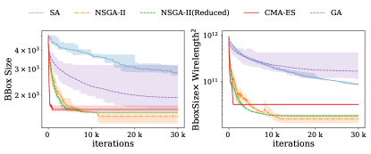
In Figure 7b, we see the convergence rate of the different algorithms when observing bounding box sizes and the combined objective. NSGA-II clearly delivers better QoR after 10 k iterations, while CMA-ES delivers smaller bounding box sizes within a thousand iterations. Across multiple runs, bounding box optimization shows a much more noisy behavior with the exception of CMA-ES. This makes it (1) tricky to rely solely on bounding box minimization, and (2) suggests a preference for CMA-ES for containing critical paths within bounding boxes.
Finally, in Table I, we compare average metric values across the 50 runs of all methods. NSGA-II and CMA-ES deliver superior QoR and runtime against UTPlaceF and VPR, and speeds up runtime by 3–30 against annealing with a minor loss in QoR. Table I also reports the number of registers needed for the 650 MHz operations. NSGA-II delivers this with 17k (6%) less registers against annealing and 50k (16%) less registers against manual placement. NSGA-II results in Table I are run in 20 threads. Although CMA-ES runs in serial, the runtime is 10 faster than NSGA-II with a QoR gap.
IV-B Parameter Tuning for Annealing and NSGA-II
In this section, we discuss cooling schedule selection for annealing and optimizations to NSGA-II to explore quality, runtime tradeoffs.
IV-B1 Parameter Tuning for SA
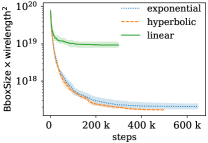
The cooling schedule determines the final placement quality, but it is highly problem-specific. We plot the cooling schedule tuning process in Figure 8 and choose the hyperbolic cooling schedule for placement experiments presented in Table I to achieve the best result quality.
IV-B2 NSGA-II Reduced Genotype
As per the genotype design, distribution and location genotypes take up a large portion of the composite genotype, and they demand quantization and legalization steps. However, for high-utilization designs, distribution and location are less influential since resources are nearly fully utilized. Therefore, we reduce the genotype to mapping only for NSGA-II, and uniformly distribute and stack the hard blocks from bottom to top. As a consequence of this trade-off, we observe a 1.8 runtime improvement but a 1.3 larger bounding box size against original NSGA-II. In the convergence plot of Figure 7b, we discover that reduced genotype does not save iteration needed, and the bulk of the runtime improvements comes from reduced genotype decoding and legalization work.
IV-C Pipelining
Finally, we explore the effect of pipelining stages on different placement algorithms. At each pipelining depth, multiple placements from each algorithm are routed by Vivado to obtain a frequency performance range.
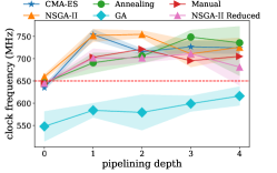
In Figure 9, we show the improvement in frequency as a function of the number of pipeline stages inserted along the long wires by RapidLayout. We note that NSGA-II delivers 650 MHz frequency with no pipelining, while others require at least one stage. Therefore, NSGA-II saves 6%–16% registers at pipelining as shown in Table I. NSGA-II wins over manual design at every depth, and CMA-ES exhibits the most stable performance. Systolic array operation at 750+ MHz should be possible with planned future design refinements. CMA-ES and NSGA-II can deliver 750+ MHz frequency with only two pipeline stages, while SA requires four stages.
IV-D Transfer Learning
Device Design Size Impl.Runtime Frequency (MHz) Placement Runtime (s) (conv units) (mins.) Scratch Transfer Scratch Transfer xcvu3p 123 46.4 718.9 - 428.3 - xcvu5p 246 56.9 677.9 660.5 577.9 42.2 (13.7) xcvu7p 246 55.1 670.2 690.1 578.8 41.9 (13.8) xcvu9p 369 58.4 684.9 662.3 570.8 42.0 (13.6) xcvu11p 480 65.2 655.3 - 522.4 - xcvu13p 640 69.4 653.2 701.3 443.7 38.4 (11.6)
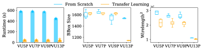
RapidLayout is capable of delivering high-quality placement results on devices with different sizes, resource ratio, or column arrangements with transfer learning ability. Transfer learning uses the genotype of an existing placement as a starting seed for initializing the placement search on a new device. We partition Xilinx UltraScale+ family into two groups with a similar number of hard block columns. We choose VU3P and VU11P as “seed” devices on which RapidLayout generates placement from scratch with NSGA-II. Thereafter, placement results on seed devices are migrated to destination devices in the same group. In Table II and Figure 10, we compare placement runtimes with and without transfer learning across a range of FPGA device sizes. We observe that transfer learning accelerates the optimization process by 11–14 with a frequency variation from -2% to +7%. If we observe the total implementation runtime column, we note that SLR replication ensures that the increase in overall runtime (46 mins.69 mins., 1.5) with device size is much less than the FPGA capacity increase (123640, 5.2).
V Conclusions
We present an end-to-end hard block placement workflow for resource-intensive systolic array designs on modern heterogeneous FPGAs. We show how to outperform conventional simulated annealing and state-of-art analytical placement with evolutionary algorithms on metrics such as runtime, bounding box size, pipelining cost, and clock period. RapidLayout also employs transfer learning to quickly generate placements for similar FPGA devices. RapidLayout is open-source at https://git.uwaterloo.ca/watcag-public/rapidlayout.
VI Acknowledgements
This work was conducted as part of MITACS Globalink Research Internship in 2019. This work has been supported in part by NSERC and CMC Microsystems. This work was also supported by Industry-University Collaborative Education Program between SYSU and Digilent Technology: Edge AI Oriented Open Source Software and Hardware Makerspace, and the State’s Key Project of Research and Development Plan in China under Grants 2017YFE0121300-6. Any opinions, findings, and conclusions or recommendations expressed in this publication are those of the authors and do not necessarily reflect the views of the sponsors.
References
- [1] Z. Abuowaimer, D. Maarouf, T. Martin, J. Foxcroft, G. Gréwal, S. Areibi, and A. Vannelli. Gplace3. 0: Routability-driven analytic placer for ultrascale fpga architectures. ACM Transactions on Design Automation of Electronic Systems (TODAES), 23(5):1–33, 2018.
- [2] V. Betz and J. Rose. Vpr: A new packing, placement and routing tool for fpga research. In International Workshop on Field Programmable Logic and Applications, pages 213–222. Springer, 1997.
- [3] V. Betz, J. Rose, and A. Marquardt. Architecture and cad for deep-submicron fpgas, chapter appendix b, 1999.
- [4] R. Collier, C. Fobel, L. Richards, and G. Grewal. A formal and empirical analysis of recombination for genetic algorithm-based approaches to the fpga placement problem. In 2012 25th IEEE Canadian Conference on Electrical and Computer Engineering (CCECE), pages 1–6. IEEE, 2012.
- [5] J. Dean. The deep learning revolution and its implications for computer architecture and chip design. arXiv preprint arXiv:1911.05289, 2019.
- [6] K. Deb, A. Pratap, S. Agarwal, and T. Meyarivan. A fast and elitist multiobjective genetic algorithm: Nsga-ii. IEEE transactions on evolutionary computation, 6(2):182–197, 2002.
- [7] K. Eguro and S. Hauck. Simultaneous retiming and placement for pipelined netlists. In 2008 16th International Symposium on Field-Programmable Custom Computing Machines, pages 139–148, April 2008.
- [8] T. Feist. Xilinx White Paper: Vivado Design Suite (WP416). Xilinx.
- [9] M. Gort and J. H. Anderson. Analytical placement for heterogeneous fpgas. In 22nd international conference on field programmable logic and applications (FPL), pages 143–150. IEEE, 2012.
- [10] N. Hansen and A. Ostermeier. Adapting arbitrary normal mutation distributions in evolution strategies: The covariance matrix adaptation. In Proceedings of IEEE international conference on evolutionary computation, pages 312–317. IEEE, 1996.
- [11] P. Jamieson. Revisiting genetic algorithms for the fpga placement problem. In GEM, pages 16–22, 2010.
- [12] P. Jamieson. Exploring inevitable convergence for a genetic algorithm persistent fpga placer. In Proceedings of the International Conference on Genetic and Evolutionary Methods (GEM), page 1. The Steering Committee of The World Congress in Computer Science, Computer …, 2011.
- [13] P. Jamieson, F. Gharibian, and L. Shannon. Supergenes in a genetic algorithm for heterogeneous fpga placement. In 2013 IEEE Congress on Evolutionary Computation, pages 253–260. IEEE, 2013.
- [14] N. P. Jouppi, C. Young, N. Patil, D. Patterson, G. Agrawal, R. Bajwa, S. Bates, S. Bhatia, N. Boden, A. Borchers, R. Boyle, P. Cantin, C. Chao, C. Clark, J. Coriell, M. Daley, M. Dau, J. Dean, B. Gelb, T. V. Ghaemmaghami, R. Gottipati, W. Gulland, R. Hagmann, C. R. Ho, D. Hogberg, J. Hu, R. Hundt, D. Hurt, J. Ibarz, A. Jaffey, A. Jaworski, A. Kaplan, H. Khaitan, D. Killebrew, A. Koch, N. Kumar, S. Lacy, J. Laudon, J. Law, D. Le, C. Leary, Z. Liu, K. Lucke, A. Lundin, G. MacKean, A. Maggiore, M. Mahony, K. Miller, R. Nagarajan, R. Narayanaswami, R. Ni, K. Nix, T. Norrie, M. Omernick, N. Penukonda, A. Phelps, J. Ross, M. Ross, A. Salek, E. Samadiani, C. Severn, G. Sizikov, M. Snelham, J. Souter, D. Steinberg, A. Swing, M. Tan, G. Thorson, B. Tian, H. Toma, E. Tuttle, V. Vasudevan, R. Walter, W. Wang, E. Wilcox, and D. H. Yoon. In-datacenter performance analysis of a tensor processing unit. In 2017 ACM/IEEE 44th Annual International Symposium on Computer Architecture (ISCA), pages 1–12, June 2017.
- [15] S. Kirkpatrick, C. D. Gelatt, and M. P. Vecchi. Optimization by simulated annealing. science, 220(4598):671–680, 1983.
- [16] Kung. Why systolic architectures? Computer, 15(1):37–46, Jan 1982.
- [17] C. Lavin and A. Kaviani. Rapidwright: Enabling custom crafted implementations for fpgas. In 2018 IEEE 26th Annual International Symposium on Field-Programmable Custom Computing Machines (FCCM), pages 133–140. IEEE, 2018.
- [18] K. Li, T. Zhang, and R. Wang. Deep reinforcement learning for multi-objective optimization. arXiv preprint arXiv:1906.02386, 2019.
- [19] W. Li, S. Dhar, and D. Z. Pan. Utplacef: A routability-driven fpga placer with physical and congestion aware packing. IEEE Transactions on Computer-Aided Design of Integrated Circuits and Systems, 37(4):869–882, 2017.
- [20] Z. Lu, I. Whalen, V. Boddeti, Y. Dhebar, K. Deb, E. Goodman, and W. Banzhaf. Nsga-net: neural architecture search using multi-objective genetic algorithm. In Proceedings of the Genetic and Evolutionary Computation Conference, pages 419–427. ACM, 2019.
- [21] M. Lukasiewycz, M. Glaß, F. Reimann, and J. Teich. Opt4J - A Modular Framework for Meta-heuristic Optimization. In Proceedings of the Genetic and Evolutionary Computing Conference (GECCO 2011), pages 1723–1730, Dublin, Ireland, 2011.
- [22] J. Luu, J. Goeders, M. Wainberg, A. Somerville, T. Yu, K. Nasartschuk, M. Nasr, S. Wang, T. Liu, N. Ahmed, K. B. Kent, J. Anderson, J. Rose, and V. Betz. Vtr 7.0: Next generation architecture and cad system for fpgas. ACM Trans. Reconfigurable Technol. Syst., 7(2):6:1–6:30, June 2014.
- [23] P. Maidee, C. Ababei, and K. Bazargan. Fast timing-driven partitioning-based placement for island style fpgas. In Proceedings of the 40th annual design automation conference, pages 598–603, 2003.
- [24] P. Maidee, C. Ababei, and K. Bazargan. Timing-driven partitioning-based placement for island style fpgas. IEEE Transactions on Computer-Aided Design of Integrated Circuits and Systems, 24(3):395–406, 2005.
- [25] A. C. Math. Commons math: The apache commons mathematics library, 2013.
- [26] R. Ros and N. Hansen. A simple modification in cma-es achieving linear time and space complexity. In International Conference on Parallel Problem Solving from Nature, pages 296–305. Springer, 2008.
- [27] A. Samajdar, T. Garg, T. Krishna, and N. Kapre. Scaling the cascades: Interconnect-aware fpga implementation of machine learning problems. In 2019 29th International Conference on Field Programmable Logic and Applications (FPL), pages 1–8, Sep. 2019.
- [28] Y. Shen, M. Ferdman, and P. Milder. Overcoming resource underutilization in spatial cnn accelerators. In 2016 26th International Conference on Field Programmable Logic and Applications (FPL), pages 1–4, Aug 2016.
- [29] Y. Shen, M. Ferdman, and P. Milder. Maximizing cnn accelerator efficiency through resource partitioning. In Proceedings of the 44th Annual International Symposium on Computer Architecture, ISCA ’17, pages 535–547, New York, NY, USA, 2017. ACM.
- [30] D. P. Singh and S. D. Brown. Integrated retiming and placement for field programmable gate arrays. In Proceedings of the 2002 ACM/SIGDA Tenth International Symposium on Field-Programmable Gate Arrays, FPGA ’02, page 67–76, New York, NY, USA, 2002. Association for Computing Machinery.
- [31] S. Trimberger and M.-R. Chene. Placement-based partitioning for lookup-table-based fpgas. In Proceedings 1992 IEEE International Conference on Computer Design: VLSI in Computers & Processors, pages 91–94. IEEE, 1992.
- [32] R. Venkatraman and L. M. Patnaik. An evolutionary approach to timing driven fpga placement. In Proceedings of the 10th Great Lakes symposium on VLSI, pages 81–85, 2000.
- [33] N. Weaver, Y. Markovskiy, Y. Patel, and J. Wawrzynek. Post-placement c-slow retiming for the xilinx virtex fpga. In Proceedings of the 2003 ACM/SIGDA Eleventh International Symposium on Field Programmable Gate Arrays, FPGA ’03, page 185–194, New York, NY, USA, 2003. Association for Computing Machinery.
- [34] E. Wu, X. Zhang, D. Berman, and I. Cho. A high-throughput reconfigurable processing array for neural networks. In 2017 27th International Conference on Field Programmable Logic and Applications (FPL), pages 1–4, Sep. 2017.
- [35] E. Wu, X. Zhang, D. Berman, I. Cho, and J. Thendean. Compute-efficient neural-network acceleration. In Proceedings of the 2019 ACM/SIGDA International Symposium on Field-Programmable Gate Arrays, FPGA 2019, Seaside, CA, USA, February 24-26, 2019, pages 191–200, 2019.
- [36] Xilinx. Vivado Design Suite User Guide, Using Constraints (UG903). Xilinx.
- [37] M. Yang, A. Almaini, L. Wang, and P. Wang. An evolutionary approach for symmetrical field programmable gate array placement. In Research in Microelectronics and Electronics, 2005 PhD, volume 1, pages 169–172. IEEE, 2005.