Conductance quantization and shot noise of a double-layer quantum point contact
Abstract
The conductance quantization and shot noise below the first conductance plateau are measured in a quantum point contact fabricated in a GaAs/AlGaAs tunnel-coupled double quantum well. From the conductance measurement, we observe a clear quantized conductance plateau at and a small minimum in the transconductance at . Spectroscopic transconductance measurement reveals three maxima inside the first diamond, thus suggesting three minima in the dispersion relation for electric subbands. Shot noise measurement shows that the Fano factor behavior is consistent with this observation. We propose a model that relates these features to a wavenumber directional split subband due to a strong Rashba spin–orbit interaction that is induced by the center barrier potential gradient of the double-layer sample.
I Introduction
In quantum point contacts (QPCs) on two-dimensional electron gas (2DEG) systems, nanometer-scale confinement embodies a quantum ballistic transport analogous to the transverse modes of optical waveguides. The transverse modes or subbands are well separated in energy; thus, the conductance through a QPC becomes quantized in a unit of van Wees et al. (1988); Wharam et al. (1988); Thomas et al. (1996), where denotes Planck’s constant, the elementary charge, and the coefficient 2 expresses the spin degeneracy that is understood using the Landauer-Büttiker formalism Landauer (1957); Büttiker (1986); Büttiker et al. (1985). Although many theoretical studies suggested the lifted spin degeneracy state ( plateau) at zero magnetic field Bruus et al. (2001); Reilly et al. (2001); Wang and Berggren (1998); Daul and Noack (1998); Yang (2004), this degeneracy is typically not resolved. Instead, a small plateau appears at Thomas et al. (1996), and has attracted considerable interest (for a review, see Micolich (2011)). The Landauer-Büttiker model has been tested by measuring shot noise, i.e., the discrete noise of the charge that is carried by particles in the probabilistic scattering process Büttiker (1990a, 1992); Lesovik (1989); Yurke and Kochanski (1990); Martin and Landauer (1992); Blanter and Büttiker (2000); Kobayashi (2016), in this system. Previous shot noise measurements for QPCs on 2DEGs have contributed significantly to the elucidation of basic physics and complemented the conductance results Kumar et al. (1996); Reznikov et al. (1995); Roche et al. (2004); DiCarlo et al. (2006); Gershon et al. (2008); Hashisaka et al. (2008); Nakamura et al. (2009); Kohda et al. (2012). Furthermore, not only the fundamental physical importance, semiconductor nanostructures with a QPC offer electronic devices that can manipulate electron charges and spins; thus, they are feasible for spintronic devices Wolf et al. (2001); Awschalom and Flatté (2007) and quantum computation Bennett and DiVincenzo (2000). In particular, a QPC on a tunnel-coupled double layer (coupled quantum wire) is a candidate for implementing a qubit Bielejec et al. (2005); Bertoni et al. (2000); Ramamoorthy et al. (2007). Hitherto, several studies Thomas et al. (1999); Salis et al. (1999); Thomas et al. (2000); Nuttinck et al. (2000); Fischer et al. (2006); Smith et al. (2009); Ichinokura et al. (2013) have been conducted that resolved the coupled wavefunction modes of double-layer systems, and the obtained information is useful for quantum engineering. The resolution of spin degeneracy and the generation of spin currents with only electrical controls, such as using spin–orbit interactions (SOIs) Datta and Das (1990); Kohda et al. (2012); Nichele et al. (2015); Quay et al. (2010); Kammhuber et al. (2017); Heedt et al. (2017); Srinivasan et al. (2017); Masuda et al. (2018), remain to be addressed in future studies. In addition, the shot noise for tunnel-coupled QPCs should be measured, because additional degrees of freedom are expected to affect many-body interactions in the nonequilibrium regime Ferrier et al. (2016).
In this study, we fabricated a QPC in a double-layer 2DEG of a GaAs/AlGaAs double quantum well (DQW) sample and investigated the conductance quantization in this double-layer QPC system. Here, we report the shot noise results when the conductance is below the first conductance plateau, . Previously, researchers have reported the coexistence of and plateaus Nuttinck et al. (2000); Crook et al. (2006); Debray et al. (2009); Kohda et al. (2012); Das et al. (2017). Using a high mobility and low electron density double-layer sample, we observed a clear conductance plateau at , and transconductance minima at and at zero magnetic field and the lowest temperature available for the dilution refrigerator used in this experiment. Energy spectroscopy reveals a rich structure of subband edge (SBE) lines with three maxima inside the first SBE diamond, between the and plateaus region. They are dependent on the magnitude and direction of the magnetic fields, and consistent with the horizontal (in wavenumber direction) subband splitting model discussed herein. From the shot noise measurement, the Fano factor , i.e., the current noise normalized to the noise of Poissonian transmission statistics, exhibits reductions at and , and a small reduction at . In addition, we observe a difference in with regard to the positive and negative biases that further suggests an SOI dispersion with Zeeman splitting. We hypothesize that this splitting is caused by the Rashba SOI Bychkov and Rashba (1984) that is induced by a strong potential gradient of the center barrier and the high mobility of the sample. This study would invoke further investigations for spin-related physics and a quasiparticle’s charge in the double-layer system.
The remainder of this paper is structured as follows: In Sec. II, we describe the sample of this experiment (II.1), the experimental setups for conductance measurements (II.2), and the shot noise measurements (II.3). In Sec. III, we present the experimental results on the conductance measurement (III.1) and shot noise measurement (III.2). A discussion is presented in Sec. IV. After calculating the wavefunctions in the DQW at the QPC (IV.1), we discuss the effect of the SOI for the conductance and shot noise (IV.2). We present the conclusions in Sec. V. Future perspectives are presented briefly in this section.
II Experiment
II.1 Sample preparation
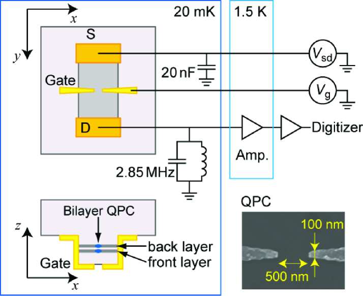
The sample used in this study was fabricated on a DQW heterostructure grown by molecular beam epitaxy on a GaAs (100) surface in the NTT Basic Research Laboratories. The wafer comprises two 20-nm-wide GaAs quantum wells separated by a 3-nm-wide AlAs barrier layer; thus, the center-to-center distance is nm. The DQW was located 600 nm below the surface, and was doped from both sides using cm-2 Si dopings 200 nm away from both layers. The energy gap between the DQW symmetric and anti-symmetric states was measured to be 0.29 meV through the analysis of Shubnikov de-Haas (SdH) oscillation at low magnetic fields (see Appendix A). The total electron density is cm-2, with cm-2 in the symmetric state and cm-2 in the anti-symmetric state. The sample was processed in a shape of a standard Hall bar of width 50 m and four voltage probes separated by 180 m (see Fig. 1). Two of the probes were used in this experiment. Ohmic contacts were created using AuGe/Ni metals. They were contacted with both layers simultaneously. Subsequently, a pair of split gates of width 500 nm and length 100 nm was created, under which a coupled double-layer QPC was formed. The scanning electron microscopy image of the split gates is shown in Fig. 1. In this setup, the conductance and current noise are the results of the transport measurement through this QPC. The low temperature electron mobility is as high as cm2/(Vs), given the low electron density in the DQW. This value provides the mean free path of m and the momentum relaxation time of ps from the Drude model. The sample was mounted on the cold finger of the mixing chamber of a dilution refrigerator with a base temperature of 20 mK. We determine the , , and -directions with regard to the current flow direction through the QPC and the 2DEG plane: the -direction is perpendicular to the current and in-plane to the 2DEG; the -direction is parallel along the current and in-plane to the 2DEG; the -direction is perpendicular to the 2DEG. Magnetic fields were applied using a vector magnet, with maximum fields of and T. We use as the magnitude of the total magnetic fields; thus, T represents T.
II.2 Conductance Measurement
We measured the two-terminal differential conductance ( and denote the source–drain current and voltage, respectively) and the transconductance ( denotes the gate voltage applied to the split gates) simultaneously, using two lock-in amplifiers. First, was measured using a standard lock-in technique with a frequency of 387 Hz and amplitude of V r.m.s.; simultaneously, a small ac gate modulation mV r.m.s. was applied through the second lock-in amplifier with a frequency of 13 Hz. The output signal of the first lock-in amplifier, which includes the ac modulation signal from , was input to the second lock-in amplifier, whose ac modulation was referenced by itself. This method allows us to measure the transconductance directly; therefore, it is sensitive enough to detect a small change in the transconductance. A dc gate voltage was also applied to the sample; thus, the total voltage applied to the split gate is . In addition, a dc voltage was applied to the source to cancel the voltage arising from the Seebeck effect because the drain was grounded at the mixing chamber, and dc voltage was applied to the source electrode. Thus, the total voltage applied to the source was . For practical use in graphs and image plots, we ignored the ac component of and .
II.3 Shot Noise Measurement
| () | (pF) | (VHz) | (AHz) | |
|---|---|---|---|---|
The current noise, i.e., the current fluctuation around its average, was measured at 300 mK following Refs. Nishihara et al. (2012); Arakawa et al. (2013); Muro et al. (2016). The voltage fluctuation generated in the parallel circuit of the sample and a 2.85-MHz LC resonator was measured as an output signal of a homemade cryogenic amplifier Arakawa et al. (2013) at a 1 K pot and a room-temperature amplifier, as shown schematically in Fig. 1. Subsequently, the time-domain noise signal acquired by a digitizer was converted to a power spectrum through fast Fourier transform (FFT). The current spectral density was obtained by fitting the resonance peak that was described as a function of the sample differential resistance at a finite ,
| (1) |
where denotes the total gain of the cold and room-temperature amplifiers, denotes the impedance of the LC resonance circuit, and and denote the current and voltage noise of the amplifier, respectively. After a series of careful calibration procedures, we obtained the parameters as shown in Eq. (1). Their typical values are tabulated in TABLE 1.
For a finite temperature, is described by the following equation Blanter and Büttiker (2000):
| (2) |
where denotes the electron temperature and denotes the Fano factor. For high bias region (), the equation above becomes simpler; behaves linearly on as
| (3) |
We evaluated the Fano factor using this simpler form as it yielded more reliable values Muro et al. (2016).
III Results
III.1 Results of the Conductance Measurement
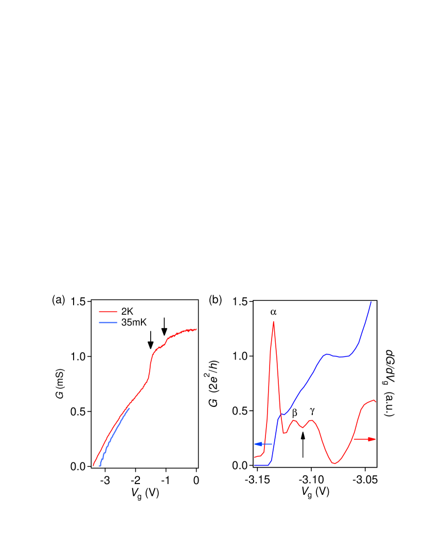
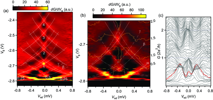
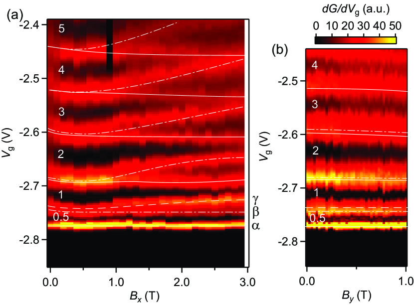
Figure 2 (a) shows as a function of at 2 K and 35 mK. Reflecting the property of double-layer systems at 2 K, drops twice at and V (indicated by the downward arrows), corresponding to the depletion of the front and back 2DEGs under the split gate, respectively. Then at 35 mK, several conductance plateaus are observed for V before the channel is pinched off at V. Figure 2 (b) shows detailed structures of and for . The resistances of the leads and at the contacts are subtracted accordingly. We observe a clear plateau in and a local minimum in the with a small plateau around (indicated by the upper arrow). The simultaneous observation of these two features for T has been reported in several experiments Nuttinck et al. (2000); Crook et al. (2006); Kohda et al. (2012); Rokhinson et al. (2006); Das et al. (2017). To the best of our knowledge, however, this has never been observed in a double-layer system before. To supplement the explanation, unlike the typical so-called “0.7 anomaly” in that a relatively higher temperature is required to observe a plateau-like feature Thomas et al. (1996), this minimum in is clearly observed at extremely low temperatures such as mK, indicating that it originates in a ground state. In addition, a 0.7 plateau is evolved into a clear 0.5 plateau by changing the electron density Thomas et al. (2000); Nuttinck et al. (2000); Reilly et al. (2001), or by increasing the in-plane magnetic field parallel to the channel Thomas et al. (1996). Therefore, the concurrent observation of 0.5 and 0.7 plateaus is rather unusual. Physically, the peaks observed in imply that the Fermi energy crosses the SBEs. In Fig. 2 (b), three peaks are shown between the and regions, suggesting that the Fermi energy crosses three SBEs in this region. We name these three peaks as , and from low to high .
Subsequently, the energy spectroscopy for the channel under the double-layer QPC was measured. Subband spacings of transverse modes at the QPC are observed in a spectroscopic measurement by controlling the Fermi energy through and the chemical potentials between the source and drain . Figure 3 (a) shows the image plot of as a function of and . The dark regions represent low ; therefore, these regions indicate plateau regions in the conductance, whereas the brighter regions represent high , indicating that a Fermi energy passes through an SBE. It is to be noted that the pinch-off voltage is different from that in Fig. 2 owing probably to unexpectedly localized electric charges. As compared to ordinary monolayer QPC cases Thomas et al. (1998); Kristensen et al. (2000); Cronenwett et al. (2002); Chen et al. (2010); Rössler et al. (2011), or even several tunnel-coupled double-layer QPC cases Salis et al. (1999); Fischer et al. (2006); Smith et al. (2009), the data reveal a rich SBE structure, particularly inside the first (lowest) SBE diamond (see also Fig. 3 (b), which is an enlarged image plot of Fig. 3 (a) around the first SBE structure). In Figs. 3 (a) and (b), we draw the SBE lines by connecting the maxima in on the image plot with the primary integer series in solid lines. The first large diamond appears from V and closes at V, with a width of approximately 1.5 mV. As is well known, this width is to determine the subband spacing in the QPC. The electrostatic potential at the narrow constriction can be described as a saddle point model Glazman et al. (1988); Büttiker (1990b); Lesovik and Sadovskyy (2011) given by
| (4) |
where is the electrostatic potential at the saddle, and the confinement potential curvatures are expressed in terms of the harmonic oscillation frequencies and . It is to be noted that our coordinate is different with that used in Ref. Büttiker, 1990b, in which the propagation direction is . The subband spacing in this diamond corresponds to meV. The observed diamond shapes resemble slightly crushed rhombuses as compared to those in previous reports (e.g., Kristensen et al. (2000)). Subsequently, we focus on the small structures by drawing split SBE lines in the result, using dash-dotted lines and a broken line. An enlarged image plot focusing on the structure in the first diamond is shown in Fig. 3 (b). From this experimental result, we observe three split SBE lines corresponding to the three peaks observed in Fig. 2 (b) (, and ) for the first-integer SBE. We will demonstrate that this SBE splitting is supported by the in-plane magnetic fields dependence of . Figure 3 (c) shows the profiles in units of as a function of . As shown, the conductance is asymmetric with respect to the positive and negative sides of . This asymmetry in is large below . As an example of the asymmetric behavior, we show a line profile of at V (the horizontal broken yellow line in Fig. 3 (b)) with a red curve in Fig. 3 (c). This asymmetric behavior was observed previously Kristensen et al. (2000), and explained in terms of self-gating effects. However, by analyzing the results of the shot noise measurements, which will be presented in Sec. III.2, we inferred that this asymmetry has an intrinsic physical origin.
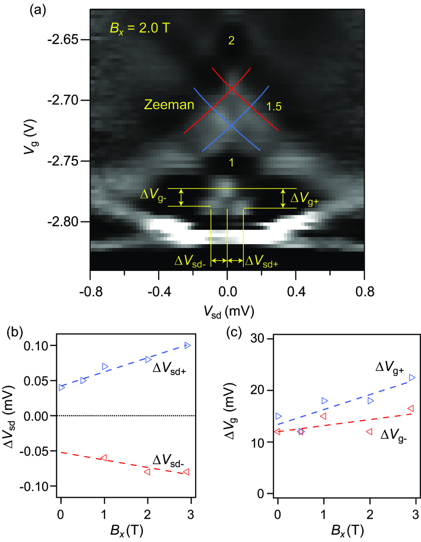
As we have explained in Sec. II, the in-plane components of the magnetic field, and , can be applied to the QPC independently. Figure 4 shows the image plots of as functions of (a) and , and (b) and . As is increased with T (fixed), each SBE except for the lowest SBE (marked with in Fig. 4 (a)) separates into two, then the upper branches move upwards. Even the SBE between the 0.5 and 1 plateaus decouples into two (marked with and ). Therefore, the SBE under the plateau splits into three, which is consistent with the observed SBE lines in Fig. 3. The other SBEs show a Zeeman splitting similar to the cases of monolayer QPCs Graham et al. (2008); Hew et al. (2008); Chen et al. (2008) as increases. It is remarkable that the SBE splitting starts at approximately T. However, as shown in Fig. 4 (b), the SBEs indicate no clear dependences on below 1 T; instead, they decrease slightly, particularly for higher SBEs. The lowest SBE shows no dependence of and . In addition, no clear onset of the second subladder (anti-symmetric wavefunction series) occurs for both in-plane fields below , contrary to the previous double-layer QPC data Thomas et al. (1999); Salis et al. (1999); Fischer et al. (2006).
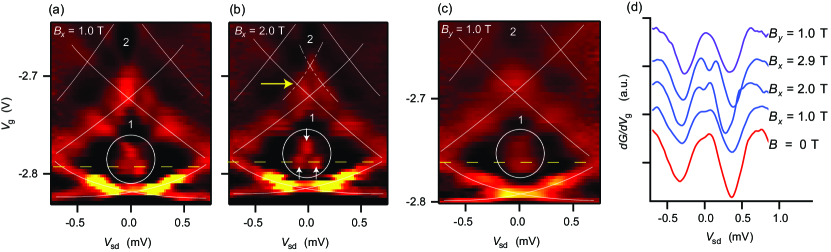
Figures 5 (a) through (c) show the image plots of for , 2.0 ( T), and T ( T), respectively. As increases, the structure in the first diamond (indicated by the white circles, SBE lines of and in Figs. 3 and 4) shows an interesting change. The lower broad peak separates into two peaks gradually, in contrast to the upper peak that becomes a clear single peak. This is demonstrated in Fig. 5 (b) ( T) as we indicate with three white arrows. Meanwhile, at T, each of the lower and upper peak smears out and becomes a broad peak. In Fig. 5 (d), we plot the profile of the lower peak at V (indicated by yellow broken lines in Figs. 5 (a) to (c)) at , and T. At T, a small shoulder appears on the left side of the center peak (at mV). However, we observe two peaks at and 2.9 T clearly, and at T slightly. Thus, the observed structure inside the first diamond shows a clear dependence on the magnitude of . Meanwhile, the higher SBE in Fig. 5 (b) (indicated by the yellow horizontal arrow at V) change differently; they exhibit a small diamond structure in accordance with the Zeeman gap opening as increases (see also Fig. 14 in Appendix B).
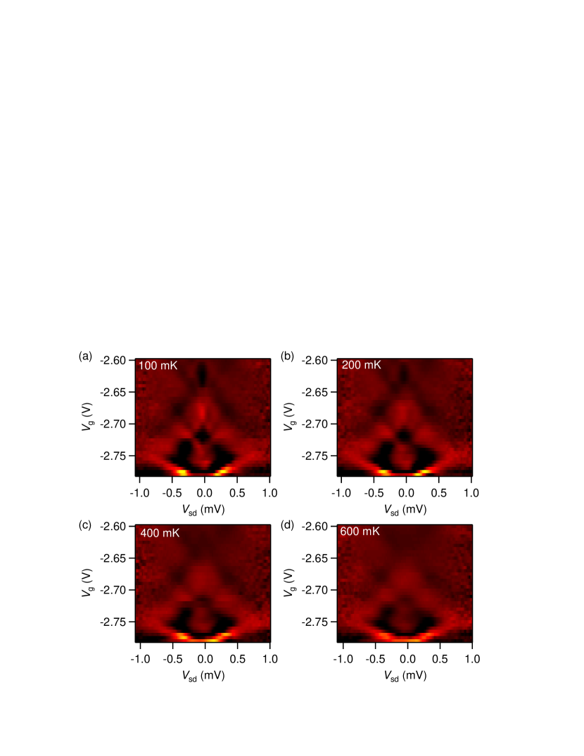
In addition, we observe a result that is different from the previous results of the 0.7 anomaly. Figure 6 shows the image plots of for several temperatures from 100 mK to 600 mK. Interestingly, the structure inside the first diamond smears out as is increased, showing a broad vague peak at the center of the diamond. Therefore, it is clear that the structure observed in this study originates from the band-dispersion of the double-layer system. Conversely, the minimum for plateau is robust. forms a clear plateau at ; after this plateau it increases without forming additional clear plateaus.
III.2 Results of the Shot Noise Measurement
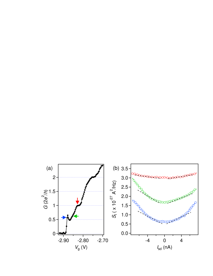
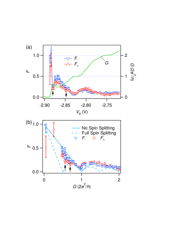
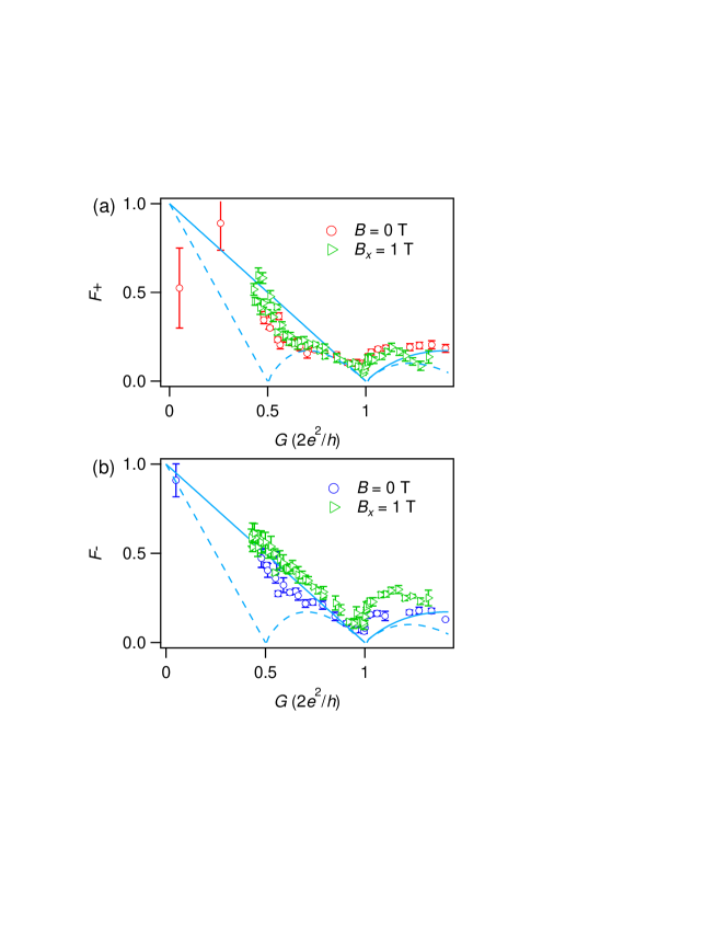
To further obtain information on the phenomenon from a different aspect, we performed shot noise measurements. Figure 7 (a) shows as a function of at 300 mK. The overshoot observed at the plateau is more prominent at higher temperatures, resembling the one observed in Sfigakis et al. (2008). We attribute the appearance of this overshoot to a resonance mode due to the superimposed transmission and reflection on the lowest SBE at the QPC region. Figure 7 (b) shows as a function of for , and V. shows a parabolic behavior for , and then shows a linear dependence for , which is a typical behavior of the shot noise with crossover from thermal noise to shot noise. We observe an asymmetric dependence between the positive and negative near , which was also observed previously Roche et al. (2004); Kristensen et al. (2000) and explained in terms of the self-gating effect in QPC. However, this asymmetry in is observed only for V (for ), and does not occur in other values, thus suggesting other possibilities. Accordingly, the slope of is always higher in the negative side of for . As we have stated earlier, we derived the Fano factor from the slope of as . Owing to the asymmetry between the positive and negative sides of the , we used the Fano factor of the positive side and negative side , and plotted them as a function of , as shown in Fig. 8 (a). Further, the zero bias () conductance is plotted on the right axis in Fig. 8 (a). Consistent with the result, is larger than between the and plateaus.
In a noninteracting scattering process, theory predictsBlanter and Büttiker (2000)
| (5) |
where denotes the transmission probability of the -th channel. We replot and as a function of in Fig. 8 (b), along with the theoretical value of when no spin splitting (the solid lines) and full spin splitting (the broken lines) occur. Both and are suppressed at and , thus implying the formation of a single perfect conductance channel in the coupled DQW for the plateau region. Two important features of and observed are 1) a clear suppression at and a rapid increase after this reduction as is decreased, and 2) a small reduction at (both reductions are indicated by the upper arrows in Fig. 8 (a) and (b)). Regarding the first point, the decrease in the Fano factor indicates that finishes crossing an SBE. After the suppression at , the Fano factor is increased even when the plateau of is established. Generally, the increase in the Fano factor indicates that a new conduction channel opens as increases from . The second point suggests that, as shown previously Roche et al. (2004); DiCarlo et al. (2006); Nakamura et al. (2009) regarding the 0.7 anomaly, the existing channels’ transmission probabilities contribute unequally to the conductance. This small reduction appears for both and . The values are larger than the theoretical values of at the conductance plateau region. For the enhanced Fano factor, three possibilities can be considered: electron heating Muro et al. (2016), channel mixing, and noise. However, the noise scarcely contribute to the enhancement in this experiment owing to the noise measurement technique using a high resonant frequency circuit and double-high electron mobility transistor amplifier Arakawa et al. (2013).
Furthermore, we measured the shot noise in the presence of in-plane magnetic fields. Fig. 9 shows and against for and T. In the presence of in-plane magnetic fields, the Fano factor increases. At T, the difference between and becomes larger than the zero field difference between the 0.5 and 1 plateau regions. As a notable difference, obeys the theoretical dependence well.
IV Discussion
In this section, first, we summarize our observations before presenting a discussion of the results. First, it is shown that three maxima exist inside the first diamond for the result, especially in the presence of a large . Next, , and exhibit an asymmetric dependence with respect to . However, in our results, an apparent beginning of the second layer SBE such as those observed in Refs. Thomas et al. (1999); Salis et al. (1999); Fischer et al. (2006) is not observed contrary to expectation. We cannot completely deny the possible effects from double-layer wavefunction mixing on the issues above. Thus, we must specify whether our observation originated from double-layer wavefunctions. Hence, we conducted computer simulations using the nextnano simulation software nex . The simulation results do not support the formation of double-layer wavefunctions; thus, it is difficult to explain the results solely based on double-layer effects. Having obtained the simulation results, we propose a possible explanation for the experimental results above using the spin effect, i.e., the SOI-modified dispersion relation in particular.
IV.1 Simulation Results
Because the system contains two layers (front and back), we must consider two subladders for the wavefunctions and confinement potentials. We denote the wavefunction of the system as
| (6) |
with direction for propagating modes, and directions and for lateral and vertical (quantum well) confinement, respectively. The envelope wavefunction can further be denoted as
| (7) |
where denotes the th lateral mode and denotes the th vertical wavefunction in the quantum well. For tunnel-coupled vertical modes,
| (8) |
where and denote the wavefunction in the front and back layers (subladder index), respectively, and denotes the interlayer phase difference. The index uses S or AS : for , for the symmetric bonding state, and for , for the anti-symmetric bonding state.
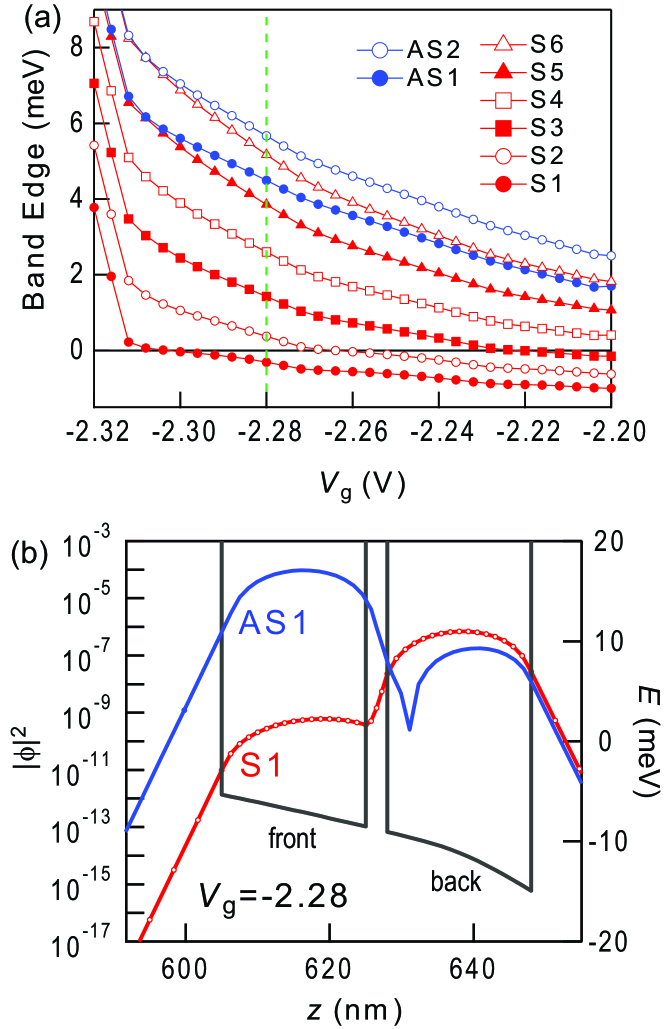
To confirm the SBEs in the first diamond, the wavefunction energies at the QPC were simulated using the self-consistent Schrödinger-Poisson method with nextnano. We first performed a one-dimensional (1D) simulation in the direction with reference to the characteristics of the bulk, i.e., the calculated and dependence of to determine the simulation parameters (see Appendix C). Subsequently, we proceeded with two-dimensional (2D) simulations in the plane as a function of . The SBE energies are calculated as the eigenvalues of the quantized wavefunctions in the plane under a lateral parabolic confinement potential. It is noteworthy that although the 2D simulation did not consider the direction, we assume that the -directional eigen-energies exhibit a qualitatively equivalent dependence on in the QPC region. Thus, the lateral potential and width are determined based on the value. Figure 10 (a) shows the SBE energies as a function of at the center of the QPC region. We found that the energy of the lowest anti-symmetric wavefunction () was higher than that of the fifth symmetric wavefunction (), because the screening effect of the front layer was extremely strong to allow for the electrons to realize the anti-symmetric wavefunction (hereinafter, we denote wavefunction using two indexes, and , such as AS1, because is always 1). In Fig. 10 (b), we show the of the lowest symmetric wavefunction (S1) and the anti-symmetric wavefunction (AS1) at the first plateau region. The wavefunction shows a large imbalance between the front and back layers, indicating an extremely weak coupling between the two layers under an applied strong electric field of approximately V/( m). Hence, we expect electrons to exist primarily in the back layer and their wavefunction to permeate to the front layer; thus, the system behaves as a single-layer system with a large potential gradient toward the front layer.
IV.2 Possible Explanation with SOI-induced Split Dispersion Relation
To explain the structure in the first diamond (indicated by the white circles in Fig. 5), the following simple relationship between the density of states (DOS) and conductivity can be useful. As is well known, the ballistic electron transport in a QPC shows the conductance that changes stepwise depending on the number of subbands below the Fermi level. Each subband carries the current
| (9) |
where denotes the 1D unidirectional density of states, and denotes the group velocity. Therefore, cancellation between the DOS and the Fermi velocity causes the conductance quantization. Equation (9) describes the importance of the DOS, because the conductance is the result of the integral of the current divided by the applied voltage. Experimentally, a sudden DOS change results in a large conductance jump and a large transconductance peak. In our experiment, the brighter the SBE in the plot, the larger are the DOS changes. Therefore, we observed three large DOS changes within the first diamond, as shown explicitly in Fig. 5 (b).
For the candidate of the threefold DOS change, we suggest the dispersion relation that splits in the wavenumber direction, such as the SOI-induced splitting Goulko et al. (2014); Quay et al. (2010); Kammhuber et al. (2017) and the in-plane magnetic-field-induced splitting for tunnel-coupled double-layer systems Lyo (1994), because three minima appear in the subbands. However, taking into account the simulation result, the possibility of realizing an in-plane magnetic-field-induced splitting is highly unlikely, because well-developed tunnel-coupled wavefunctions are a prerequisite for this to occur (we will discuss this in detail later). Regarding the SOI in this case, the space inversion symmetry is expected to be maintained for the and directions, but broken for the direction. Thus, the Rashba SOI Bychkov and Rashba (1984) with regard to the potential gradient in the direction and the current in the direction () is expected. The Hamiltonian regarding the Rashba SOI with this broken symmetry is
| (10) | ||||
| (11) |
where denotes the potential function of the DQW, denotes the component of the Pauli matrix, and is the so-called Rashba parameter. From Eq. (11) above, we can derive the dispersion relation with the Rashba SOI as
| (12) |
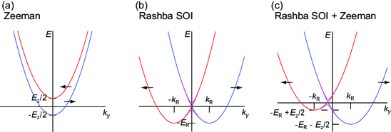
Then, the energy assumes a minimum value of at . Further, according to analysis Goulko et al. (2014); Quay et al. (2010), the -directional split subbands are mixed; consequently, the subbands repel and open a gap into the upper and lower branches (see Fig. 11 (b)). Importantly, the lower branch contains two minima and the upper branch contains one minimum, at which the up- and down-spin DOSs are degenerated; hence, this SOI-modified dispersion exhibits three large DOS changes. Furthermore, in the presence of , Eq. 12 is modified as follows:
| (13) |
where denotes the Bohr magneton. The dispersion relations of the Zeeman splitting, Rashba SOI splitting, and Rashba SOI plus Zeeman splitting cases are illustrated in Fig. 11. The Rashba parameter should be modified because of an additional magnetic confinement potential created by , Salis et al. (1999) () in the plane, as follows:
| (14) |
Thus, the Rashba energy increases with the increase in , which is a magnetic field parallel to the Rashba SOI field. This indicates that the two minima in the dispersion curves of Rashba SOI separate with the increase in ; further, the crossing point and a side of a minimum separate vertically, whereas the other side approaches. As shown in Fig. 5, the lower two maxima inside the first diamond separate as increases, and thus agree qualitatively to the behavior of minima in the dispersion curves of Rashba SOI.
We extract the positions of the lower two maxima as and . In addition, the separation of the center maximum and each lower maximum is extracted as and (see Fig. 12 (a) for graphical illustration). Figure 12 (b) and (c) show the and the values, respectively, as a function of . Although increases slightly, the overall changes correspond well to the three points in the dispersion curves of the Rashba SOI plus Zeeman splitting—the crossing point and the two minima. Therefore, the three maxima observed inside the first diamond can be attributed to these points. Considering that the Rashba SOI field is proportional to , the principle behind the observed SOI is simple: the strong potential gradient and high mobility (or the large relaxation time Edelstein (1990)) of the sample. In our opinion, the center barrier in the DQW produces this strong potential gradient, as shown in the potential profile in Fig. 10 (b).
Furthermore, the shot noise results support the conjecture above in that the SBE splitting originates from the SOI. As shown in Fig. 9, the additional increases to theoretical values. In addition, the difference between and becomes larger at T. Given that is in the same direction as that of the effective Rashba magnetic field , when the current flows from the source to drain, (hence the electron momentum is in the opposite direction), a positive supports . However, the situation is completely different when is negative, because a positive cancels as is induced to the negative direction. Therefore, in the presence of the positive , the separation by the Rashba SOI is enhanced for and decreased for . Consequently, is suppressed for and hence , and vice versa. As shown in Fig. 8, this anisotropic Fano factor is observed at 0 T. This is attributed to the effective Zeeman energy .
An alternative SOI-like dispersion splitting can be considered in a tunnel-coupled double-layer system. According to Ref Lyo (1994), an in-plane field induces the subband splitting in proportional to the magnitude of the in-plane field in the direction perpendicular to the in-plane field for 2DEG systems. Thus, splits the subband in the direction as . However, the estimated separation for T is m-1, thus yielding meV. Although the theory considers a double-layer 2DEG system, this value is significantly large, comparable to the observed first diamond splitting. Furthermore, we cannot explain the small split that is already observed at the zero magnetic field. In addition, a strong double-layer coupling is a prerequisite for this splitting. As shown in Fig. 10 (b), the wavefunctions in the lower subbands are the highly unbalanced bonding state. Therefore, this cannot be the primary contribution to the horizontal splitting.
Finally, we would like to briefly discuss the reentrant conductance behavior that was observed in strong SOI systems in previous studies Quay et al. (2010); Kammhuber et al. (2017); Heedt et al. (2017). In this study, a small reentrant feature was confirmed as shown in Fig. 2 (b), and in the conductance data in Fig. 7 and 8, although we interpreted them as a resonant mode. However, these features are not apparent compared with those in Ref.Quay et al. (2010); Kammhuber et al. (2017); Heedt et al. (2017). We attribute this to the band structure of the sample: the second lowest band exists immediately above the lowest band. This configuration suppresses “the helical gap” and obscures the reentrant behavior.
V Concluding Remarks and Perspectives
We herein have revealed the SBE lines as a consequence of the wavenumber direction subband splitting induced by a strong SOI. We have observed the coexistence of a 0.5 plateau and a structure at 0.7 in a double-layer QPC system. The structure observed in the spectroscopy has revealed three maxima corresponding to the three minima in the dispersion relation of the wavenumber-directional subband splitting. We attribute this splitting to a strong SOI owing to the high potential gradient at the center barrier and the high mobility of the double-layer sample. The Fano factor obtained from the shot noise measurement have indicated an asymmetric transmission probability. This result further supports the SOI-modified dispersion model and the asymmetry observed in the conductance measurement. However, multiple unanswered questions still exist that require theoretical considerations and additional experiments. This experiment includes useful information on spintronics and quantum engineering that would benefit applications. In particular, a strong SOI in a GaAs/AlGaAs sample invokes spintronic applications in this well-developed platform. In addition, we intend to perform shot noise measurements in the QHE region of this system in the future.
Appendix A Shubnikov de-Haas Oscillation Analysis
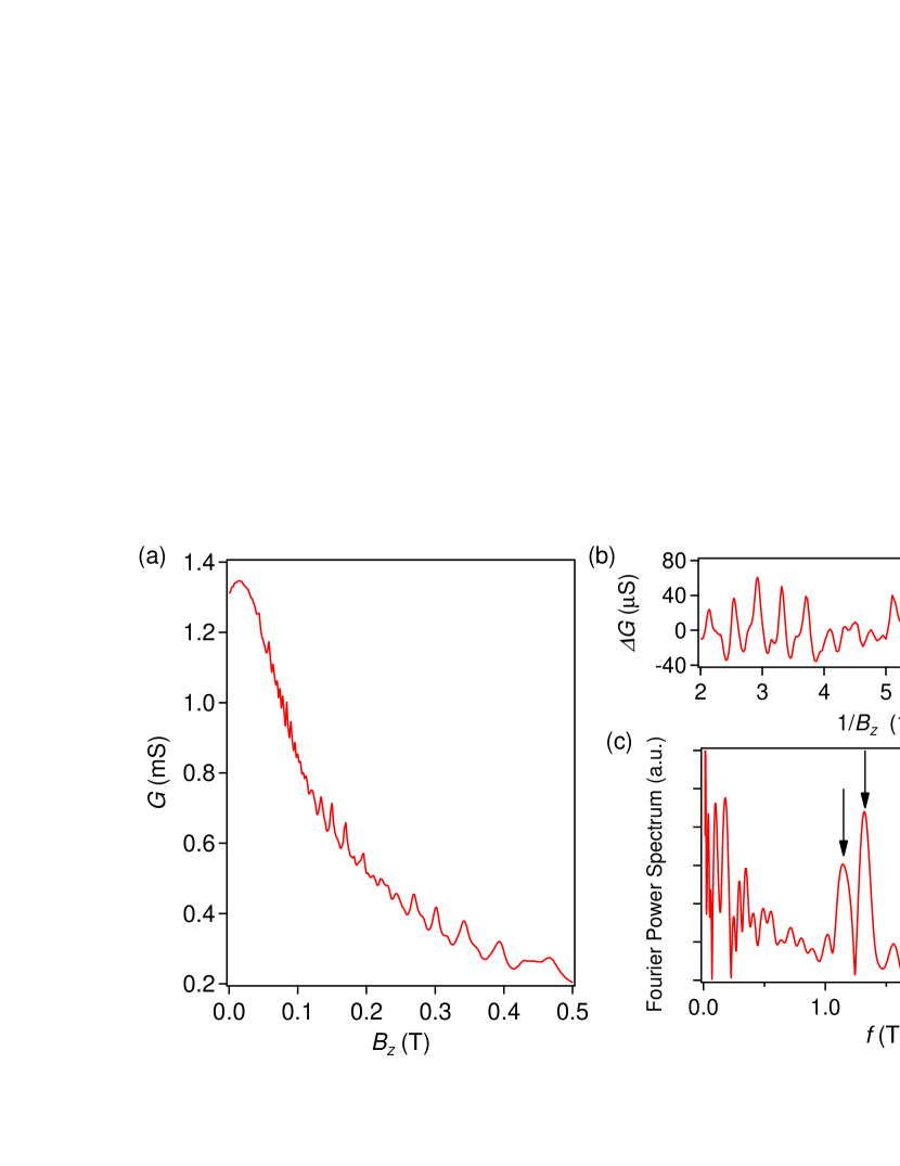
First, we measure the Shubnikov de-Haas (SdH) oscillation at zero bias () and zero split gate voltages () in low magnetic fields at the lowest temperature available in this experiment, to obtain the electron densities and tunnel coupling strength between the layers. Figure 13 (a) shows as a function of . As a clear sign of the weak localization effect Bergmann (1984), positive magneto-conductance is observed initially. Subsequently, the difference in density between the symmetric state and anti-symmetric state results in a beating of the SdH oscillations in Boebinger et al. (1991). This beating is resolved into two sharp peaks of Fourier power spectrum from the fast Fourier transform analysis of the dependence of , as shown in Fig. 13 (c) by the arrows. The density corresponding to each peak is, as we mentioned earlier, and cm-2 from a well-known relation between the SdH frequency and , , and the energy separation between the symmetric and anti-symmetric states is meV, where in GaAs with denotes the electron rest mass, and and denotes the electron density in the symmetric and anti-symmetric states, respectively.
Appendix B Supplemental Data
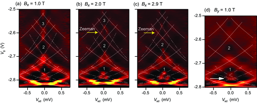
Figures 14 (a) through (d) show the overall view of the image plots of as a function of and for T and T, respectively. For and 2.9 T, the spin degeneracy is resolved for higher SBEs; consequently, we observe a minimum (dark region) corresponding to the plateau (indicated by yellow arrows). From this gap opening, the Zeeman splitting is meV at T. Compared to the bare -factor of GaAs (), the Zeeman energy, , at this in-plane magnetic field is approximately twice that of the bare Zeeman splitting.
Appendix C Computer simulation using nextnano software
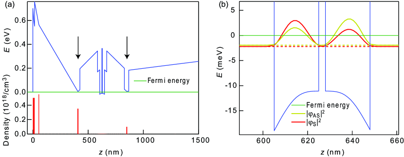
To estimate the double-layer effects on the conductance, we must calculate the wavefunctions at the double-layer QPC under a strong electric field confinement. Hence, we used the electronic simulator software, nextnano nex . To supplement the main text, we provide the 1D simulation results of the calculation and the dependence of the wavefunctions. Figure 15 (a) shows the potential profile for the direction and the electron density profile. Owing to our careful design, two Si -doping positions, indicated by the two downward arrows, render the DQW symmetric against the direction successfully. Fig. 15 (b) shows the energy of symmetric and anti-symmetric wavefunctions and their probability density profiles at V. The tunnel gap, , is calculated as 0.25 meV, which is extremely close to the experimental value. We tabulate the measured and calculated values of in Table 2, along with the densities of the lowest symmetric and anti-symmetric wavefunctions.
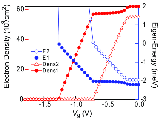
Figure 16 shows the calculated eigen-energies from the 1D simulation (-direction) for the lowest wavefunction and the electron density for each layer as a function of . As increases in the negative direction, the potential of the front layer increases, the symmetric state electrons depopulate from the front layer, and the energy separation between the symmetric and anti-symmetric wavefunctions becomes larger. As shown in Fig. 2 (a), drops twice at the two downward arrows. Although these two points represent two pinch-off points in the bulk 2DEGs of the front and back layers under the m-scale gate electrodes, we assume that the calculation results above correspond to this behavior.
| Experiment | Calculation | |
|---|---|---|
| () | 6.4 | 6.2 |
| () | 5.6 | 5.5 |
| (mV) | 0.29 | 0.25 |
Acknowledgements.
We are grateful to K. Muraki and T. Saku of the NTT basic research laboratories and A. Sawada for providing us with a high mobility sample, and to M. Hashisaka and A. Ueda for their productive discussion. This work was supported by the JSPS KAKENHI (JP15K17680, JP15H05854, JP18H01815, JP19H05826, JP19H00656).References
- van Wees et al. (1988) B. J. van Wees, H. van Houten, C. W. J. Beenakker, J. G. Williamson, L. P. Kouwenhoven, D. van der Marel, and C. T. Foxon, Quantized conductance of point contacts in a two-dimensional electron gas, Phys. Rev. Lett. 60, 848 (1988).
- Wharam et al. (1988) D. A. Wharam, T. J. Thornton, R. Newbury, M. Pepper, H. Ahmed, J. E. F. Frost, D. G. Hasko, D. C. Peacock, D. A. Ritchie, and G. A. C. Jones, One-dimensional transport and the quantisation of the ballistic resistance, Journal of Physics C: Solid State Physics 21, L209 (1988).
- Thomas et al. (1996) K. J. Thomas, J. T. Nicholls, M. Y. Simmons, M. Pepper, D. R. Mace, and D. A. Ritchie, Possible spin polarization in a one-dimensional electron gas, Phys. Rev. Lett. 77, 135 (1996).
- Landauer (1957) R. Landauer, Spatial variation of currents and fields due to localized scatterers in metallic conduction, IBM Journal of Research and Development 1, 223 (1957).
- Büttiker (1986) M. Büttiker, Four-terminal phase-coherent conductance, Phys. Rev. Lett. 57, 1761 (1986).
- Büttiker et al. (1985) M. Büttiker, Y. Imry, R. Landauer, and S. Pinhas, Generalized many-channel conductance formula with application to small rings, Phys. Rev. B 31, 6207 (1985).
- Bruus et al. (2001) H. Bruus, V. V. Cheianov, and K. Flensberg, The anomalous 0.5 and 0.7 conductance plateaus in quantum point contacts, Physica E 10, 97 (2001).
- Reilly et al. (2001) D. J. Reilly, G. R. Facer, A. S. Dzurak, B. E. Kane, R. G. Clark, P. J. Stiles, R. G. Clark, A. R. Hamilton, J. L. O’Brien, N. E. Lumpkin, L. N. Pfeiffer, and K. W. West, Many-body spin-related phenomena in ultra low-disorder quantum wires, Phys. Rev. B 63, 121311(R) (2001).
- Wang and Berggren (1998) C.-K. Wang and K.-F. Berggren, Local spin polarization in ballistic quantum point contacts, Phys. Rev. B 57, 4552 (1998).
- Daul and Noack (1998) S. Daul and R. M. Noack, Ferromagnetic transition and phase diagram of the one-dimensional hubbard model with next-nearest-neighbor hopping, Phys. Rev. B 58, 2635 (1998).
- Yang (2004) K. Yang, Ferromagnetic transition in one-dimensional itinerant electron systems, Phys. Rev. Lett. 93, 066401 (2004).
- Micolich (2011) A. P. Micolich, What lurks below the last plateau: experimental studies of the conductance anomaly in one-dimensional systems, Journal of Physics: Condensed Matter 23, 443201 (2011).
- Büttiker (1990a) M. Büttiker, Scattering theory of thermal and excess noise in open conductors, Phys. Rev. Lett. 65, 2901 (1990a).
- Büttiker (1992) M. Büttiker, Scattering theory of current and intensity noise correlations in conductors and wave guides, Phys. Rev. B 46, 12485 (1992).
- Lesovik (1989) G. B. Lesovik, Excess quantum noise in 2d ballistic point contacts, JETP Lett. 49, 592 (1989).
- Yurke and Kochanski (1990) B. Yurke and G. P. Kochanski, Momentum noise in vacuum tunneling transducers, Phys. Rev. B 41, 8184 (1990).
- Martin and Landauer (1992) T. Martin and R. Landauer, Wave-packet approach to noise in multichannel mesoscopic systems, Phys. Rev. B 45, 1742 (1992).
- Blanter and Büttiker (2000) Y. Blanter and M. Büttiker, Shot noise in mesoscopic conductors, Physics Reports 336, 1 (2000).
- Kobayashi (2016) K. Kobayashi, What can we learn from noise ? —mesoscopic nonequilibrium statistical physics—, Proc. Jpn. Acad., Ser. B 92, 204 (2016).
- Kumar et al. (1996) A. Kumar, L. Saminadayar, D. C. Glattli, Y. Jin, and B. Etienne, Experimental test of the quantum shot noise reduction theory, Phys. Rev. Lett. 76, 2778 (1996).
- Reznikov et al. (1995) M. Reznikov, M. Heiblum, H. Shtrikman, and D. Mahalu, Temporal correlation of electrons: Suppression of shot noise in a ballistic quantum point contact, Phys. Rev. Lett. 75, 3340 (1995).
- Roche et al. (2004) P. Roche, J. Ségala, D. C. Glattli, J. T. Nicholls, M. Pepper, A. C. Graham, K. J. Thomas, M. Y. Simmons, and D. A. Ritchie, Fano factor reduction on the 0.7 conductance structure of a ballistic one-dimensional wire, Phys. Rev. Lett. 93, 116602 (2004).
- DiCarlo et al. (2006) L. DiCarlo, Y. Zhang, D. T. McClure, D. J. Reilly, C. M. Marcus, L. N. Pfeiffer, and K. W. West, Shot-noise signatures of 0.7 structure and spin in a quantum point contact, Phys. Rev. Lett. 97, 036810 (2006).
- Gershon et al. (2008) G. Gershon, Y. Bomze, E. V. Sukhorukov, and M. Reznikov, Detection of non-gaussian fluctuations in a quantum point contact, Phys. Rev. Lett. 101, 016803 (2008).
- Hashisaka et al. (2008) M. Hashisaka, Y. Yamauchi, S. Nakamura, S. Kasai, T. Ono, and K. Kobayashi, Bolometric detection of quantum shot noise in coupled mesoscopic systems, Phys. Rev. B 78, 241303(R) (2008).
- Nakamura et al. (2009) S. Nakamura, M. Hashisaka, Y. Yamauchi, S. Kasai, T. Ono, and K. Kobayashi, Conductance anomaly and fano factor reduction in quantum point contacts, Phys. Rev. B 79, 201308(R) (2009).
- Kohda et al. (2012) M. Kohda, S. Nakamura, Y. Nishihara, K. Kobayashi, T. Ono, J. Ohe, Y. Tokura, T. Mineno, and J. Nitta, Spin-orbit induced electronic spin separation in semiconductor nanostructures, Nature Communications 3, 1082 (2012).
- Wolf et al. (2001) S. Wolf, D. Awschalom, R. Buhrman, J. Daughton, S. von Molnár, M. Roukes, A. Chtchelkanova, and D. Treger, Spintronics: A spin-based electronics vision for the future, Science 294, 1488 (2001).
- Awschalom and Flatté (2007) D. D. Awschalom and M. E. Flatté, Challenges for semiconductor spintronics, Nat. Phys. 3, 153 (2007).
- Bennett and DiVincenzo (2000) C. H. Bennett and D. P. DiVincenzo, Quantum information and computation, Nature 404, 247 (2000).
- Bielejec et al. (2005) E. Bielejec, J. A. Seamons, J. L. Reno, and M. P. Lilly, Tunneling and nonlinear transport in a vertically coupled gaas/algaas double quantum wire system, Appl. Phys. Lett. 86, 083101 (2005).
- Bertoni et al. (2000) A. Bertoni, P. Bordone, R. Brunetti, C. Jacoboni, and S. Reggiani, Quantum logic gates based on coherent electron transport in quantum wires, Phys. Rev. Lett. 84, 5912 (2000).
- Ramamoorthy et al. (2007) A. Ramamoorthy, J. P. Bird, and J. L. Reno, Using split-gate structures to explore the implementation of a coupled-electron-waveguide qubit scheme, J. Phys.: Condens. Matter 19, 276205 (2007).
- Thomas et al. (1999) K. J. Thomas, J. T. Nicholls, M. Y. Simmons, W. R. Tribe, A. G. Davies, and M. Pepper, Controlled wave-function mixing in strongly coupled one-dimensional wires, Phys. Rev. B 59, 12252 (1999).
- Salis et al. (1999) G. Salis, T. Heinzel, K. Ensslin, O. J. Homan, W. Bächtold, K. Maranowski, and A. C. Gossard, Mode spectroscopy and level coupling in ballistic electron waveguides, Phys. Rev. B 60, 7756 (1999).
- Thomas et al. (2000) K. J. Thomas, J. T. Nicholls, M. Pepper, W. R. Tribe, M. Y. Simmons, and D. A. Ritchie, Spin properties of low-density one-dimensional wires, Phys. Rev. B 61, R13365 (2000).
- Nuttinck et al. (2000) S. Nuttinck, K. Hashimoto, S. Miyashita, T. Saku, Y. Yamamoto, and Y. Hirayama, Quantum point contacts in a density-tunable two-dimensional electron gas, Jpn. J. Appl. Phys. 39, L655 (2000).
- Fischer et al. (2006) S. F. Fischer, G. Apetrii, U. Kunze, D. Schuh, and G. Abstreiter, Energy spectroscopy of controlled coupled quantum-wire states, Nature Phys. 2, 91 (2006).
- Smith et al. (2009) L. W. Smith, W. K. Hew, K. J. Thomas, M. Pepper, I. Farrer, D. Anderson, G. A. C. Jones, and D. A. Ritchie, Row coupling in an interacting quasi-one-dimensional quantum wire investigated using transport measurements, Phys. Rev. B 80, 041306(R) (2009).
- Ichinokura et al. (2013) S. Ichinokura, H. Hatano, W. Izumida, K. Nagase, and Y. Hirayama, Electrical control of tunnel coupling between vertically coupled quantum point contacts, Appl. Phys. Lett. 103, 062106 (2013).
- Datta and Das (1990) S. Datta and B. Das, Electronic analog of the electro‐optic modulator, Appl. Phys. Lett. 56, 665 (1990).
- Nichele et al. (2015) F. Nichele, S. Hennel, P. Pietsch, W. Wegscheider, P. Stano, P. Jacquod, T. Ihn, and K. Ensslin, Generation and detection of spin currents in semiconductor nanostructures with strong spin-orbit interaction, Phys. Rev. Lett. 114, 206601 (2015).
- Quay et al. (2010) C. H. L. Quay, T. L. Hughes, J. A. Sulpizio, L. N. Pfeiffer, K. W. Baldwin, K. W. West, D. Goldhaber-Gordon, and R. de Picciotto, Observation of a one-dimensional spin-orbit gap in a quantum wire, Nat. Phys. 6, 336 (2010).
- Kammhuber et al. (2017) J. Kammhuber, M. C. Cassidy, F. Pei, M. P. Nowak, A. Vuik, O. Gül, D. Car, S. R. Plissard, E. P. A. M. Bakkers, M. Wimmer, and L. P. Kouwenhoven, Conductance through a helical state in an indium antimonide nanowire, Nature Communications 8, 478 (2017).
- Heedt et al. (2017) S. Heedt, N. Traverso Ziani, F. Crépin, W. Prost, S. Trellenkamp, J. Schubert, D. Grützmacher, B. Trauzettel, and T. Schäpers, Signatures of interaction-induced helical gaps in nanowire quantum point contacts, Nat. Phys. 13, 563 (2017).
- Srinivasan et al. (2017) A. Srinivasan, D. S. Miserev, K. L. Hudson, O. Klochan, K. Muraki, Y. Hirayama, D. Reuter, A. D. Wieck, O. P. Sushkov, and A. R. Hamilton, Detection and control of spin-orbit interactions in a hole quantum point contact, Phys. Rev. Lett. 118, 146801 (2017).
- Masuda et al. (2018) T. Masuda, K. Sekine, K. Nagase, K. S. Wickramasinghe, T. D. Mishima, M. B. Santos, and Y. Hirayama, Transport characteristics of insb trench-type in-plane gate quantum point contact, Appl. Phys. Lett. 112, 192103 (2018).
- Ferrier et al. (2016) M. Ferrier, T. Arakawa, T. Hata, R. Fujiwara, R. Delagrange, R. Weil, R. Deblock, R. Sakano, A. Oguri, and K. Kobayashi, Universality of non-equilibrium fluctuations in strongly correlated quantum liquids, Nat. Phys. 12, 230 (2016).
- Crook et al. (2006) R. Crook, J. Prance, K. J. Thomas, S. J. Chorley, I. Farrer, D. A. Ritchie, M. Pepper, and C. G. Smith, Conductance quantization at a half-integer plateau in a symmetric gaas quantum wire, Science 312, 1359 (2006).
- Debray et al. (2009) P. Debray, S. M. S. Rahman, J. Wan, R. S. Newrock, M. Cahay, A. T. Ngo, S. E. Ulloa, S. T. Herbert, M. Muhammad, and M. Johnson, All-electric quantum point contact spin-polarizer, Nature Nanotech. 4, 759 (2009).
- Das et al. (2017) P. P. Das, A. Jones, M. Cahay, S. Kalita, S. S. Mal, N. S. Sterin, T. R. Yadunath, M. Advaitha, and S. T. Herbert, Dependence of the conductance plateau on the aspect ratio of quantum point contacts with in-plane side gates, J. Appl. Phys. 121, 083901 (2017).
- Bychkov and Rashba (1984) Y. Bychkov and E. Rashba, Properties of a 2d electron gas with lifted spectral degeneracy, JETP Lett. 39, 78 (1984).
- Nishihara et al. (2012) Y. Nishihara, S. Nakamura, K. Kobayashi, T. Ono, M. Kohda, and J. Nitta, Shot noise suppression in / quantum channels, Appl. Phys. Lett. 100, 203111 (2012).
- Arakawa et al. (2013) T. Arakawa, Y. Nishihara, M. Maeda, S. Norimoto, and K. Kobayashi, Cryogenic amplifier for shot noise measurement at 20 mk, Appl. Phys. Lett. 103, 172104 (2013).
- Muro et al. (2016) T. Muro, Y. Nishihara, S. Norimoto, M. Ferrier, T. Arakawa, K. Kobayashi, T. Ihn, C. Rössler, K. Ensslin, C. Reichl, and W. Wegscheider, Finite shot noise and electron heating at quantized conductance in high-mobility quantum point contacts, Phys. Rev. B 93, 195411 (2016).
- Rokhinson et al. (2006) L. P. Rokhinson, L. N. Pfeiffer, and K. W. West, Spontaneous spin polarization in quantum point contacts, Phys. Rev. Lett. 96, 156602 (2006).
- Thomas et al. (1998) K. J. Thomas, J. T. Nicholls, N. J. Appleyard, M. Y. Simmons, M. Pepper, D. R. Mace, W. R. Tribe, and D. A. Ritchie, Interaction effects in a one-dimensional constriction, Phys. Rev. B 58, 4846 (1998).
- Kristensen et al. (2000) A. Kristensen, H. Bruus, A. E. Hansen, J. B. Jensen, P. E. Lindelof, C. J. Marckmann, J. Nygård, C. B. Sørensen, F. Beuscher, A. Forchel, and M. Michel, Bias and temperature dependence of the 0.7 conductance anomaly in quantum point contacts, Phys. Rev. B 62, 10950 (2000).
- Cronenwett et al. (2002) S. M. Cronenwett, H. J. Lynch, D. Goldhaber-Gordon, L. P. Kouwenhoven, C. M. Marcus, K. Hirose, N. S. Wingreen, and V. Umansky, Low-temperature fate of the 0.7 structure in a point contact: A kondo-like correlated state in an open system, Phys. Rev. Lett. 88, 226805 (2002).
- Chen et al. (2010) T.-M. Chen, A. C. Graham, M. Pepper, I. Farrer, D. Anderson, G. A. C. Jones, and D. A. Ritchie, Direct observation of nonequilibrium spin population in quasi-one-dimensional nanostructures, Nano Lett. 10, 2330 (2010).
- Rössler et al. (2011) C. Rössler, S. Baer, E. de Wiljes, P.-L. Ardelt, T. Ihn, K. Ensslin, C. Reichl, and W. Wegscheider, Transport properties of clean quantum point contacts, New Journal of Physics 13, 113006 (2011).
- Glazman et al. (1988) L. I. Glazman, G. B. Lesovik, D. E. Khmel’nitskii, and R. I. Shekhter, Reflectionless quantum transport and fundamental ballistic-resistance steps in microscopic constrictions, JETP Lett. 48, 238 (1988).
- Büttiker (1990b) M. Büttiker, Quantized transmission of a saddle-point constriction, Phys. Rev. B 41, 7906 (1990b).
- Lesovik and Sadovskyy (2011) G. B. Lesovik and I. A. Sadovskyy, Scattering matrix approach to the description of quantum electron transport, Physics-Uspekhi 54, 1007 (2011).
- Graham et al. (2008) A. C. Graham, M. Y. Simmons, D. A. Ritchie, and M. Pepper, Anticrossing of spin-split subbands in quasi-one-dimensional wires, Phys. Rev. Lett. 100, 226804 (2008).
- Hew et al. (2008) W. K. Hew, K. J. Thomas, M. Pepper, I. Farrer, D. Anderson, G. A. C. Jones, and D. A. Ritchie, Spin-incoherent transport in quantum wires, Phys. Rev. Lett. 101, 036801 (2008).
- Chen et al. (2008) T.-M. Chen, A. C. Graham, M. Pepper, I. Farrer, and D. A. Ritchie, Bias-controlled spin polarization in quantum wires, Appl. Phys. Lett. 93, 032102 (2008).
- Sfigakis et al. (2008) F. Sfigakis, C. J. B. Ford, M. Pepper, M. Kataoka, D. A. Ritchie, and M. Y. Simmons, Kondo effect from a tunable bound state within a quantum wire, Phys. Rev. Lett. 100, 026807 (2008).
- (69) URL: https://www.nextnano.de.
- Goulko et al. (2014) O. Goulko, F. Bauer, J. Heyder, and J. von Delft, Effect of spin-orbit interactions on the 0.7 anomaly in quantum point contacts, Phys. Rev. Lett. 113, 266402 (2014).
- Lyo (1994) S. K. Lyo, Transport and level anticrossing in strongly coupled double quantum wells with in-plane magnetic fields, Phys. Rev. B 50, 4965 (1994).
- Edelstein (1990) V. Edelstein, Spin polarization of conduction electrons induced by electric current in two-dimensional asymmetric electron systems, Solid State Commun. 73, 233 (1990).
- Bergmann (1984) G. Bergmann, Weak localization in thin films: a time-of-flight experiment with conduction electrons, Phys. Rep. 107, 1 (1984).
- Boebinger et al. (1991) G. S. Boebinger, A. Passner, L. N. Pfeiffer, and K. W. West, Measurement of fermi-surface distortion in double quantum wells from in-plane magnetic fields, Phys. Rev. B 43, 12673 (1991).