Spin-dependent transport through the Weyl semimetal surface
Abstract
We experimentally compare two types of interface structures with magnetic and non-magnetic Weyl semimetals. They are the junctions between a gold normal layer and magnetic Weyl semimetal Ti2MnAl, and a ferromagnetic nickel layer and non-magnetic Weyl semimetal WTe2, respectively. Due to the ferromagnetic side of the junction, we investigate spin-polarized transport through the Weyl semimetal surface. For both structures, we demonstrate similar current-voltage characteristics, with hysteresis at low currents and sharp peaks in differential resistance at high ones. Despite this behavior resembles the known current-induced magnetization dynamics in ferromagnetic structures, evolution of the resistance peaks with magnetic field is unusual. We connect the observed effects with current-induced spin dynamics in Weyl topological surface states.
pacs:
73.40.Qv 71.30.+hI Introduction
Recent interest to topological semimetals is connected with their peculiar properties armitage , which originates from gapless spectrum with band touching in some distinct points. In Weyl semimetals (WSM) every touching point splits into two Weyl nodes with opposite chiralities due to the time reversal or inversion symmetries breaking. The projections of two Weyl nodes on the surface Brillouin zone are connected by a Fermi arc, which represents the topologically protected surface state armitage . Most of experimentally investigated WSMs, were non-centrosymmetric crystals with broken inversion symmetry armitage . For example, spin- and angle- resolved photoemission spectroscopy data indeed demonstrate spin-polarized surface Fermi arcs das16 ; feng2016 for a WTe2 Weyl semimetal li2017 ; soluyanov . In contrast, there are only a few candidates of magnetically ordered materials for the realization of WSMs mag1 ; mag2 ; mag3 ; mag4 ; kagome ; kagome1 .
Ti2MnAl is one of the newly predicted timnal ; timnal_review magnetic WSM. The bulk Ti2MnAl is a spin gapless semiconductor, where the valence and conduction bands touch each other in the spin-up channel and there is a large gap in the spin down band structure timnal_exp . Therefore, the bulk Ti2MnAl has 100% spin polarized carriers.
It is well known, that the magnetically ordered materials allows complicated magnetization dynamics. For example, current-induced excitation of spin waves, or magnons, was demonstrated as sharp differential resistance peaks in ferromagnetic multilayers at large electrical current densities myers ; tsoi1 ; tsoi2 ; katine ; single ; balkashin ; balashov . In these structures, spin-dependent scattering may even reverse the magnetic moments of the layers, which results in switchings at low currents, accomplished by well-defined hysteresis myers .
Bulk magnons were also demonstrated cosns for magnetic WSM at low current densities due to the coupling between two magnetic moments mediated by Weyl fermions weyl_magnon . Also, in a bilayer consisting of a magnetic WSM and a normal metal, a charge current can be induced in the WSM by spin current injection at the interface bilayer . On the other hand, there are spin-polarized surface Fermi arcs on a WSM surface das16 ; feng2016 ; jiang15 ; rhodes15 ; wang16 . Similarly to the case of topological insulators topinssurf , one can expect current-induced magnetization dynamics current also for surface magnetic textures texture ; araki in WSM.
Here, we experimentally compare two types of interface structures with magnetic and non-magnetic Weyl semimetals. They are the junctions between a gold normal layer and magnetic Weyl semimetal Ti2MnAl, and a ferromagnetic nickel layer and non-magnetic Weyl semimetal WTe2, respectively. Due to the ferromagnetic side of the junction, we investigate spin-polarized transport through the Weyl semimetal surface. For both structures, we demonstrate similar current-voltage characteristics, with hysteresis at low currents and sharp peaks in differential resistance at high ones. Despite this behavior resembles the known current-induced magnetization dynamics in ferromagnetic structures, evolution of the resistance peaks with magnetic field is unusual. We connect the observed effects with current-induced spin dynamics in Weyl topological surface states.
II Samples and technique
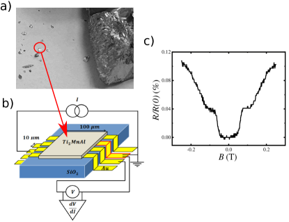
Ti2MnAl was obtained as a bulk ingot by levitation melting in high-frequency (60-70 kHz) induction furnace. A mixture of Mn and Al powders was placed into the cylindrical titanium capsule and melted in a suspended condition for 20 minutes in argon medium at 0.2 MPa pressure and at 2080 K temperature. After switching the heater off the resulting globule of the melt was dropped to a cooled copper crystallizer, where it was quenched at 278 K. The ingot cleaved mechanically for further processing as shown in Fig. 1 (a) and (b). We check by standard magnetoresistance measurements that our Ti2MnAl is characterized by low positive magnetiresistance, see Fig. 1 (c), which has been demonstrated for this material timnal_exp .
WTe2 compound was synthesized from elements by reaction of metal with tellurium vapor in the sealed silica ampule. The WTe2 crystals were grown by the two-stage iodine transport growth1 , that previously was successfully applied growth1 ; growth2 for growth of other metal chalcogenides like NbS2 and CrNb3S6. The WTe2 composition is verified by energy-dispersive X-ray spectroscopy. The X-ray diffraction (Oxford diffraction Gemini-A, MoK) confirms orthorhombic single crystal WTe2 with lattice parameters Å, Å, and Å. We check that our WTe2 crystals demonstrate large (about 3000%), non-saturating positive magnetoresistance up to 14 T field, as it has been shown ali2014 ; lvEPL15 for WTe2 and is expected jiang15 ; rhodes15 ; wang16 for non-magnetic type-II Weyl semimetals li2017 .
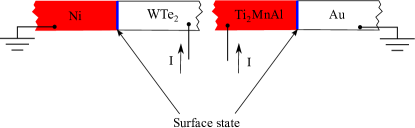
We prepare two types of interface structures. One of them is the junction between a gold normal layer and a magnetic Weyl semimetal Ti2MnAl, see Fig. 1 (b). The other one is the junction niwte between a ferromagnetic nickel layer and a non-magnetic Weyl semimetal WTe2. In both cases, 50 nm thick metallic film (nickel or gold) is thermally evaporated on the insulating SiO2 substrate. For nickel evaporation, the substrate is mounted on the in-plane magnetized sample holder. 10 m wide metallic leads are formed by photolithography and lift-off technique. Small (about 100 m size and 1 m thick) WTe2 flakes can be easily obtained from layered WTe2 single crystals. For Ti2MnAl, flakes are obtained by a mechanical cleaving method, see Fig. 1 (a). Then we select the most plane-parallel Ti2MnAl flakes with clean surface, where no surface defects could be resolved with optical microscope. A single flake (WTe2 or Ti2MnAl) is transferred on top of the metallic leads with overlap and pressed slightly with another oxidized silicon substrate. A special metallic frame allows us to keep the substrates parallel and apply a weak pressure to the sample. No external pressure is needed for a flake to hold on to a substrate with metallic leads afterward. This procedure provides transparent Ni-WTe2 or Au-Ti2MnAl junctions, stable in different cooling cycles, which has been also demonstrated before cdas ; nbwte ; niwte .
We investigate transport properties of a single Ni-WTe2 or Au-Ti2MnAl junction by a three-point technique, see Fig. 1 (b): a studied contact is grounded, two other contacts are employed to apply current and measure voltage , respectively. To obtain characteristics, the dc current is additionally modulated by a low ac component (2 A, kHz). We measure both dc () and ac (which is proportional to ) components of the voltage drop with a dc voltmeter and a lock-in, respectively. Measured ac signal is independent of frequency in 1-5 kHz range, which is defined by applied ac filters. In the connection scheme in Fig. 1 (b), all the wire resistances are excluded, which is necessary for low-impedance samples. The measurements are performed in a dilution refrigerator for the temperature interval 30 mK–1.2 K for two different orientations of the magnetic field to the interface. To ensure the homogeneous magnetic state of the junctions, the magnetization procedure is performed: an external magnetic field is swept slowly from zero to 5 T, afterward, the external field goes down to zero.
III Experimental results
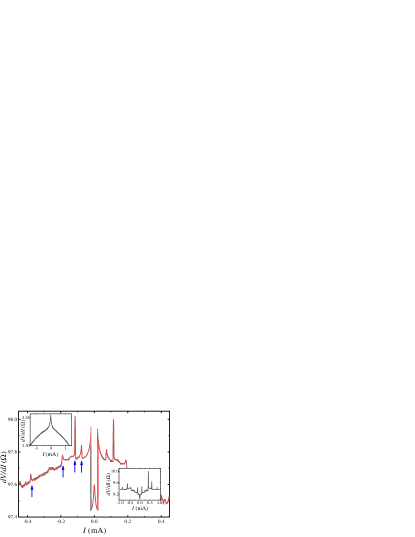
Fig. 2 provides typical examples of low-temperature characteristics for Au-Ti2MnAl (in the main field) and Ni-WTe2 (in the right inset) junctions. Despite different materials, we observe similar qualitative behavior for both types of the interfaces: curves are non-linear, there are peaks at high currents, and sharp symmetric switchings of differential resistance at low, A bias. The peaks’ positions are independent of the current sweep direction, while switchings at A demonstrates well-defined hysteresis.
We should connect the observed features with interface effects. In a three-point technique, the measured potential reflects in-series connected resistances of the Ni-WTe2 or Au-Ti2MnAl interface and some part of the crystal flake. From independence of the particular choice of current and voltage probes in Fig. 1 (b), we verify that the interface resistance dominates in the obtained curves. Also, we do not observe any features in bulk properties of Ti2MnAl, which is demonstrated by four-point measurements in the left inset to Fig. 2.
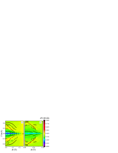
The obtained features can be suppressed by temperature or magnetic field above 1 K or 0.5 T, respectively, see Fig. 3. The positions of both the peaks and resistance switchings are moving to zero current with temperature increase until complete disappearance at 1.2 K, as depicted in Fig. 3 (a). Evolution of curves with magnetic field is different: the width of the low-current region (A) is nearly independent of the magnetic field, while the switching amplitude is gradually diminishing with the field. In contrast, peaks’ positions move to zero in a complicated manner.
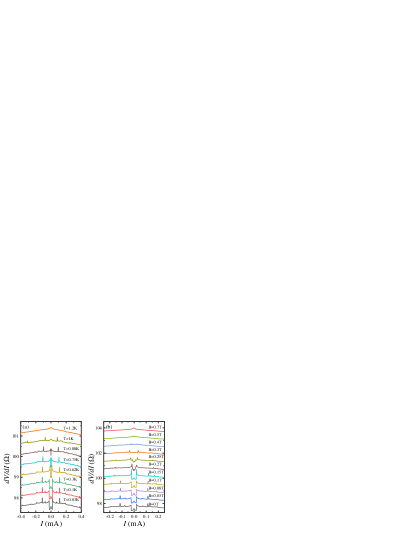
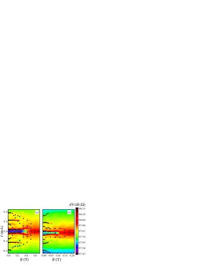
The detailed behavior of peaks’ positions is shown in Fig. 4 for Au-Ti2MnAl junction for parallel (a) and normal (b) to the interface magnetic fields. For both field orientations, the positions of the peaks are shifting non-monotonously to smaller currents, so the peaks disappears above some value of magnetic field. This value is significantly smaller for the normal field orientation ( T, see Fig. 4 (b)), in comparison with T for the parallel one (a).
IV Discussion
As a result, both Au-Ti2MnAl and Ni-WTe2 junctions demonstrate similar characteristics, with hysteresis at low currents and sharp peaks at high ones. Moreover, we observe qualitatively similar evolution of the peaks’ positions with magnetic field for both structures in Figs. 4 and 5. For this reason, the obtained results should have the same origin for these structures. From the experimental point of view, the obtained curves are similar to ones for ferromagnetic multilayers myers ; tsoi1 ; tsoi2 ; katine ; single ; balkashin ; balashov .
Weyl surface state is the only common characteristic armitage ; das16 ; feng2016 ; timnal of Au-Ti2MnAl and Ni-WTe2 interfaces, since the materials are completely different for the metallic contacts and the semimetals itself: for Au-Ti2MnAl junction we study transport between a magnetically-ordered WSM and a normal metal, while Ni-WTe2 one represents the junction between a non-magnetic WSM and a ferromagnet, see Fig. 6. Also, strong temperature dependence in the 30 mK-1.2 K range can only originate from the surface, since transport properties of Ni or Au layers and bulk WSM lvEPL15 ; timnal_exp are invariant in this temperature range.
For Au-Ti2MnAl and Ni-WTe2 samples, one side of the junction has significant net spin polarization of carriers (Ni or Ti2MnAl, respectively). We should conclude, that similar curves are produced by spin-polarized transport through the Weyl surface state at the interface. In some sense, our experiment resembles ones on ferromagnetic multilayers, where spin-dependent scattering affects the magnetic moments of the spin-polarized layers, while their mutual orientation defines the differential resistance myers ; tsoi1 ; tsoi2 ; katine ; single ; balkashin ; balashov . It might be natural topinssurf ; current , that we observe similar characteristics.
Let us start from switchings at low currents in Fig. 2. At zero bias, one can expect that spin polarization of some carriers at the WSM surface is aligned parallel to one in the ferromagnet due to the complicated spin texture texture ; araki on the Weyl surface jiang15 ; rhodes15 ; das16 ; feng2016 . For this reason, even spin-polarized carriers have a direct transport channel, which is reflected in low junction resistance at zero bias. While increasing the current through the junction, spin-momentum locking produces current ; araki a preferable spin polarization in the surface state, which is reflected as sharp increase for both signs of the current. As usual myers , current-induced switchings are accompanied by hysteresis in Fig. 2. Spin alignment disappears at zero bias, when high magnetic field or temperature destroys the spin textures in the topological surface state, see Fig. 3 (a) and (b).
Similarly to the ferromagnetic multilayers tsoi1 ; tsoi2 , we should identify peaks in Fig. 2 as the onset of the current-driven magnon excitations. However, evolution of the peaks’ positions with magnetic field is unusual: the peaks are moving to lower currents in Figs. 4 and 5, which is opposite to the known bulk magnon behavior myers ; tsoi1 ; tsoi2 ; katine ; single ; balkashin ; balashov ; cosns . This peaks’ evolution is the main difference of our results from the standard magnon experiments myers ; tsoi1 ; tsoi2 ; katine ; single ; balkashin ; balashov ; cosns .
Since the peaks disappear simultaneously with switchings in Fig. 3 (a) and (b), we should also connect topinssurf the magnon excitation with spin textures texture ; araki in the topological surface states. In general, the peak position is described by Slonczewski model slonczewski ; katine . Slightly simplified,
| (1) |
where is the damping parameter, is the gyromagnetic ratio, is the total spin of the free layer. In contrast to multilayers, the total spin is not a constant. It is diminishing to zero when high magnetic field or temperature destroys the spin textures in the topological surface state. This dependence can be the origin of the unusual peaks’ evolution in Figs. 3, 4 and 5. However, we have no complete description of the magnon dynamics in Weyl topological surface states, in contrast to the case of topological insulators topinssurf .
It is well known, that surface state transport can be observed only at temperatures, which are significantly lower than the temperature of the corresponding spectrum gap. For example, for the quantum Hall effect, temperatures below 1 K were necessary to see the edge state transport muller ; alida ; MZ . The same situation is for topological insulators amit ; kononov . For Weyl semimetals, we also observed nbwte Weyl specifics in Andreev reflection only below 1 K, while the Nb gap was estimated as about 10 K in this experiment. Strong temperature dependence in Fig. 3 (a) is in a contrast with known bulk behavior myers ; tsoi1 ; tsoi2 ; katine ; single ; balkashin ; balashov ; cosns , which can also indicate the surface state origin of the observed peaks.
V Conclusion
As a conclusion, we experimentally compare two types of interface structures with magnetic and non-magnetic Weyl semimetals. They are the junctions between a gold normal layer and magnetic Weyl semimetal Ti2MnAl, and a ferromagnetic nickel layer and non-magnetic Weyl semimetal WTe2, respectively. Due to the ferromagnetic side of the junction, we investigate spin-polarized transport through the Weyl semimetal surface. For both structures, we demonstrate similar current-voltage characteristics, with hysteresis at low currents and sharp peaks in differential resistance at high ones. Despite this behavior resembles the known current-induced magnetization dynamics in ferromagnetic structures, evolution of the resistance peaks with magnetic field is unusual. We connect the observed effects with current-induced spin dynamics in Weyl topological surface states.
Acknowledgements.
We wish to thank V.T. Dolgopolov for fruitful discussions, S.S Khasanov for X-ray sample characterization, A.A. Kononov and O.O. Shvetsov for help with experiment. We gratefully acknowledge financial support partially by the RFBR (project No. 19-02-00203), RAS, and RF State task.References
- (1) As a recent review see N.P. Armitage, E.J. Mele, and A. Vishwanath, Rev. Mod. Phys. 90, 015001 (2018).
- (2) P.K. Das, D.D. Sante, I. Vobornik, J. Fujii, T. Okuda, E. Bruyer, A. Gyenis, B.E. Feldman, J. Tao, R. Ciancio, G. Rossi, M.N. Ali, S. Picozzi, A. Yadzani, G. Panaccione, and R.J. Cava, Nature Comm. 7, 10847 (2016).
- (3) B. Feng, Y.-H. Chan, Y. Feng, R.-Y. Liu,1 M.-Y. Chou, K. Kuroda, K. Yaji, A. Harasawa, P. Moras, A. Barinov, W. Malaeb, C. Bareille, T. Kondo, S. Shin, F. Komori, T.-C. Chiang, Y. Shi, and I. Matsuda, Phys Rev B 94, 195134 (2016).
- (4) P. Li, Y. Wen, X. He1, Q. Zhang, C. Xia, Z.-M. Yu, S.A. Yang, Z. Zhu, H.N. Alshareef, X.-X. Zhang, Nature Comm. 8, 2150 (2017)
- (5) A.A. Soluyanov, D. Gresch, Z. Wang, Q. Wu, M. Troyer, X. Dai, B.A. Bernevig, Nature 527, 495 (2015).
- (6) X. Wan, A. M. Turner, A. Vishwanath, S. Y. Savrasov, Phys. Rev. B 83, 205101 (2011).
- (7) M. Hirschberger, S. Kushwaha, Z. Wang, Q. Gibson, S. Liang, C. A. Belvin, B. A. Bernevig, R. J. Cava, N. P. Ong, Nat. Mater. 15, 1161-1165 (2016).
- (8) G. Xu, H. Weng, Z. Wang, X. Dai, Z. Fang, Phys. Rev. Lett. 107, 186806 (2011).
- (9) S. K. Kushwaha, Z. Wang, T. Kong, R. J. Cava, J. Phys. Condens. Matter. 30, 075701 (2018).
- (10) Enke Liu, Yan Sun, Nitesh Kumar, Lukas Muechler, Aili Sun, Lin Jiao, Shuo-Ying Yang, Defa Liu, Aiji Liang, Qiunan Xu, Johannes Kroder, Vicky Süss, Horst Borrmann, Chandra Shekhar, Zhaosheng Wang, Chuanying Xi, Wenhong Wang, Walter Schnelle, Steffen Wirth, Yulin Chen, Sebastian T. B. Goennenwein, and Claudia Felser, Nature Physics 14, 1125 (2018)
- (11) Qi Wang, Yuanfeng Xu, Rui Lou, Zhonghao Liu, Man Li, Yaobo Huang, Dawei Shen, Hongming Weng, Shancai Wang and Hechang Lei, Nature Communications 9, 3681 (2018)
- (12) Wujun Shi, Lukas Muechler, Kaustuv Manna, Yang Zhang, Klaus Koepernik, Roberto Car, Jeroen van den Brink, Claudia Felser, and Yan Sun Phys. Rev. B 97, 060406(R).
- (13) Lukas Wollmann, Ajaya K. Nayak, Stuart S.P. Parkin, and Claudia Felser, Annual Review of Materials Research, 47, 247 (2017)
- (14) Wuwei Feng, Xiao Fu, Caihua Wan, Zhonghui Yuan, Xiufeng Han, Nguyen Van Quang, and Sunglae Cho, Phys. Status Solidi RRL 9, No. 11, 641–645 (2015); DOI 10.1002/pssr.201510340
- (15) E.B. Myers, D.C. Ralph, J.A. Katine, R.N. Louie, R.A. Buhrman, Science, 285, 867 (1999).
- (16) M. Tsoi, A. G. M. Jansen, J. Bass, W.-C. Chiang, M. Seck, V. Tsoi, and P. Wyder, Phys. Rev. Lett., 80, 4281 (1998).
- (17) M. Tsoi, A. G. M. Jansen, J. Bass, W.-C. Chiang, V. Tsoi and P. Wyder, Nature, 406, 46, (2000).
- (18) J. A. Katine, F. J. Albert, R. A. Buhrman, E. B. Myers and D. C. Ralph, Phys. Rev. Lett., 84, 3149 (2000)
- (19) Y. Ji, C. L. Chien, and M. D. Stiles, Phys. Rev. Lett., 90, 106601 (2003)
- (20) O. P. Balkashin, V. V. Fisun, I. K. Yanson, L. Yu. Triputen, A. Konovalenko, and V. Korenivski, Phys. Rev. B, 79, 092419 (2009)
- (21) T. Balashov, A. F. Takács, M. Däne, A. Ernst, P. Bruno, and W. Wulfhekel, Phys. Rev. B, 78, 174404 (2008)
- (22) O. O. Shvetsov, V. D. Esin, A. V. Timonina, N. N. Kolesnikov, E. V. Deviatov, EPL, 127, 57002 (2019), doi: 10.1209/0295-5075/127/57002
- (23) Jimmy A. Hutasoit, Jiadong Zang, Radu Roiban, and Chao-Xing Liu, Phys. Rev. B 90, 134409 (2014)
- (24) Steven S.-L. Zhang, Anton A. Burkov, Ivar Martin, Olle G. Heinonen, Phys. Rev. Lett. 123, 187201 (2019); DOI: 10.1103/PhysRevLett.123.187201
- (25) J. Jiang, F. Tang, X.C. Pan, H.M. Liu, X.H. Niu, Y.X. Wang, D.F. Xu, H.F. Yang, B.P. Xie, F.Q. Song, P. Dudin, T.K. Kim, M. Hoesch, P.K. Das, I. Vobornik, X.G. Wan, and D.L. Feng, Phys. Rev. Lett. 115, 166601 (2015).
- (26) D. Rhodes, S. Das, Q.R. Zhang, B. Zeng, N.R. Pradhan, N. Kikugawa, E. Manousakis, and L. Balicas, Phys. Rev. B 92, 125152 (2015).
- (27) Y.Wang, K.Wang, J. Reutt-Robey, J. Paglione, and M. S. Fuhrer, Phys. Rev. B 93, 121108 (2016).
- (28) Daichi Kurebayashi, Naoto Nagaosa, Phys. Rev. B 100, 134407 (2019); DOI: 10.1103/PhysRevB.100.134407
- (29) P. O. Sukhachov, M. V. Rakov, O. M. Teslyk, E. V. Gorbar, arXiv:1909.10587
- (30) Yasufumi Araki, Ann. Phys. (Berlin) 1900287 (2019), DOI: 10.1002/andp.201900287
- (31) Y. Araki and K. Nomura, Phys. Rev. B 93, 094438 (2016)
- (32) E. B. Borisenko, V. A. Berezin, N. N. Kolesnikov, V. K. Gartman, D. V. Matveev, O. F. Shakhlevich, Physics of the Solid State, 59, 1310, (2017).
- (33) A. Sidorov, A.E. Petrova, A.N. Pinyagin, N.N. Kolesnikov, S.S. Khasanov, S.M. Stishov, JETP, 122, 1047, (2016).
- (34) M.N. Ali, J. Xiong, S. Flynn, J. Tao, Q.D. Gibson, L.M. Schoop, T. Liang, N. Haldolaarachchige, M. Hirschberger, N.P. Ong, and R.J. Cava, Nature (London) 514, 205 (2014).
- (35) H.Y. Lv, W.J. Lu, D.F. Shao, Y. Liu, S.G. Tan, and Y.P. Sun, Europhys. Lett. 110, 37004 (2015).
- (36) O. O. Shvetsov, V. D. Esin, A. V. Timonina, N. N. Kolesnikov, and E. V. Deviatov Phys. Rev. B 99, 125305 (2019)
- (37) A. Kononov, O.O. Shvetsov, S.V. Egorov, A.V. Timonina, N.N. Kolesnikov and E.V. Deviatov EPL, 122, 27004 (2018)
- (38) A. Kononov, O. O. Shvetsov, A. V. Timonina, N. N. Kolesnikov, E. V. Deviatov, JETP Letters, 109, 180 (2019). DOI: 10.1134/S0021364019030020
- (39) J.C. Slonczewski, J. Magn. Magn. Mater., 159, L1, (1996).
- (40) G. Müller, D. Weiss, A. V. Khaetskii, K. von Klitzing, S. Koch, H. Nickel, W. Schlapp, and R. Lösch, Phys. Rev. B 45, 3932(R) (1992)
- (41) A. Würtz, R. Wildfeuer, A. Lorke, E. V. Deviatov, and V. T. Dolgopolov, Phys. Rev. B 65, 075303 (2002)
- (42) E.V. Deviatov, A. Ganczarczyk, A. Lorke, G. Biasiol, and L. Sorba, Phys. Rev. B 84, 235313 (2011)
- (43) Amit Jash, Kamalika Nath, T.R. Devidas, A. Bharathi, and S.S. Banerjee, Phys. Rev. Applied 12, 014056 (2019)
- (44) A. Kononov, V. A. Kostarev, B. R. Semyagin, V. V. Preobrazhenskii, M. A. Putyato, E. A. Emelyanov, and E. V. Deviatov, Phys. Rev. B 96, 245304 (2017)