A laser-ARPES study of LaNiO3 thin films grown by sputter deposition
Abstract
Thin films of the correlated transition-metal oxide LaNiO3 undergo a metal-insulator transition when their thickness is reduced to a few unit cells. Here, we use angle-resolved photoemission spectroscopy to study the evolution of the electronic structure across this transition in a series of epitaxial LaNiO3 films of thicknesses ranging from 19 to 2 u.c. grown in situ by RF magnetron sputtering. Our data show a strong reduction of the electronic mean free path as the thickness is reduced below 5 u.c. This prevents the system from becoming electronically two-dimensional, as confirmed by the largely unchanged Fermi surface seen in our experiments. In the insulating state we observe a strong suppression of the coherent quasiparticle peak but no clear gap. These features resemble previous observations of the insulating state of NdNiO3.
The members of the rare-earth nickelate series NiO3 ( = La, Pr, Nd…) undergo a first-order metal-insulator transition (MIT) from a high-temperature correlated metallic phase to a paramagnetic insulating phase followed by a transition to an antiferromagnetic ground state. The critical temperature of both transitions varies with the rare-earth element and correlates with the increasing distortion of the NiONi bond angle with decreasing rare-earth ionic radius Medarde (1997); Catalano et al. (2018). The MIT is accompanied by a breathing distortion in which two inequivalent Ni sites with different NiO bond lengths are arranged in a three-dimensional (3D) checkerboard pattern. The resulting bond disproportionation leads to electron localization on one of the sublattices and can thus be seen as a site-selective Mott transition, which is strongly coupled to the lattice, while magnetic order seems to play a secondary role Park, Millis, and Marianetti (2012); Peil et al. (2019).
LaNiO3 (LNO) represents an exception in the NiO3 family in that it remains metallic all the way down to the lowest temperatures. The metallic phase is on the brink of a MIT, and its low-temperature magnetic state is still under debate Sánchez et al. (1993); Guo et al. (2018). Experiments on thin films have shown that it is possible to modulate the transport properties by electric-field gating Scherwitzl et al. (2009) and by tuning the strain on the lattice Son et al. (2010); Chakhalian et al. (2011). Moreover, a transition to an insulating state at all temperatures has been achieved by inducing oxygen vacancies Sánchez et al. (1996) or by reducing the thickness of the material down to a few unit cells (u.c.) Scherwitzl et al. (2011); Sakai et al. (2013); King et al. (2014); Golalikhani et al. (2018). This latter thickness-dependent transition was originally ascribed to strong localization, based on evidence from transport experiments for a mean free path below the Ioffe-Regel limit , where is the Fermi wave vector and the mean free path Scherwitzl et al. (2011). It was later pointed out that structural distortions at the surface of LNO thin films, which have been observed both in scanning transmission electron microscopy (STEM) and X-ray diffraction experiments, could also play a role. In fact, both the top LNO-vacuum and the bottom LNO-substrate interfaces of thin films have been shown to be characterized by different conductivity and structural properties with respect to the interior Chen et al. (2013); Kumah et al. (2014); Fowlie et al. (2017); Ruf et al. (2017). Most strikingly, Kumah et al. Kumah et al. (2014) were able to turn an insulating film metallic by adding a LaAlO3 (LAO) capping layer, which suppressed the surface relaxation. This experiment demonstrated the key role of such relaxations and evidenced the fact that confined LNO layers in superlattices behave differently than the films with a free surface that we study here Kumah et al. (2014); Golalikhani et al. (2018). There is still no consensus regarding the nature of the insulating state in thin films, and the question of whether it is possible to stabilize a metallic 1-u.c.-thick LNO film remains open.
Over the past decade, several angle-resolved photoemission (ARPES) studies have been conducted on LNO epitaxial films grown by pulsed-laser deposition (PLD) and molecular-beam epitaxy (MBE). The Fermi surface of the correlated metallic phase has been found to be in good qualitative agreement with density functional theory (DFT) predictions for thick films, yet the reports are conflicting for thinner films Eguchi et al. (2009); King et al. (2014); Yoo et al. (2016). King et al. King et al. (2014) reported a 3D electronic structure as well as a MIT characterized by a loss of coherent quasiparticles at and a thickness-independent electronic mean free path, while Yoo et al. Yoo et al. (2016) observed a modified Fermi surface for films thinner than 4 u.c., with signatures of a quasi-1D electronic structure. The former study attributed the onset of the insulating state to a fluctuating spin order enhanced by dimensionality, while the latter argued for the importance of 1D-Fermi-surface nesting in determining the MIT; a clear answer remains to be found. Some features of the spectral function of insulating LNO thin films are shared by thick insulating NdNiO3 (NNO) films. Indeed, Dhaka et al. Dhaka et al. (2015) reported a drastic reduction of spectral weight at in NNO at temperatures just below the metal-insulator transition, so the possibility of a common origin for the insulating states in LNO and NNO thin films is open.
In this work, we report high-resolution laser-based ARPES measurements on a series of high-quality LNO films grown by sputter deposition. We show that the transition to increasingly insulating behavior with reduced thickness proceeds via a strong reduction in the quasiparticle mean free path and coherent weight, rather than the opening of a gap or a transition to electronically 2D behavior. We find that the spectral properties of the thinnest insulating samples are reminiscent of the low-temperature insulating state of NNO, suggesting a key role of structural relaxation at the surface.
A series of LNO films with thicknesses ranging from 2 to 19 u.c. (i.e. 7.5 to 71.8 Å) were grown on LAO (001) substrates by off-axis RF magnetron sputtering at a temperature C and pressure mbar in a mixed 7:2 Ar:O2 atmosphere. In order to limit the formation of oxygen vacancies, the films were left to cool down in a pure oxygen atmosphere, maintaining the growth pressure.
Immediately after growth, each film was transferred in vacuo to the laser-ARPES setup so as to reduce surface contamination, which can affect the quality of the photoemission spectra. Photoemission experiments were performed with an electron spectrometer from MB Scientific and a narrow-bandwidth 11-eV pulsed laser from Lumeras, operated at a repetition rate of 50 MHz with 30 ps pulses of the fundamental infrared wavelength. The energy resolution was meV, which was verified by fitting the Fermi edge of a polycrystalline gold sample, while the angular resolution was Å-1. These values are well below the line widths observed in our experiments. The samples were mounted on a cryogenic 6-axes goniometer Hoesch et al. (2017) and measured at a temperature of K with the exception of the 2-u.c. film, which was measured at K in order to limit sample charging due to its insulating nature.
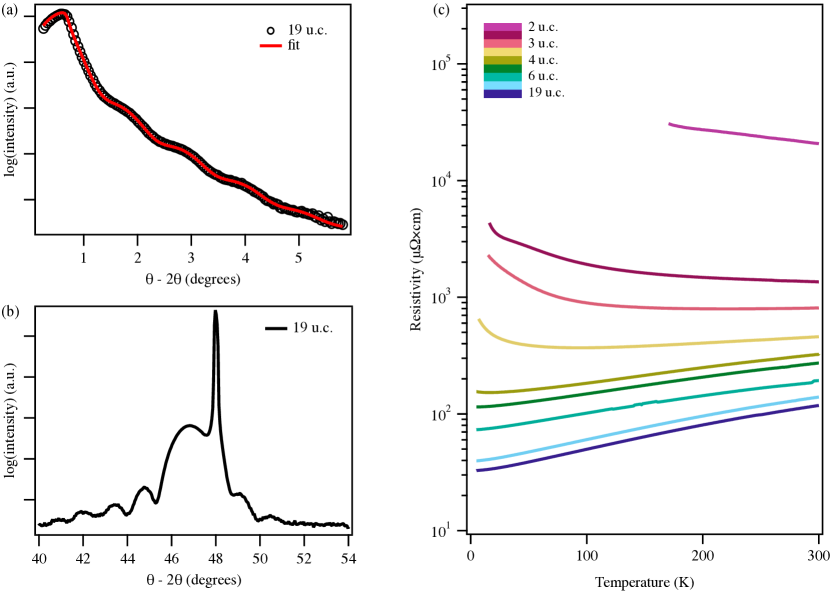
The structural quality of the samples was characterized by x-ray reflectivity (XRR) and diffraction (XRD) scans using a Philips X’Pert 1 diffractometer equipped with a Cu K source ( Å). Figures 1(a) and (b) show XRR and XRD plots respectively for a 19-u.c.-thick sample. The reflectivity data was fitted using GenX in order to obtain the film thickness used to calibrate the growth rate and the surface roughness, which is below 1 u.c. for all films Björck and Andersson (2007). The XRD measurements show a sharp Bragg peak, corresponding to the LAO (002) planes, as well as a broader peak with side oscillations from the LNO thin film. The thickness obtained from these oscillations is consistent with the value extracted from the XRR fit. All in all, the quality of the XRD data and films is consistent with previous studies Fowlie et al. (2017).
Platinum electrical contacts were deposited at the four corners of the samples. The sheet resistance was measured over a temperature range of 5 to 300 K in a Quantum Design Physical Property Measurement System using the standard van der Pauw configuration Van der Pauw (1958). Figure 1(c) shows resistivity curves as a function of temperature for all the LNO films. The residual resistivity ratios (RRR) for the metallic films (419 u.c.) vary between 3.5 and 2 and are comparable to the values measured for films grown by sputter deposition Scherwitzl et al. (2009, 2011); Fowlie et al. (2017) and pulsed-laser deposition (PLD) Horiba et al. (2007); Golalikhani et al. (2018), but 2-3 times lower than the RRR of the MBE-grown films measured in Ref. King et al. (2014). We can observe 3 different transport regimes: films thicker than 5 u.c. are metallic () all the way from room temperature down to the base temperature of K. The resistivity of thinner films presents an upturn at low temperatures that has been observed before Scherwitzl et al. (2011); King et al. (2014); Wang et al. (2019) and was attributed to weak localization effects Son et al. (2010); Scherwitzl et al. (2011). Finally, films thinner than 3 u.c. are insulating up to room temperature. These findings are fully consistent with previous reports for LNO films grown on LAO King et al. (2014); Fowlie et al. (2017); Golalikhani et al. (2018).
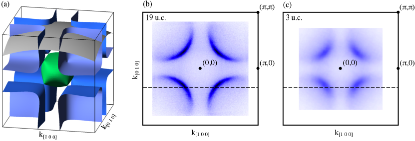
Figure 2(a) shows a tight-binding calculation of the three-dimensional Fermi surface of bulk LNO, which was performed using the parameters introduced by Lee et al. Lee, Chen, and Balents (2011) and refined to fit ARPES measurements by Bruno et al. Bruno et al. (2017). The Fermi surface originates mainly from Ni orbitals and is composed of a nearly spherical electron pocket centred at and hole pockets at the Brillouin-zone corners. Figure 2(b) displays the photoemission intensity at the Fermi level obtained for the 19-u.c.-thick sample. We find well-defined nearly circular Fermi-surface contours centered at the Brillouin-zone corners. These contours have an arc-like appearance with a weight that rapidly decays away from the zone diagonal, reminiscent of underdoped cuprates Shen et al. (2005). However, a careful inspection of the data does not show any signs of a momentum-dependent quasiparticle linewidth or of the opening of a pseudogap. We thus attribute the weight distribution to momentum-dependent matrix elements.
The photon energy of 11 eV used in our experiments probes the electronic structure along a spherical contour, as depicted in gray in Figure 2(a). As long as the electronic structure remains 3D, our measurements thus capture the large hole pockets, while no signal is expected from the electron pocket at the zone center, in agreement with the data in 2(b). This would no longer be the case if the electronic structure were to become 2D and therefore lose all dependence, as reported in Ref. Yoo et al. (2016). In this case, our measurements should pick up a signal from the electron pocket at , which is predicted to remain occupied down to a thickness of 2 u.c. Fowlie et al. (2017) The largely unchanged Fermi-surface contour for a film with a thickness of 3 u.c., as shown in Figure 2(c), and the absence of the zone-center electron pocket in this measurement indicate that a transition to 2D behavior does not occur even in ultrathin films. This discrepancy might be related to the improved resolution of the present study or to factors related to the films themselves, such as surface and interface roughness and film cleanliness, which we expect to influence the effective dimensionality of the electronic structure. We clarify that the electronic dimensionality is different from, albeit related to, the reduced geometric dimensionality dictated by the thinness of the film.
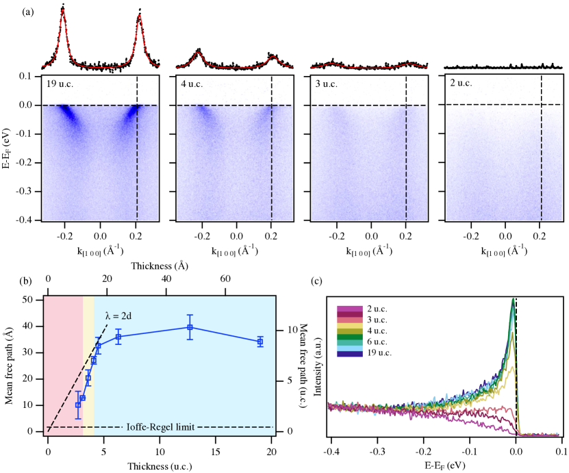
Figure 3(a) shows the electronic band dispersion measured along the dashed line in Figure 2(b). In these measurements, corresponding to films of thickness 19, 4, 3 and 2 u.c., we observe the evolution of the bands which form the hole-like pockets centred at the Brillouin-zone corners. The suppression of intensity near can be attributed to matrix elements and is consistent with an approximately parabolic band closing at , as expected theoretically and reported in previous experiments King et al. (2014). By examining these cuts, it is evident that the spectral weight at the Fermi edge is progressively lost as the film thickness is reduced and the material turns insulating. On the other hand, the overall band dispersion and the Fermi wave vector remain largely unchanged down to a thickness of 3 u.c., which shows weakly insulating behavior at all temperatures in transport.
Next, we evaluate the mean free path of the charge carriers as a function of film thickness. The mean free path measured by ARPES is defined as , where is the full width at half maximum (FWHM) of the peak in a momentum distribution curve (MDC) taken normal to the Fermi surface. To determine we thus fit the MDCs displayed in Figure 3(a) by Lorentzians (shown in red) and correct their FWHM by a geometric factor accounting for the angle of between the measured -space cut and the Fermi surface contour.
The values of extracted by following this procedure are presented in Figure 3(b). The red, yellow, and blue shaded areas correspond to the 3 transport regimes discussed previously. We find that the mean free path follows two distinct regimes. For films up to 5 u.c. thickness, increases almost linearly from Å to Å. In thicker films, rapidly saturates at values below Å. We first note that these values exceed the thickness-independent value of 8 Å reported in earlier ARPES experiments King et al. (2014). We attribute this predominantly to the improved experimental conditions resulting from a higher spectrometer resolution, the smaller light spot size, which limits the inhomogeneous broadening arising from the average over a large surface area, and the lower photon energy, which reduces the broadening induced by the intrinsically poor resolution of ARPES . On the other hand, the values of obtained here remain below the 100 Å deduced from magneto-transport experiments Scherwitzl et al. (2011). We can presently not exclude that this is due to limitations in the effective resolution of our ARPES experiments which are notoriously hard to quantify. However, this might also be of fundamental origin. The mean free path measured by ARPES contains all scattering events out of a particular -state, while transport is predominantly sensitive to large-angle scattering. ARPES thus generally measures a lower limit of the transport mean free path. Secondly, we note that the evolution of naturally explains the puzzling absence of quantum-well states reported in all previous ARPES experiments on ultrathin LNO films, even though they appear in band structure calculations where they show a subband splitting that should be readily resolved in experiment King et al. (2014); Yoo et al. (2016); Fowlie et al. (2017). Quantum-well states — and thus a genuinely 2D electronic structure — can only exist if the coherence length of the electronic states significantly exceeds the film thickness. As shown in Figure 3(b), this is not the case in our films. The sharp reduction for the thinnest films limits the coherence length to below twice the film thickness (indicated by a dashed line in Figure 3(b)), which prohibits the coherent superposition of wave packets reflected at the surface and interface and thus the formation of quantum-well states. We finally note that the transition from a nearly constant to a sharply decreasing mean free path at a thickness of 5 u.c. coincides with the onset of an upturn in resistivity. This points to a complex interplay of interactions and disorder, rather than to weak localization as the main origin of the resistivity upturn Alloul et al. (2009). Our ARPES data also show that the mean free path remains well above the Ioffe-Regel limit of even for the 3 u.c. film, which is insulating in transport, suggesting that the thickness-dependent MIT is not induced by strong localization Gunnarsson, Calandra, and Han (2003); Scherwitzl et al. (2011); Wang et al. (2019).
We now turn our attention to the origin of the sharp reduction in mean free path as the thickness is reduced below 5 u.c. At first sight, the nearly linear dependence of the mean free path on film thickness appears to suggest a dominant contribution of elastic defect scattering at the interface and surface. However, while interface roughness and the presence of defects such as oxygen vacancies will inevitably contribute to limiting the mean free path, it cannot readily explain the abrupt change in the thickness dependence of at 5 u.c. The latter rather points to an important role of fluctuations near the MIT. It has previously been suggested that such fluctuations might be enhanced by the reduced dimensionality of ultrathin films Boris et al. (2011); King et al. (2014). A reduced dimensionality is, however, not confirmed by our data, which show that films down to 3 u.c. do not become electronically 2D. In contrast to Ref King et al. (2014), we believe that fluctuations might also be enhanced by the inevitable structural relaxation of 3D perovskites at interfaces and surfaces. It is known that such relaxations are particularly strong in nickelates and move the outermost unit cells of LNO closer to an insulating state Kumah et al. (2014), which shares similarities with the ground state of other rare-earth nickelates. In the vicinity of such an insulating state with putative antiferromagnetic order, bond and charge disproportionation, as well as fluctuations of spin, lattice, and charge degrees of freedom should be strong and can have a decisive effect on quasiparticle coherence. This interpretation is further supported by the overall similarity of the spectral function in ultrathin LNO films with earlier observations of NNO films below the MIT Dhaka et al. (2015). It is, however, at odds with the absence of bond disproportionation and metallic state reported by DFT calculations for a 2-u.c.-thick film in Ref Fowlie et al. (2017). Most imporantly, both systems show a gradual suppression of spectral weight near the Fermi level, rather than a clear gap both in optical and photoemission measurements Dhaka et al. (2015); Ruppen et al. (2015). We thus speculate that the MIT in ultrathin LNO is neither driven primarily by the reduced dimensionality, nor by defects, but rather by structural relaxation of the ultra-thin films.
In conclusion, we demonstrated that the combination of sputter deposition and laser ARPES provides high-quality data showing significantly narrower quasiparticle line widths than obtained previously. This establishes sputter deposition as an attractive alternative to MBE or PLD growth for in-situ electronic structure studies. Our data revealed a strong dependence of the quasiparticle mean free path on sample thickness, which was previously unresolved and can explain the universally reported absence of quantum-well states in ARPES experiments on nickelate thin films. The similarity between the electronic structures of 2-3-u.c.-thick LNO films and insulating NNO further points to an important role of structural relaxation at the interface or surface in the MIT of ultrathin LNO films.
Acknowledgements.
This work has been supported by the Swiss National Science Foundation (Ambizione Grant No. PZ00P2-161327 and project grants 165791, 184998) and by Comunidad de Madrid (Atraccion de Talento grant No. 2018-T1/IND-10521).References
- Medarde (1997) M. L. Medarde, “Structural, magnetic and electronic properties of perovskites (R = rare earth),” Journal of Physics: Condensed Matter 9, 1679–1707 (1997).
- Catalano et al. (2018) S. Catalano, M. Gibert, J. Fowlie, J. Íñiguez, J.-M. Triscone, and J. Kreisel, “Rare-earth nickelates RNiO3: thin films and heterostructures,” Reports on Progress in Physics 81, 046501 (2018).
- Park, Millis, and Marianetti (2012) H. Park, A. J. Millis, and C. A. Marianetti, “Site-selective mott transition in rare-earth-element nickelates,” Phys. Rev. Lett. 109, 156402 (2012).
- Peil et al. (2019) O. E. Peil, A. Hampel, C. Ederer, and A. Georges, “Mechanism and control parameters of the coupled structural and metal-insulator transition in nickelates,” Phys. Rev. B 99, 245127 (2019).
- Sánchez et al. (1993) R. Sánchez, M. Causa, J. Sereni, M. Vallet-Regí, M. Sayagués, and J. González-Calbet, “Specific heat, magnetic susceptibility and electrical resistivity measurements on LaNiO3,” Journal of Alloys and Compounds 191, 287 – 289 (1993).
- Guo et al. (2018) H. Guo, Z. W. Li, L. Zhao, Z. Hu, C. F. Chang, C. Y. Kuo, W. Schmidt, A. Piovano, T. W. Pi, O. Sobolev, D. I. Khomskii, L. H. Tjeng, and A. C. Komarek, “Antiferromagnetic correlations in the metallic strongly correlated transition metal oxide LaNiO3,” Nature Communications 9, 43 (2018).
- Scherwitzl et al. (2009) R. Scherwitzl, P. Zubko, C. Lichtensteiger, and J.-M. Triscone, “Electric-field tuning of the metal-insulator transition in ultrathin films of LaNiO3,” Applied Physics Letters 95, 222114 (2009).
- Son et al. (2010) J. Son, P. Moetakef, J. M. LeBeau, D. Ouellette, L. Balents, S. J. Allen, and S. Stemmer, “Low-dimensional mott material: Transport in ultrathin epitaxial LaNiO3 films,” Applied Physics Letters 96, 062114 (2010).
- Chakhalian et al. (2011) J. Chakhalian, J. M. Rondinelli, J. Liu, B. A. Gray, M. Kareev, E. J. Moon, N. Prasai, J. L. Cohn, M. Varela, I. C. Tung, M. J. Bedzyk, S. G. Altendorf, F. Strigari, B. Dabrowski, L. H. Tjeng, P. J. Ryan, and J. W. Freeland, “Asymmetric orbital-lattice interactions in ultrathin correlated oxide films,” Phys. Rev. Lett. 107, 116805 (2011).
- Sánchez et al. (1996) R. D. Sánchez, M. T. Causa, A. Caneiro, A. Butera, M. Vallet-Regí, M. J. Sayagués, J. González-Calbet, F. García-Sanz, and J. Rivas, “Metal-insulator transition in oxygen-deficient LaNiO3-x perovskites,” Phys. Rev. B 54, 16574–16578 (1996).
- Scherwitzl et al. (2011) R. Scherwitzl, S. Gariglio, M. Gabay, P. Zubko, M. Gibert, and J.-M. Triscone, “Metal-insulator transition in ultrathin LaNiO3 films,” Phys. Rev. Lett. 106, 246403 (2011).
- Sakai et al. (2013) E. Sakai, M. Tamamitsu, K. Yoshimatsu, S. Okamoto, K. Horiba, M. Oshima, and H. Kumigashira, “Gradual localization of Ni states in LaNiO3 ultrathin films induced by dimensional crossover,” Phys. Rev. B 87, 075132 (2013).
- King et al. (2014) P. D. C. King, H. I. Wei, Y. F. Nie, M. Uchida, C. Adamo, S. Zhu, X. He, I. Božović, D. G. Schlom, and K. M. Shen, “Atomic-scale control of competing electronic phases in ultrathin LaNiO3,” Nature Nanotechnology 9, 443 (2014).
- Golalikhani et al. (2018) M. Golalikhani, Q. Lei, R. U. Chandrasena, L. Kasaei, H. Park, J. Bai, P. Orgiani, J. Ciston, G. E. Sterbinsky, D. A. Arena, P. Shafer, E. Arenholz, B. A. Davidson, A. J. Millis, A. X. Gray, and X. X. Xi, “Nature of the metal-insulator transition in few-unit-cell-thick LaNiO3 films,” Nature Communications 9, 2206 (2018).
- Chen et al. (2013) H. Chen, D. P. Kumah, A. S. Disa, F. J. Walker, C. H. Ahn, and S. Ismail-Beigi, “Modifying the electronic orbitals of nickelate heterostructures via structural distortions,” Phys. Rev. Lett. 110, 186402 (2013).
- Kumah et al. (2014) D. P. Kumah, A. S. Disa, J. H. Ngai, H. Chen, A. Malashevich, J. W. Reiner, S. Ismail-Beigi, F. J. Walker, and C. H. Ahn, “Tuning the structure of nickelates to achieve two-dimensional electron conduction,” Advanced Materials 26, 1935–1940 (2014).
- Fowlie et al. (2017) J. Fowlie, M. Gibert, G. Tieri, A. Gloter, J. Íñiguez, A. Filippetti, S. Catalano, S. Gariglio, A. Schober, M. Guennou, J. Kreisel, O. Stéphan, and J.-M. Triscone, “Conductivity and local structure of LaNiO3 thin films,” Advanced Materials 29, 1605197 (2017).
- Ruf et al. (2017) J. P. Ruf, P. D. C. King, V. B. Nascimento, D. G. Schlom, and K. M. Shen, “Surface atomic structure of epitaxial LaNiO3 thin films studied by in situ LEED-I(V),” Physical Review B 95 (2017).
- Björck and Andersson (2007) M. Björck and G. Andersson, “GenX: an extensible X-ray reflectivity refinement program utilizing differential evolution,” Journal of Applied Crystallography 40, 1174–1178 (2007).
- Eguchi et al. (2009) R. Eguchi, A. Chainani, M. Taguchi, M. Matsunami, Y. Ishida, K. Horiba, Y. Senba, H. Ohashi, and S. Shin, “Fermi surfaces, electron-hole asymmetry, and correlation kink in a three-dimensional fermi liquid LaNiO3,” Phys. Rev. B 79, 115122 (2009).
- Yoo et al. (2016) H. K. Yoo, S. I. Hyun, Y. J. Chang, L. Moreschini, C. H. Sohn, H.-D. Kim, A. Bostwick, E. Rotenberg, J. H. Shim, and T. W. Noh, “Thickness-dependent electronic structure in ultrathin LaNiO3 films under tensile strain,” Phys. Rev. B 93, 035141 (2016).
- Dhaka et al. (2015) R. S. Dhaka, T. Das, N. C. Plumb, Z. Ristic, W. Kong, C. E. Matt, N. Xu, K. Dolui, E. Razzoli, M. Medarde, L. Patthey, M. Shi, M. Radović, and J. Mesot, “Tuning the metal-insulator transition in NdNiO3 heterostructures via fermi surface instability and spin fluctuations,” Phys. Rev. B 92, 035127 (2015).
- Lee, Chen, and Balents (2011) S. Lee, R. Chen, and L. Balents, “Metal-insulator transition in a two-band model for the perovskite nickelates,” Phys. Rev. B 84, 165119 (2011).
- Bruno et al. (2017) F. Y. Bruno, M. Gibert, S. McKeown Walker, O. E. Peil, A. de la Torre, S. Riccò, Z. Wang, S. Catalano, A. Tamai, F. Bisti, V. N. Strocov, J.-M. Triscone, and F. Baumberger, “Electronic structure of buried LaNiO3 layers in (111)-oriented LaNiO3/LaMnO3 superlattices probed by soft x-ray ARPES,” APL Materials 5, 016101 (2017).
- Hoesch et al. (2017) M. Hoesch, T. K. Kim, P. Dudin, H. Wang, S. Scott, P. Harris, S. Patel, M. Matthews, D. Hawkins, S. G. Alcock, T. Richter, J. J. Mudd, M. Basham, L. Pratt, P. Leicester, E. C. Longhi, A. Tamai, and F. Baumberger, “A facility for the analysis of the electronic structures of solids and their surfaces by synchrotron radiation photoelectron spectroscopy,” Review of Scientific Instruments 88, 013106 (2017).
- Van der Pauw (1958) L. Van der Pauw, “A method of measuring the resistivity and hall coefficient on lamellae of arbitrary shape.” Philips Technical Review 20, 220–224 (1958).
- Horiba et al. (2007) K. Horiba, R. Eguchi, M. Taguchi, A. Chainani, A. Kikkawa, Y. Senba, H. Ohashi, and S. Shin, “In situ photoemission study of LaNiO3 thin films grown by pulsed laser deposition,” Journal of Electron Spectroscopy and Related Phenomena 156-158, 107 – 110 (2007).
- Wang et al. (2019) C. Wang, C.-H. Chang, A. Huang, P.-C. Wang, P.-C. Wu, L. Yang, C. Xu, P. Pandey, M. Zeng, R. Böttger, H.-T. Jeng, Y.-J. Zeng, M. Helm, Y.-H. Chu, R. Ganesh, and S. Zhou, “Tunable disorder and localization in the rare-earth nickelates,” Phys. Rev. Materials 3, 053801 (2019).
- Shen et al. (2005) K. M. Shen, F. Ronning, D. H. Lu, F. Baumberger, N. J. C. Ingle, W. S. Lee, W. Meevasana, Y. Kohsaka, M. Azuma, M. Takano, H. Takagi, and Z.-X. Shen, “Nodal quasiparticles and antinodal charge ordering in Ca2-xNaxCuO2Cl2,” Science 307, 901–904 (2005).
- Peil, Ferrero, and Georges (2014) O. E. Peil, M. Ferrero, and A. Georges, “Orbital polarization in strained LaNiO3: Structural distortions and correlation effects,” Physical Review B 90, 045128 (2014).
- Moser (2017) S. Moser, “An experimentalist’s guide to the matrix element in angle resolved photoemission,” Journal of Electron Spectroscopy and Related Phenomena 214, 29–52 (2017).
- Alloul et al. (2009) H. Alloul, J. Bobroff, M. Gabay, and P. J. Hirschfeld, “Defects in correlated metals and superconductors,” Rev. Mod. Phys. 81, 45–108 (2009).
- Gunnarsson, Calandra, and Han (2003) O. Gunnarsson, M. Calandra, and J. E. Han, “Colloquium: Saturation of electrical resistivity,” Rev. Mod. Phys. 75, 1085–1099 (2003).
- Boris et al. (2011) A. V. Boris, Y. Matiks, E. Benckiser, A. Frano, P. Popovich, V. Hinkov, P. Wochner, M. Castro-Colin, E. Detemple, V. K. Malik, C. Bernhard, T. Prokscha, A. Suter, Z. Salman, E. Morenzoni, G. Cristiani, H.-U. Habermeier, and B. Keimer, “Dimensionality control of electronic phase transitions in nickel-oxide superlattices,” Science 332, 937–940 (2011).
- Ruppen et al. (2015) J. Ruppen, J. Teyssier, O. E. Peil, S. Catalano, M. Gibert, J. Mravlje, J.-M. Triscone, A. Georges, and D. van der Marel, “Optical spectroscopy and the nature of the insulating state of rare-earth nickelates,” Phys. Rev. B 92, 155145 (2015).