Strong and Weak Three-Dimensional Topological Insulators Probed by Surface Science Methods
We review the contributions of surface science methods to discover and improve 3D topological insulator materials, while illustrating with examples from our own work. In particular, we demonstrate that spin-polarized angular-resolved photoelectron spectroscopy is instrumental to evidence the spin-helical surface Dirac cone, to tune its Dirac point energy towards the Fermi level, and to discover novel types of topological insulators such as dual ones or switchable ones in phase change materials. Moreover, we introduce procedures to spatially map potential fluctuations by scanning tunneling spectroscopy and to identify topological edge states in weak topological insulators.
I Introduction
Topology became a classification scheme for solid state electronic properties in the 1980s while describing the robustness of the quantum Hall effect [1, 2]. This achievement has been honored most notably by the Noble prize 2016 for physics [3, 4]. The well-deserved appreciation was largely triggered by the experimental discovery of 2D topological insulators (2DTIs) in 2007 [5]. This discovery initiated a major effort in experimental and theoretical solid state physics leading to a multitude of other types of topologies in crystalline solids, mostly appearing without magnetic fields [6, 7, 8]. The overwhelming success has also led to activities in other fields of physics enabling, e.g., the guiding of light or sound along arbitrarily shaped edges [9, 10, 11, 12]. The attractive robustness of the topological properties, tied to the integer character of the topological indices, implied a multitude of proposals also for electronic applications [13, 14, 15]. This currently culminates in the actively pursued dream to realize topological quantum computation via parafermions [16, 17, 18, 19]. The central advantage of this approach is the robustness of corresponding quantum operations against local perturbations as long as the quasiparticles remain in their topologically protected subspace.
From the point of view of materials science, the intriguing observation that a lot of well-known materials are three-dimensional strong topological insulators added a crucial view on electronic band structure properties [6, 7, 8]. It turned out that a large amount of bulk insulators necessarily provide spin helical conductive surface states [20, 21] via the symmetry of their bulk band structure described by a topological index [22, 23]. The presence of such surface states is totally independent on details of the confining surfaces and, moreover, these surface states are protected against backscattering by their spin helicity [24, 6]. Hence, such materials can be thought of as a third conductivity class besides conductors and insulators, being insulating in the interior of the system but conducting on its surfaces. Favorably, a simple classification scheme exists in case of inversion symmetry of the crystal [24]. It simply multiplies the parities (point inversion symmetries) of occupied single-electron states at the time-reversal invariant momenta (TRIMs) of the Brillouin zone in order to deduce the topological index. This provides an easy tool to exploit the much more complex theoretical background, that relies on extracting topological indices from general symmetries of the describing Hamiltonian [22, 23, 25]. High-throughput density functional theory (DFT) calculations can be used to automatically extract candidate topological insulators from the extensive data base existing for crystalline materials [20, 21]. This often leads to materials with large band gap such that the topological transport properties can be observed at room temperature.
However, subsequently, the candidate materials still have to be verified and characterized by experimental methods. This is due to the inherent minor difficulties of DFT calculations such as the missing precise description of electronic correlations and of van-der-Waals interactions [26, 27] as well as the typically too small band gap. Since surface states are the decisive fingerprint of 3D topological insulators, well-established surface science methods became the tool of choice for the task of confirmation. In particular, angular resolved photoelectron spectroscopy (ARPES) directly maps the spin helical surface states in space [28, 29], that typically exhibit a Dirac-type linear dispersion around one of its TRIMs in the Brillouin zone [30]. The spin-polarized version of ARPES (SARPES) moreover can characterize the spin-helical Dirac character of the topological surface states [29]. Both can be compared directly with DFT based calculations enabling an immediate verification of the topology [6, 7, 8]. Moreover, the doping level and, thus, the position of the intrinsic Fermi level with respect to the Dirac point energy can be checked via ARPES [31]. This is decisive for any type of applications in electronic devices requiring the Dirac cone to be present at .
For exploitations of topological insulators in electric transport experiments, it turned out that disorder is detrimental [32]. Firstly, point defects acting either as acceptors or donors can make the interior conductive by shifting into bulk bands [33, 34]. Hence, the bulk conductivity often overwhelms the conductivity of the topological surface states [35]. Secondly, surface doping can lead to a surface band bending that hosts additional 2D states of non-topological origin at , while the topological surface states (TSSs) are detuned from [36, 37]. The latter is difficult to avoid, since any contamination on the surface, resulting, e.g., from device preparation, can imply a band bending that even appears after a few minutes of UV illumination in ultrahigh vacuum (UHV) [38]. Finally, even in case that is favorably positioned within the bulk band gap, compensation doping can lead to such strong potential fluctuations that electron and hole puddles appear in the interior of the sample implying hopping transport that competes with the transport via the TSSs [39, 40]. Thus, experimental access to the potential disorder is crucial for improving the transport properties. The potential disorder can be mapped on small length scales by scanning tunneling spectroscopy (STS) [41, 42]. Therefore, one either employs the spatial variation of features in the local density of states (LDOS) related to or the band edges [43, 44, 45] or, more precisely in energy, by spatially tracking Landau level energies in magnetic field [34, 46, 47, 48, 49].
Additionally, STS can map 1D topological states that are difficult to probe via ARPES [51, 52], since these states are typically only sparsely dispersed on the surface. STS identifies the topological edge states straightforwardly as increased intensity of the LDOS at step edges [53, 54, 55, 56, 57, 58, 59]. Its distinctive property of prohibited backscattering appears via the missing standing waves. Such standing waves are very pronounced for conventional 1D electronic states due to the strongly confined 1D geometry [60]. Hence, its absence is a strong fingerprint of prohibited backscattering. 1D topological edge states have been found for 2D topological insulators [53, 59, 61], weak topological insulators [54, 55, 56] and at step edges of topological crystalline insulators, where they are caused by a symmetry breaking of the crystal at these edges [57].
In this short review, we will exemplify the mentioned surface science based approaches to topology in crystals. These approaches are still central tools for the characterization of different topologies as well as for the finding of novel prospective materials within an established class of topology [62]. For the sake of simplicity, we restrict illustrations to our own work that cover many of the central developments yet. We can not review the literature extensively, already due to the bare amount, but concentrate on initial publications and central additional insights on methodology.
II Identifying topological surface states
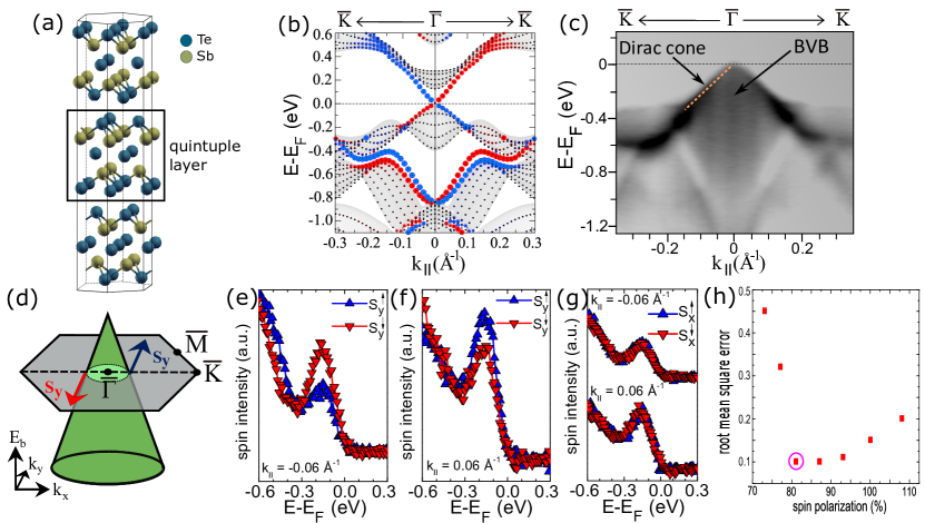
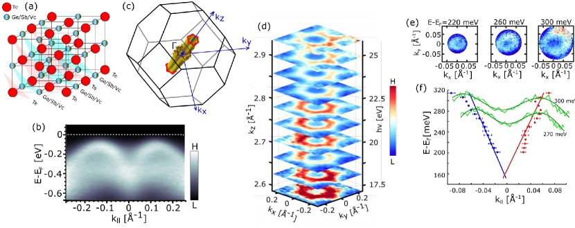
Soon after establishing 2DTIs experimentally [5] based on theoretical predictions [25], an extension of the formalism to 3D was proposed [24, 23]. It results in two types of 3D topological insulators (3DTIs). One exhibits an odd number of spin-helical TSSs on each surface and is dubbed strong 3DTI, while the other one has an even number of topological surface states on every surface except one and is dubbed weak 3DTI [24, 23]. After identifying a first strong 3DTI in a BiSb alloy by ARPES [28], DFT calculations predicted stoichiometric materials to be strong 3DTIs, namely Bi2Te3, Sb2Te3, and Bi2Se3 [30]. These three materials share the same crystal structure of quintuple layers (QL) that are stacked on each other by van-der-Waals forces (Fig. 1(a)). Hence, these materials can be cleaved in-situ and can be exfoliated as thin films [63, 64]. Moreover, they have been predicted to exhibit a single TSS on the cleavage plane with the Dirac point located in the center of the Brillouin zone at the so-called point (Fig. 1(b)) [30].
These properties enable a simple investigation by SARPES provided that the Dirac cone (TSS) is below . Indeed, the first ARPES measurements of a TSS on Bi2Se3(0001) have been published [65] back-to-back with the DFT based predictions [30]. First SARPES measurements appeared only three month later [29]. It turned out that the cleaved bulk samples of Bi2Se3 and Bi2Te3 are n-doped, being beneficial for the ARPES mapping of the TSS, but detrimental for electric transport. In contrast, Sb2Te3 is usually p-doped [66, 67] impeding ARPES mapping. Luckily, we obtained a twenty year old Sb2Te3 crystal that enabled mapping of the lower part of the Dirac cone via ARPES (Fig. 1(c)) [50]. This part of the Dirac cone encloses states of the bulk valence band in space in quantitative accordance with DFT calculations (Fig. 1(b)). Since the doping is caused by point defects of the material [68, 69], we speculate that the particular defect distribution within this material is responsible for establishing the favorable . Similar results exhibiting Dirac cones within the band gap close to have also been found for Sb2Te3, Bi2Se3, and Bi2Te3 after careful optimization of growth conditions in UHV [68, 70, 44].
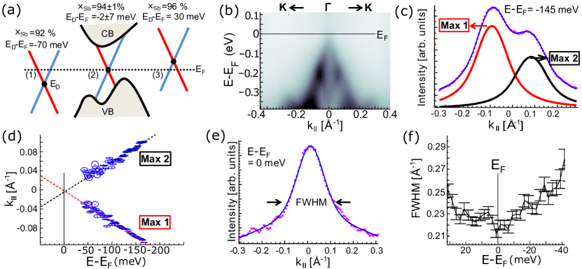
Figure 1(e)(g) show SARPES data recorded via a Mott detector, that probes the two in-plane directions of the spin. Two peaks at opposite are recorded corresponding to the two opposite sides of the Dirac cone. The spin polarization is found to be exclusively perpendicular to the vector as expected from the (Rashba-type) spin-orbit interaction. It is, moreover, helical, i.e., it switches sign when inverting . These are the typical fingerprints of a Dirac cone type TSS [30]. Out-of-plane spin polarizations have also been observed, in particular, further away from and are traced back to distortions of the simple Dirac cone, e.g., via warping, i.e., by influences of the crystal structure [72]. It is important to realize that SARPES does not probe the spin polarization of the initial state exclusively, but that the photoemission process is an excitation to unoccupied states extending into the vacuum that can change the spin polarization either by matrix effects or by spin polarization of the final state [73]. This can be captured by calculations within the so-called fully relativistic one-step model based on DFT calculations [74]. In particular, at low photon energies, it turns out that the detected spin polarization can even be inverted with respect to the initial state depending on the polarization direction of the exciting light [75]. At higher energies in the deep UV regime, this is less relevant, since excited states are well above the vacuum level. Hence, the helicity of the TSS can be deduced being counterclockwise for the lower part of the Dirac cone of Sb2Te3 (Fig. 1(d)). This is in accordance with the DFT calculations (Fig. 1(b)). The absolute value of the spin polarization of the TSS is not extracted directly from our SARPES data due to the limited angular and energy resolution. The reduced resolution during SARPES with respect to ARPES is caused by the low efficiency of the Mott detector. Novel approaches improve this efficiency considerably via spin dependent, conserving reflections of the photoelectrons at single crystals [76]. Hence, resolution can be much better, but such apparatus was not available during the measurements presented in Fig. 1. Consequently, spin polarization had to be extracted rather indirectly by carefully subtracting the inelastic background, the background originating from the also measured spin-polarized surface states at lower energy (visible in Fig. 1(b) at to eV), and the background from the overlapping, enclosed bulk states. Nevertheless, the accordingly best fit of the SARPES data revealed a spin polarization of the TSS of % (Fig. 1(g)) matching the DFT result of 90 % surprisingly well [50]. Obviously, the TSS is not 100 % spin-polarized, albeit it is spin-helical. This is a natural consequence of spin-orbit interaction, that strongly mixes the spin with orbital degrees of freedom via the heavy atoms involved. Thus, spin is not a good quantum number in these materials.
III Tuning the Dirac point energy
One main task after the experimental discovery of 3DTIs was to tune their Dirac point energy , that mostly turned out to be far away from [8]. Hence, literally speaking, the first 3DTIs were not even insulators in their interior. More importantly, the transport properties of the 3DTIs could not be probed without rendering the bulk of the material sufficiently insulating. A rather obvious, initial approach was to exploit the opposite p-type doping of Sb2Te3 and n-type doping of Bi2Te3 or Bi2Se3. Two main strategies have been pursued. Either, the two materials are mixed in a way such that they exhibit a similar density of acceptors and donors [78, 79]. This approach eventually led to the observation of the quantum Hall effect within thin films of BiSbTeSe2 as a clear signature of dominating 2D-type transport [80, 81]. Detailed analysis of the filling factor dependence of the Hall conductance identified the TSSs on bottom and top surface as the origin of the half integer quantum Hall effect [81]. The respective tuning of the Dirac cone, respectively , with respect to can be monitored by ARPES in detail [82]. This is particularly important for the protection of Majorana states within vortices of a topological superconductor against conventional single-particle excitations by an effective gap reading [83, 84, 85]
| (1) |
with being the excitation gap of the surrounding topological superconductor.
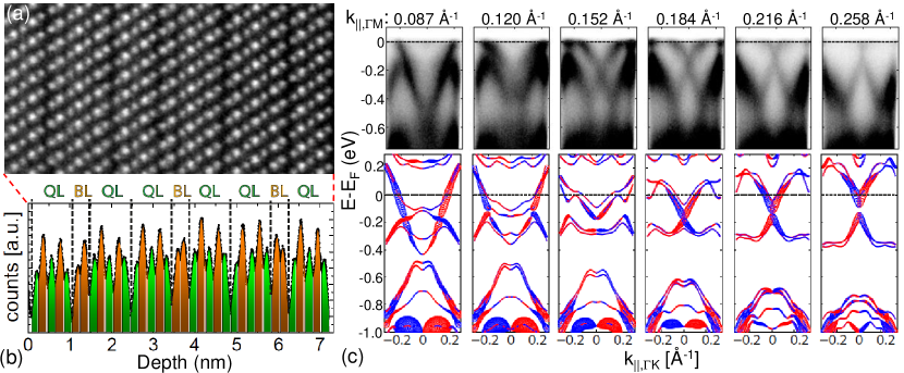
Figure 2(a) sketches the results for (BiSbTe3 at different mixing of Sb and Bi including the case of . Corresponding ARPES data are displayed in Fig. 2(b) [82, 71]. Figure 2(c)(f) shows the evaluation of the data. The values of the TSS are obtained from fitting intensity profiles (Fig. 2(c)) at different energies that are subsequently extrapolated linearly to determine the crossing point as (Fig. 2(d)). Alternatively, the full width at half maximum (FWHM) of closer to (Fig. 2(e)) is employed via identifying as the energy with lowest FWHM (Fig. 2(f)). In both cases, has to be carefully calibrated as well. For the particular sample, we found within 5 meV [71]. Since no time dependent band shifts were observed, the value is likely robust as long as the sample is in UHV. However, ex-situ Hall measurements on identically prepared samples exhibit a transition form p-type to n-type bulk conduction at much lower Sb concentration ( %) [87]. Hence, rescuing the precise tuning for electric devices requires additional efforts and investigations.
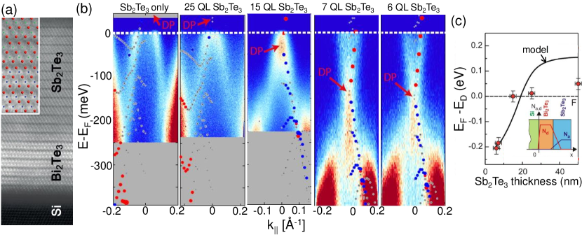
Another approach uses the electric field at interfaces between p-type and n-type 3DTIs [88, 77]. As well known for semiconductor p-n junctions, a depletion region forms at the interface such that a thin enough overlayer can maintain in the depletion region. This implies that remains in the band gap up to the surface. The approach has the general advantage that it avoids ternary or quarternary alloys that potentially induce additional scattering centers for electrons via alloying. Figure 3(a) displays a transmission electron microscope (TEM) image of a stack of n-type and p-type 3DTIs grown by molecular beam epitaxy (MBE). A relatively sharp interface is observed via the material contrast due to different atomic weights of Bi and Sb. Figure 3(b) shows ARPES data at different thickness of the upper p-type Sb2Te3 on n-type Bi2Te3. Obviously, the Dirac cone is shifted downwards in energy with decreasing Sb2Te3 thickness. This confirms the reasoning of an upwards shift at the surface via the depletion zone. To determine including the thicknesses, where it is above , DFT results of 6 QL Sb2Te3 are overlaid after rigidly shifting them to reproduce the ARPES data. It turned out that the best anchor point for shifting is the surface state at lower energy (Fig. 1(b) at to eV). This state is vertically stronger confined to the surface area and, hence, is more intense in ARPES and less prone to the averaging by the vertical band bending [50] (details in [77]). The resulting has been compared with the result of a 1D Poisson-Schrödinger model revealing reasonable agreement (Fig. 3(c)). The model is based on the charge carrier densities of MBE grown films of Sb2Te3 and Bi2Te3 as determined by Hall measurements, while assuming the same density of dopants and charge carriers. An intermixing at the interface is additionally taken into account that is deduced from Auger electron spectroscopy depth profiling [77]. Obviously, depletion method via p-n junction is also able to tune for a thickness of QL Sb2Te3 on top of Bi2Te3.
IV Materials with particular properties: Dual topological insulators and phase change materials
Dual topological insulators
Another important application of ARPES is to confirm desired properties of novel topological materials. This includes topologically crystalline insulators (TCIs) [90, 91], Dirac semimetals [92, 93, 94] and Weyl semimetals [95, 96]. Interestingly, topological properties of different kind can be combined in a single material, if the topological indices belong to different symmetries of the Hamiltonian [97]. For example, 3DTIs protected by time-reversal symmetry can be combined with TCIs protected by a crystal symmetry such as -fold rotation or mirroring [98]. This raises the perspective to break one of the symmetries, hence, switching between different topology types [97, 86]. The first material that experimentally showed dual topology was Bi1Te1 [86]. It consists of stacked Bi bilayers (BLs) and Bi2Te3 QLs in a ratio of as evidenced by TEM (Fig. 4(a)(b)). Bi BLs are well known to be 2DTIs [99, 100, 53] such that the stacking of such bilayers at sufficiently low interlayer interaction would result in a weak 3DTI. The so-called dark surface without TSS is simply the Bi BL surface, while the edge states of the BL lead to the TSSs at all other surfaces. The Bi2Te3 layers can be thought of as spacer layers between the Bi bilayers or as 2DTI layers themselves. Indeed, DFT calculations find a small band gap of 0.1 eV around for the intrinsic, i.e., undoped, Bi1Te1 with topological indices (0;001). This indicates a weak 3DTI with its dark surface perpendicular to the (001) direction [86]. However, the reasoning via stacked 2DTIs is too simple, when analyzing the DFT data in more detail. Interlayer hybridizations mix up the 2D bands strongly, such that the weak 3DTI properties are rather accidental and not directly related to the 2DTI properties of the constituting layers. Intriguingly, the mirror Chern number of the same gap around , that is protected by a mirror symmetry across the plane, is rendering the system a TCI as well. Consequently, one expects an additional pair of Dirac cones on the dark (001) surface of the weak 3DTI Bi1Te1. The Dirac points of these Dirac cones are necessarily located on the line in space where the (001) surface intersects with the mirror plane. It must, moreover, be offset in opposite directions from . Figure 4(c) (upper row) shows a set of ARPES data in representation that are recorded perpendicular to this mirror line for increasing values along the line. The data exhibit an apparent Dirac cone as crossing of two bands at Å-1 and eV. The development of the bands with towards the crossing agrees nicely with corresponding DFT results of Bi1Te1(001) (Fig. 4(c), lower row). In order to achieve this agreement, the Bi1Te1 film had to be terminated by a single QL and had to be downshifted by 100 meV with respect to , Both is reasonable with the latter accounting for n-type doping as expected from the well known n-type doping of Bi2Te3. The good agrement between ARPES and DFT data, also found for multiple other bands of Bi1Te1, is the central evidence for the dual topological character of Bi1Te1 [86].
Topological phase change materials
Another interesting class of 3DTI materials are commercially used in electronic applications. They are called phase change materials (PCMs) providing two favorable properties for data storage. Firstly, they are fastly switchable (ns-scale) between the amorphous and a metastable crystalline phase at low energy penalty [101, 102]. Secondly, they exhibit a strong difference in optical reflectivity and electric conductivity between the two phases [103]. Consequently, they are employed in DVDs and random-access memories [103]. A standard class of PCMs is found on the pseudobinary line between the strong 3DTI Sb2Te3 and GeTe [104]. The later material is also strongly influenced by spin-orbit interaction revealing a strongly Rashba-split surface state and a strongly Rashba-split bulk state at [105, 106, 107]. Hence, it is natural to assume that some of the PCMs are 3DTIs as well. Indeed, DFT predicts 3DTI properties [108, 109, 110, 111] and finds that the 3DTI character depends strongly on details of the atomic arrangement [110, 111]. Figure 5(a) shows the structure of the most commonly used PCM Ge2Sb2Te5 in its metastable phase. It consists of alternating layers of hexagonal Te and a mixture of Ge, Sb and vacancies. If these ABC stacked layers exhibit additional order in the Ge/Sb/vacancy layers depends on details of the preparation and is decisive for the 3DTI properties according to DFT [108, 109, 110, 111]. Hence, a subtle borderline between strong 3DTI and trivial properties appears. Based on these findings, it has even been speculated that the reversible, strong difference in electric conductivity of a superlattice GeTe/Sb2Te3, that appears after applying voltage pulses without making the material amorphous, is caused by a switch in topology [112, 113].
However, the experimental confirmation of strong 3DTI properties in PCMs is complicated by the p-type doping. Hence, initially the only evidence by ARPES was the M shaped valence band with maxima away from (Fig. 5(b)) [114]. This configuration has been found in DFT calculations only for inverted bands representing a strong 3DTI [108, 109, 110, 111]. The p-type character of these bands is unconventional, since the energetically highest peak position in plots is about 100 meV below (Fig. 5(b)). The p-type doping is instead realized by the tails of the disorder broadened valence bands that cut . Hence, the ARPES intensity at provides a distribution mimicking the highest energy peaks below (Fig. 5(c), (d)). This is called the pseudo Fermi surface that can indeed be used to deduce the charge carrier density in good agreement with Hall measurements, if adequately weighted by the broadening of the valence bands due to disorder [89]. Hence, disorder in the Ge/Sb/vacancy layer is the central ingredient for the conductivity of the metastable PCM phase [89].
The TSS above the broadened valence bands has been found by two-photon ARPES, i.e., a first light pulse transfers electrons into the initially unoccupied TSS and a second light pulse with time delay extracts photoelectrons from the now occupied TSS. Figure 5(e) shows data for several energies above exhibiting a rather isotropic circle in space. The circle shrinks in diameter with decreasing energy. Extrapolation of the radius to lower energies (Fig. 5(f)) implies vanishing diameter at about 160 meV above that represents . Hence, the well-established conducting phase of the PCM Ge2Sb2Te5 is a strong 3DTI, at least, after the preparation by MBE as probed in this study [89]. This is appealing for 3DTI-based applications via exploiting the established expertise for upscaling conventional Ge2Sb2Te5 devices [115]. Counteracting the unfavorable p-doping of Ge2Sb2Te5 is possible by replacement of Ge with the heavier Sn [116], where, however, 3DTI properties still have to be demonstrated experimentally [117].
V Disorder characterization
As described in the introduction, a central task for improving the electric transport properties of 3DTIs (and 2DTIs) is the reduction of disorder. Disorder can lead to additional transport channels concealing the features of the TSS as well as to scattering of the TSS electrons [8, 32]. STS is the tool of choice for probing the disorder at the surface due to its unprecedented spatial and energy resolution in probing the LDOS. It has only the minor drawback that it is exclusively measuring the surface disorder and not the disorder within deeper layers of the bulk of the crystal [118].
One possibility by STS is to track characteristic features of the energy dependent LDOS [43, 44]. One measures curves with being the tunnel current and being the voltage applied between tip and sample. Mostly, such curves are measured by lock-in technique, i.e., the tip-surface distance is stabilized at voltage and current . Afterwards, the feedback loop is switched off, such that the tip surface distance remains constant, while the voltage is changed linearly and overlapped with an oscillating voltage of amplitude that enables the phase sensitive detection of via a lock-in amplifier. In first order, the resulting represents the LDOS [119, 120, 121, 118]. This gives direct access, e.g., to spatial variations of the band gap for a semiconductor or insulator.
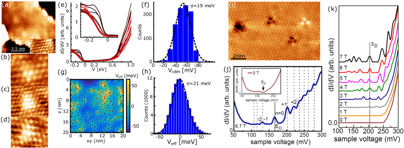
Figure 6(a) shows the (111) surface of the strong 3DTI Ge2Sb2Te5 exhibiting Te as the top layer with hexagonal atomic structure [45]. Several, largely triangular bright protrusions appear on top of the atomic lattice (Fig. 6(b)(d)). They have been identified as subsurface defects by comparison with DFT data [45]. The lateral size of the triangle increases with the depth of the defect below the surface. The particular sample grown by MBE exhibits a defect density of /cm2. This implies a potential disorder due to the positive charging of most of the defects, in particular, vacancies [114, 45, 122]. The curves (Fig. 6(e)) show a band gap of about 0.5 eV with the valence band onset being close to in agreement with optical absorption [123] and ARPES data (Fig. 5(b)), respectively. The band gap onset is spatially varying. It is quantified via the peak position of the numerically determined curves leading to a nearly Gaussian distribution of the spatially varying valence band onset with width of meV (Fig. 6(f)). We compare this with a simple model calculation randomly distributing positive point charges with a density identical to the charge carrier density determined by Hall measurements (Fig. 6(g)). This leads to potential fluctuations on the surface with the same width as in the experiment (Fig. 6(h)). It implies that the Coulomb centers of the charged acceptors (vacancies) dominate disorder in this sample. Interestingly, the LDOS does not vanish within the band gap (Fig. 6(e)) indicating the presence of in-gap surface states in agreement with the two-photon ARPES revealing a TSS (Fig. 5(f)).
Another possibility to map potential disorder is Landau level spectroscopy, however, requiring a magnetic field. It exploits the Dirac type spin chirality of the TSS implying a so called zeroth Landau level (LL0) that is tied to [124, 125]. Hence, tracking LL0 across the surface maps the potential disorder as seen by the TSS, i.e., averaged across some of the upper QLs [48, 47, 49]. The lateral spatial resolution of the method is largely given by the magnetic length [126]. Figure 6(i) shows STM data of in-situ cleaved Sb2Te3(0001) featuring a few defects that have been identified previously by comparison with DFT calculations as Sb substitutional in the upper Te layer (SbTe, bright) and vacancies in the Sb layer directly below the surface (VacSb, dark) [69]. We find a defect density of /cm2 with all apparent defects attributed to the upper QL [49]. Figure 6(j)-(k) show Landau level spectra recorded at two different locations of the sample. It is apparent that the energy of LL0 does not shift with field (Fig. 6(k)). Moreover, LL0 appears at the same energy as the minimum in curves at T. Finally, LL0 deviates by meV between the two probed areas indicating the potential fluctuations. We found that the deduced LL0 energy correlates with the local density of defects visible in the STM data (not shown) [49].
VI Edge states of weak topological insulators
Weak 3DTIs have initially barely been studied due to the wrong conjecture that they are unstable with respect to most type of perturbations [24]. More detailed studies, however, revealed that the only detrimental perturbation is a strong dimerization of adjacent layers along the surface normal of the dark surface leading to a doubling of the unit cell [128, 129]. Hence, also weak 3DTIs typically exhibit robust spin-helical surface states protected from backscattering. The most simple way to construct a weak 3DTI is stacking 2DTIs without interlayer interaction [24, 129]. This naturally implies that single-layer terraces on the dark surface are patches of 2DTIs that consequently must host one-dimensional topological edge states at its step edges. These edge states are spin helical and, hence, ideal conductors as long as time-reversal symmetry is not broken [130]. It turns out that such edge states appear generally for weak 3DTIs even if constructed differently [130]. This implies the possibility to scratch a network of ideal conductors into the surface of a weak 3DTI [54].
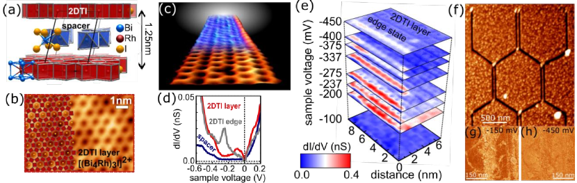
The first experimental realization of a weak 3DTI was Bi14Rh3I9 [131]. It consists of alternating layers of the 2DTI (Bi4Rh)3I [132] and the trivial insulator Bi2I8 (Fig. 7(a)). The 2DTI exhibits a honeycomb unit cell such as graphene, but is made of the heavy atoms Bi, I and Rh (Fig. 7(b)). It, thus, mimics the initial idea of a 2DTI in a honeycomb lattice [25], but provides a much stronger spin-orbit interaction ( eV) leading to a sizable inverted band gap of meV [132]. This gap is much larger than in graphene with inverted band gap of eV [133]. Hence, the idea to construct the 3D material is to stack 2DTI honeycomb structures [25] that are separated by trivial insulators as spacers impeding interactions between the 2DTI layers. However, it turned out that the strong spin-orbit interaction shifts much more bands across than only the initial Dirac cone of the honeycomb lattice that appears at without spin-orbit interaction [125]. Thus, the topological indices of a weak 3DTI again appear rather accidentally via inversion of several bands at the TRIMs of the Brillouin zone [132]. Nevertheless, topological edge states at each step edge are expected and have been found by STS. They are directly visible as enhanced LDOS intensity at step edges (Fig. 7(c), background). In curves, the band gap region of the material ( to eV) exhibits strong intensity exclusively at the step edges (Fig.7(d)). The edge states appear continuously along all edges [54] and are only nm wide perpendicular to the edge (Fig. 7(e)). Moreover, the edge states did not exhibit any fingerprints of standing waves, but only intensity modulations periodic with the unit cell as expected for Bloch states. Thus, backscattering is largely impeded. Networks of topological edge states can indeed be scratched into the surface either by the tip of an atomic force microscope (AFM) (Fig. 7(f)) with separation down to 25 nm [54] or by the tip of an STM. The resulting scratches indeed show an increased LDOS within the band gap (Fig.7(g)), but not at energies outside the gap (Fig. 7(h)).
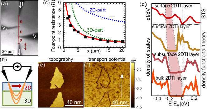
Unfortunately, is not within the band gap and, thus, the edge states are not accessible by electric transport. Four-tip STM measurements in UHV (Fig. 8(a)) [138], however, revealed that the resistance as a function of distance between the tips is not described by a 3D transport model only, but required a sizable contribution from a parallel 2D transport channel (Fig. 8(b)(c)). The best fit of the experimental data (red curve in Fig. 8(c), [134, 139]) implies conductances for the 2D and 3D contribution S and S/m, respectively. Thus, the 2D conductance corresponds to a m thick layer with the 3D conductance .
This implies that the surface region of Bi14Rh3I9 is significantly more conductive than the bulk. The encouraging finding is corroborated by DFT calculations of bulk Bi14Rh3I9 (Fig.8(d), bottom, orange curve) showing within the band gap. Additional calculations of a thin film revealed that the surface is strongly n-doped (Fig.8(d), yellow curve) with the band gap at similar energies as found in the STS data (Fig.8(d), top, red curve) [137]. This is in line with the strong 2D conductivity found by 4-tip STM. The band gap favorably moves quickly towards its bulk position already for the subsurface layer (Fig.8(d), pink curve). To explain the surface n-doping, we consider the charging of the individual layers. It turns out that the 2DTI layer (Bi4Rh)3I transfers about one electron per unit cell to each of its neighboring spacer layers Bi2I8 such that it is positively charged by about 2 electrons per unit cell in equilibrium. Under these circumstances, is in the band gap of the 2DTI layer. At the surface, however, one neighboring spacer layer is missing, such that about one electron per unit cell remains on the 2DTI layer making it strongly n-doped [137]. In principle, this could be counteracted by adding acceptors such as iodine onto the surface, but a relatively large amount of about one iodine atom per unit cell is required [140].
Using the four-tip STM, we also performed scanning tunneling potentiometry [141]. This method measures the tip voltage that is required to nullify the current between tip and sample. Consequently, it maps the local potential, typically while current is flowing laterally. With four-tip STM, two tips can be used to inject the current, while a third tip is scanned in between to probe the nullifying voltage [142, 138]. Consequently, the current induced potential is mapped. Figure 8(e) shows an area of the surface with 2DTI only, i.e., the islands exhibit step edges with height of a combined 2DTI and spacer layer. The potentiometry data show a barely visible overall decrease of the potential from the bottom to the top by about 0.1 mV due to the transport resistance. Much stronger features appear at the step edges and as patches on the surface of the 2DTI layers. They are identically present without applying current and are, hence, a static feature of the surface. Such features are caused by thermo-voltage resulting from a temperature difference of tip and sample K and, as such, indicate spatially different slopes of the LDOS at according to [143, 144]. As a result, the method reveals fluctuations of LDOS() on the 2DTI terraces and a significant difference between step edges and terraces. The experiment did not provide any indication of preferred transport along the step edges in agreement with the observation that the topological edge states are not at .
Other weak 3DTIs have been found [55, 56, 145, 146], but none with in the topological band gap. Some uncertainty remains for ZrTe5, that is very close to a topological phase transition such that details on strain and temperature change the topological properties partly also in a favorable way [147]. More interestingly, bismuthene, a honeycomb Bi monolayer on SiC(0001), is a 2DTI that can be prepared in UHV with inside the topological band gap of size eV [59]. Here, preferential transport along step edges might be detected by four-tip scanning tunneling potentiometry. Also the ideal conductance of the edge state could be probed. It would lead to a potential drop that only appears at the end of the step edge, i.e., at the transition to the terrace in current direction [148].
VII Conclusions
In this article, we summarized some of the key contributions of surface science methods to the development of 3DTIs. Most importantly, ARPES could identify strong 3DTIs via the Dirac cone and its spin helicity of the topological surface state, while STS could identify weak 3DTIs via their helical edge states protected from backscattering at the dark surface. Moreover, ARPES was instrumental to monitor the tuning of the Dirac cone towards , albeit the results are not compatible yet with the results from electric transport likely due to different treatment of the surfaces. Complementary, STS can map the potential disorder, most precisely via Landau level spectroscopy, and, hence, can monitor efforts to improve sample homogeneity. We have also shown exemplarily that particularly interesting materials can be identified as topological. In detail, we have discovered the first dual 3DTI Bi1Te1 and strong 3DTI properties in phase change materials as an example material used in commercial applications. Two-photon ARPES was crucial to find the Dirac cone in these materials that only appeared in the occupied states due to strong p-doping. Finally, we have introduced the abilities of four-tip STM that can provide electric transport data in UHV without the requirement of ex-situ contacting. We anticipate that this method will be perspectively important to adapt the results from ARPES and STS to electric transport and, hence, to devices, since different surface treatments, that lead, e.g., to contaminations due to lithography, can be avoided.
VIII acknowledgement
We strongly appreciate the previous contributions to the publications reviewed in this manuscript by P. Bhaskar, S. Blügel, S. Borisenko, J.E. Boschker, V. Bragaglia, R. Callarco, S. Checchi, N. Demarina, V. L. Deringer, S. Döring, R. Dronskowski, Th. Fauster, M. Gehlmann, A. Georgi, E. Golias, P. Gospodaric, M. Grob, D. Grützmacher, A. Guissani, C. Holl, B. Holländer, J. Kampmeier, B. Kaufmann, K. Koepernik, P. Küppers, M. Lanius, M. Luysberg, E. Mlynczak, E. Neumann, C. Niu, O. Rader, J. Sanchez-Barriga, T. Schäpers, C.M. Schneider, M.R. Scholz, P. Schüffelgen, D. Subramaniam, J. van den Brink, A. Varykhalov, R. N. Wang, and C. Weyrich. We, moreover, gratefully acknowledge funding by the Deutsche Forschungsgemeinschaft (DFG, German Research Foundation) via the project Mo 858/13-2 within the priority programme SPP1666 ”Topological Insulators” and via the Strategy Clusters of Excellence ”Matter and Light for Quantum Computing (ML4Q)” EXC 2004/1 390534769 as well as ”Complexity and Topology in Quantum Matter (ct.qmat)” ExC 2147, project-id 39085-490.
References
- [1] D. J. Thouless, M. Kohmoto, M. P. Nightingale, and M. den Nijs, Quantized Hall conductance in a two-dimensional periodic potential, Phys. Rev. Lett. 49(6), 405–408 (1982).
- [2] Q. Niu, D. J. Thouless, and Y. S. Wu, Quantized Hall conductance as a topological invariant, Phys. Rev. B 31(6), 3372–3377 (1985).
- [3] A. Cho, Updated: Trio snares physics Nobel for describing exotic states of matter, Science(October) (2016).
- [4] M. den Nijs David Thouless (19342019), Science 364(6443), 835–835 (2019).
- [5] M. König, S. Wiedmann, C. Brune, A. Roth, H. Buhmann, L. W. Molenkamp, X. L. Qi, and S. C. Zhang, Quantum spin Hall insulator state in HgTe quantum wells, Science 318(5851), 766–770 (2007).
- [6] M. Z. Hasan and C. L. Kane, Colloquium: Topological insulators, Rev. Mod. Phys. 82(4), 3045–3067 (2010).
- [7] X. L. Qi and S. C. Zhang, Topological insulators and superconductors, Rev. Mod. Phys. 83(4), 1057–1110 (2011).
- [8] Y. Ando, Topological insulator materials, J. Phys. Soc. Jp. 82(10), 102001 (2013).
- [9] B. Bahari, A. Ndao, F. Vallini, A. E. Amili, Y. Fainman, and B. Kanté, Nonreciprocal lasing in topological cavities of arbitrary geometries, Science 358(6363), 636–640 (2017).
- [10] J. Cha, K. W. Kim, and C. Daraio, Experimental realization of on-chip topological nanoelectromechanical metamaterials, Nature 564(7735), 229–233 (2018).
- [11] Y. Yang, Z. Gao, H. Xue, L. Zhang, M. He, Z. Yang, R. Singh, Y. Chong, B. Zhang, and H. Chen, Realization of a three-dimensional photonic topological insulator, Nature 565(7741), 622–626 (2019).
- [12] J. Ningyuan, C. Owens, A. Sommer, D. Schuster, and J. Simon, Time- and site-resolved dynamics in a topological circuit, Phys. Rev. X 5(2), 021031 (2015).
- [13] X. Zhang, J. Wang, and S. C. Zhang, Topological insulators for high-performance terahertz to infrared applications, Phys. Rev. B 82(24), 245107 (2010).
- [14] L. He, X. Kou, and K. L. Wang, Review of 3D topological insulator thin-film growth by molecular beam epitaxy and potential applications, phys. stat. sol. (RRL) 7(1-2), 50–63 (2013).
- [15] J. Han, A. Richardella, S. A. Siddiqui, J. Finley, N. Samarth, and L. Liu, Room-temperature spin-orbit torque switching induced by a topological insulator, Phys. Rev. Lett. 119(7), 077702 (2017).
- [16] J. Alicea, New directions in the pursuit of Majorana fermions in solid state systems, Rep. Prog. Phys. 75(7), 076501 (2012).
- [17] S. D. Sarma, M. Freedman, and C. Nayak, Majorana zero modes and topological quantum computation, Npj Quantum Inf. 1(1), 15001 (2015).
- [18] J. Alicea and P. Fendley, Topological phases with parafermions: theory and blueprints, Annual Review of Condensed Matter Physics 7(1), 119–139 (2016).
- [19] V. Lahtinen and J. Pachos, A short introduction to topological quantum computation, SciPost Phys. 3(3), 021 (2017).
- [20] T. Zhang, Y. Jiang, Z. Song, H. Huang, Y. He, Z. Fang, H. Weng, and C. Fang, Catalogue of topological electronic materials, Nature 566(7745), 475–479 (2019).
- [21] M. G. Vergniory, L. Elcoro, C. Felser, N. Regnault, B. A. Bernevig, and Z. Wang, A complete catalogue of high-quality topological materials, Nature 566(7745), 480–485 (2019).
- [22] J. E. Moore and L. Balents, Topological invariants of time-reversal-invariant band structures, Phys. Rev. B 75(12), 121306 (2007).
- [23] L. Fu, C. L. Kane, and E. J. Mele, Topological insulators in three dimensions, Phys. Rev. Lett. 98(10), 106803 (2007).
- [24] L. Fu and C. L. Kane, Topological insulators with inversion symmetry, Phys. Rev. B 76(4), 045302 (2007).
- [25] C. L. Kane and E. J. Mele, topological order and the quantum spin hall effect, Phys. Rev. Lett. 95(Sep), 146802 (2005).
- [26] N. Mardirossian and M. Head-Gordon, Thirty years of density functional theory in computational chemistry: an overview and extensive assessment of 200 density functionals, Mol. Phys. 115(19), 2315–2372 (2017).
- [27] M. Stöhr, T. V. Voorhis, and A. Tkatchenko, Theory and practice of modeling van der Waals interactions in electronic-structure calculations, Chem. Soc. Rev. 48(15), 4118–4154 (2019).
- [28] D. Hsieh, D. Qian, L. Wray, Y. Xia, Y. S. Hor, R. J. Cava, and M. Z. Hasan, A topological Dirac insulator in a quantum spin Hall phase, Nature 452(7190), 970–974 (2008).
- [29] D. Hsieh, Y. Xia, L. Wray, D. Qian, A. Pal, J. H. Dil, J. Osterwalder, F. Meier, G. Bihlmayer, C. L. Kane, Y. S. Hor, R. J. Cava, and M. Z. Hasan, Observation of unconventional quantum spin textures in topological insulators, Science 323(5916), 919–922 (2009).
- [30] H. Zhang, C. X. Liu, X. L. Qi, X. Dai, Z. Fang, and S. C. Zhang, Topological insulators in Bi2Se3, Bi2Te3 and Sb2Te3 with a single Dirac cone on the surface, Nat. Phys. 5(6), 438–442 (2009).
- [31] D. Hsieh, Y. Xia, D. Qian, L. Wray, J. H. Dil, F. Meier, J. Osterwalder, L. Patthey, J. G. Checkelsky, N. P. Ong, A. V. Fedorov, H. Lin, A. Bansil, D. Grauer, Y. S. Hor, R. J. Cava, and M. Z. Hasan, A tunable topological insulator in the spin helical Dirac transport regime, Nature 460(7259), 1101–1105 (2009).
- [32] D. Culcer, Transport in three-dimensional topological insulators: theory and experiment, Physica E 44(5), 860–884 (2012).
- [33] B. Yan, D. Zhang, and C. Felser, Topological surface states of Bi2Se3 coexisting with Se vacancies, phys. stat. sol. (RRL) 7(1-2), 148–150 (2012).
- [34] P. Cheng, C. Song, T. Zhang, Y. Zhang, Y. Wang, J. F. Jia, J. Wang, Y. Wang, B. F. Zhu, X. Chen, X. Ma, K. He, L. Wang, X. Dai, Z. Fang, X. Xie, X. L. Qi, C. X. Liu, S. C. Zhang, and Q. K. Xue, Landau quantization of topological surface states in Bi2Se3, Phys. Rev. Lett. 105(7), 076801 (2010).
- [35] T. R. Devidas, E. P. Amaladass, S. Sharma, R. Rajaraman, D. Sornadurai, N. Subramanian, A. Mani, C. S. Sundar, and A. Bharathi, Role of Se vacancies on Shubnikov-de Haas oscillations in Bi2Se3: a combined magneto-resistance and positron annihilation study, Europhys. Lett. 108(6), 67008 (2014).
- [36] M. Bianchi, D. Guan, S. Bao, J. Mi, B. B. Iversen, P. D. King, and P. Hofmann, Coexistence of the topological state and a two-dimensional electron gas on the surface of Bi2Se3, Nat. Commun. 1(1), 128 (2010).
- [37] P. D. C. King, R. C. Hatch, M. Bianchi, R. Ovsyannikov, C. Lupulescu, G. Landolt, B. Slomski, J. H. Dil, D. Guan, J. L. Mi, E. D. L. Rienks, J. Fink, A. Lindblad, S. Svensson, S. Bao, G. Balakrishnan, B. B. Iversen, J. Osterwalder, W. Eberhardt, F. Baumberger, and P. Hofmann, Large tunable Rashba spin splitting of a two-dimensional electron gas in Bi2Se3, Phys. Rev. Lett. 107(9), 096802 (2011).
- [38] E. Frantzeskakis, S. Ramankutty, N. de Jong, Y. Huang, Y. Pan, A. Tytarenko, M. Radovic, N. Plumb, M. Shi, A. Varykhalov, A. de Visser, E. van Heumen, and M. Golden, Trigger of the ubiquitous surface band bending in 3D topological insulators, Phys. Rev. X 7(4), 041041 (2017).
- [39] B. Skinner, T. Chen, and B. I. Shklovskii, Why is the bulk resistivity of topological insulators so small?, Phys. Rev. Lett. 109(17), 176801 (2012).
- [40] N. Borgwardt, J. Lux, I. Vergara, Z. Wang, A. A. Taskin, K. Segawa, P. H. M. van Loosdrecht, Y. Ando, A. Rosch, and M. Grüninger, Self-organized charge puddles in a three-dimensional topological material, Phys. Rev. B 93(24), 245149 (2016).
- [41] M. Morgenstern, C. Wittneven, R. Dombrowski, and R. Wiesendanger, Spatial fluctuations of the density of states in magnetic fields observed with scanning tunneling spectroscopy, Phys. Rev. Lett. 84(24), 5588–5591 (2000).
- [42] M. Morgenstern, J. Klijn, C. Meyer, M. Getzlaff, R. Adelung, R. A. Römer, K. Rossnagel, L. Kipp, M. Skibowski, and R. Wiesendanger, Direct comparison between potential landscape and local density of states in a disordered two-dimensional electron system, Phys. Rev. Lett. 89(13), 136806 (2002).
- [43] H. Beidenkopf, P. Roushan, J. Seo, L. Gorman, I. Drozdov, Y. S. Hor, R. J. Cava, and A. Yazdani, Spatial fluctuations of helical Dirac fermions on the surface of topological insulators, Nat. Phys. 7(12), 939–943 (2011).
- [44] J. Dai, D. West, X. Wang, Y. Wang, D. Kwok, S. W. Cheong, S. Zhang, and W. Wu, Toward the intrinsic limit of the topological insulator Bi2Se3, Phys. Rev. Lett. 117(10), 106401 (2016).
- [45] J. Kellner, G. Bihlmayer, V. L. Deringer, M. Liebmann, C. Pauly, A. Giussani, J. E. Boschker, R. Calarco, R. Dronskowski, and M. Morgenstern, Exploring the subsurface atomic structure of the epitaxially grown phase-change material Ge2Sb2Te5, Phys. Rev. B 96(24), 245408 (2017).
- [46] T. Hanaguri, K. Igarashi, M. Kawamura, H. Takagi, and T. Sasagawa, Momentum-resolved Landau-level spectroscopy of dirac surface state in Bi2Se3, Phys. Rev. B 82(8), 081305 (2010).
- [47] Y. S. Fu, M. Kawamura, K. Igarashi, H. Takagi, T. Hanaguri, and T. Sasagawa, Imaging the two-component nature of Dirac Landau levels in the topological surface state of Bi2Se3, Nature Physics 10(11), 815–819 (2014).
- [48] Y. Okada, W. Zhou, C. Dhital, D. Walkup, Y. Ran, Z. Wang, S. D. Wilson, and V. Madhavan, Visualizing Landau levels of Dirac electrons in a one-dimensional potential, Phys. Rev. Lett. 109(16), 166407 (2012).
- [49] C. Pauly, C. Saunus, M. Liebmann, and M. Morgenstern, Spatially resolved Landau level spectroscopy of the topological Dirac cone of bulk-type Sb2Te3(0001): potential fluctuations and quasiparticle lifetime, Phys. Rev. B 92(8), 085140 (2015).
- [50] C. Pauly, G. Bihlmayer, M. Liebmann, M. Grob, A. Georgi, D. Subramaniam, M. R. Scholz, J. Sánchez-Barriga, A. Varykhalov, S. Blügel, O. Rader, and M. Morgenstern, Probing two topological surface bands of Sb2Te3 by spin-polarized photoemission spectroscopy, Phys. Rev. B 86(23), 235106 (2012).
- [51] A. Takayama, T. Sato, S. Souma, T. Oguchi, and T. Takahashi, One-dimensional edge states with giant spin splitting in a bismuth thin film, Phys. Rev. Lett. 114(6), 066402 (2015).
- [52] M. Bianchi, F. Song, S. Cooil, Å. F. Monsen, E. Wahlström, J. A. Miwa, E. D. L. Rienks, D. A. Evans, A. Strozecka, J. I. Pascual, M. Leandersson, T. Balasubramanian, P. Hofmann, and J. W. Wells, One-dimensional spin texture of Bi(441): Quantum spin Hall properties without a topological insulator, Phys. Rev. B 91(16), 165307 (2015).
- [53] I. K. Drozdov, A. Alexandradinata, S. Jeon, S. Nadj-Perge, H. Ji, R. J. Cava, B. A. Bernevig, and A. Yazdani, One-dimensional topological edge states of bismuth bilayers, Nat. Phys. 10(9), 664–669 (2014).
- [54] C. Pauly, B. Rasche, K. Koepernik, M. Liebmann, M. Pratzer, M. Richter, J. Kellner, M. Eschbach, B. Kaufmann, L. Plucinski, C. M. Schneider, M. Ruck, J. van den Brink, and M. Morgenstern, Subnanometre-wide electron channels protected by topology, Nat. Phys. 11(4), 338–343 (2015).
- [55] X. B. Li, W. K. Huang, Y. Y. Lv, K. W. Zhang, C. L. Yang, B. B. Zhang, Y. Chen, S. H. Yao, J. Zhou, M. H. Lu, L. Sheng, S. C. Li, J. F. Jia, Q. K. Xue, Y. F. Chen, and D. Y. Xing, Experimental observation of topological edge states at the surface step edge of the topological insulator ZrTe5, Phys. Rev. Lett. 116(17), 176803 (2016).
- [56] R. Wu, J. Z. Ma, S. M. Nie, L. X. Zhao, X. Huang, J. X. Yin, B. B. Fu, P. Richard, G. F. Chen, Z. Fang, X. Dai, H. M. Weng, T. Qian, H. Ding, and S. Pan, Evidence for topological edge states in a large energy gap near the step edges on the surface of ZrTe5, Phys. Rev. X 6(2), 021017 (2016).
- [57] P. Sessi, D. D. Sante, A. Szczerbakow, F. Glott, S. Wilfert, H. Schmidt, T. Bathon, P. Dziawa, M. Greiter, T. Neupert, G. Sangiovanni, T. Story, R. Thomale, and M. Bode, Robust spin-polarized midgap states at step edges of topological crystalline insulators, Science 354(6317), 1269–1273 (2016).
- [58] L. Peng, Y. Yuan, G. Li, X. Yang, J. J. Xian, C. J. Yi, Y. G. Shi, and Y. S. Fu, Observation of topological states residing at step edges of WTe2, Nat. Commun. 8(1), 659 (2017).
- [59] F. Reis, G. Li, L. Dudy, M. Bauernfeind, S. Glass, W. Hanke, R. Thomale, J. Schäfer, and R. Claessen, Bismuthene on a SiC substrate: A candidate for a high-temperature quantum spin Hall material, Science 357(6348), 287–290 (2017).
- [60] C. Meyer, J. Klijn, M. Morgenstern, and R. Wiesendanger, Direct measurement of the local density of states of a disordered one-dimensional conductor, Phys. Rev. Lett. 91(7), 076803 (2003).
- [61] S. H. Kim, K. H. Jin, J. Park, J. S. Kim, S. H. Jhi, and H. W. Yeom, Topological phase transition and quantum spin Hall edge states of antimony few layers, Sci. Rep. 6(1), 33193 (2016).
- [62] A. Bansil, H. Lin, and T. Das, Colloquium: topological band theory, Rev. Mod. Phys. 88(2), 021004 (2016).
- [63] B. Lampert and K. Reichelt, The investigation of cleavage faces and evaporated cleavage faces of Sb2Te3 by surface decoration, J. Cryst.l Growth 51(2), 203–212 (1981).
- [64] D. Teweldebrhan, V. Goyal, and A. A. Balandin, Exfoliation and characterization of bismuth telluride atomic quintuples and quasi-two-dimensional crystals, Nano Lett. 10(4), 1209–1218 (2010).
- [65] Y. Xia, D. Qian, D. Hsieh, L. Wray, A. Pal, H. Lin, A. Bansil, D. Grauer, Y. S. Hor, R. J. Cava, and M. Z. Hasan, Observation of a large-gap topological-insulator class with a single Dirac cone on the surface, Nat. Phys. 5(6), 398–402 (2009).
- [66] D. Hsieh, Y. Xia, D. Qian, L. Wray, F. Meier, J. H. Dil, J. Osterwalder, L. Patthey, A. V. Fedorov, H. Lin, A. Bansil, D. Grauer, Y. S. Hor, R. J. Cava, and M. Z. Hasan, Observation of time-reversal-protected single-dirac-cone topological-insulator states in Bi2Te3 and Sb2Te3, Phys. Rev. Lett. 103(14), 146401 (2009).
- [67] C. Seibel, H. Maaß, H. Bentmann, J. Braun, K. Sakamoto, M. Arita, K. Shimada, J. Minár, H. Ebert, and F. Reinert, The Rashba-split surface state of Sb2Te3(0001) and its interaction with bulk states, J. Electr. Spectr. Rel. Phen. 201(May), 110–114 (2015).
- [68] G. Wang, X. Zhu, J. Wen, X. Chen, K. He, L. Wang, X. Ma, Y. Liu, X. Dai, Z. Fang, J. Jia, and Q. Xue, Atomically smooth ultrathin films of topological insulator Sb2Te3, Nano Res. 3(12), 874–880 (2010).
- [69] Y. Jiang, Y. Y. Sun, M. Chen, Y. Wang, Z. Li, C. Song, K. He, L. Wang, X. Chen, Q. K. Xue, X. Ma, and S. B. Zhang, Fermi-level tuning of epitaxial Sb2Te3 thin films on graphene by regulating intrinsic defects and substrate transfer doping, Phys. Rev. Lett. 108(6), 066809 (2012).
- [70] K. Hoefer, C. Becker, D. Rata, J. Swanson, P. Thalmeier, and L. H. Tjeng, Intrinsic conduction through topological surface states of insulating Bi2Te3 epitaxial thin films, Proc. Nat. Acad. Sci. 111(42), 14979–14984 (2014).
- [71] J. Kellner, M. Eschbach, J. Kampmeier, M. Lanius, E. Młyńczak, G. Mussler, B. Holländer, L. Plucinski, M. Liebmann, D. Grützmacher, C. M. Schneider, and M. Morgenstern, Tuning the dirac point to the Fermi level in the ternary topological insulator (Bi1-xSbx)2Te3, Appl. Phys. Lett. 107(25), 251603 (2015).
- [72] S. Souma, K. Kosaka, T. Sato, M. Komatsu, A. Takayama, T. Takahashi, M. Kriener, K. Segawa, and Y. Ando, Direct measurement of the out-of-plane spin texture in the Dirac-cone surface state of a topological insulator, Phys. Rev. Lett. 106(21), 216803 (2011).
- [73] S. Hüfner, Photoelectron Spectroscopy (Springer Berlin Heidelberg, 1995).
- [74] H. Ebert, D. Ködderitzsch, and J. Minár, Calculating condensed matter properties using the KKR-Greens function methodrecent developments and applications, Rep. Prog. Phys. 74(9), 096501 (2011).
- [75] C. Jozwiak, C. H. Park, K. Gotlieb, C. Hwang, D. H. Lee, S. G. Louie, J. D. Denlinger, C. R. Rotundu, R. J. Birgeneau, Z. Hussain, and A. Lanzara, Photoelectron spin-flipping and texture manipulation in a topological insulator, Nat. Phys. 9(5), 293–298 (2013).
- [76] K. Medjanik, O. Fedchenko, S. Chernov, D. Kutnyakhov, M. Ellguth, A. Oelsner, B. Schönhense, T. R. F. Peixoto, P. Lutz, C. H. Min, F. Reinert, S. Däster, Y. Acremann, J. Viefhaus, W. Wurth, H. J. Elmers, and G. Schönhense Direct 3D mapping of the Fermi surface and Fermi velocity, Nat. Mater. 16(6), 615–621 (2017).
- [77] M. Eschbach, E. Młyńczak, J. Kellner, J. Kampmeier, M. Lanius, E. Neumann, C. Weyrich, M. Gehlmann, P. Gospodarič, S. Döring, G. Mussler, N. Demarina, M. Luysberg, G. Bihlmayer, T. Schäpers, L. Plucinski, S. Blügel, M. Morgenstern, C. M. Schneider, and D. Grützmacher, Realization of a vertical topological p–n junction in epitaxial Sb2Te3/Bi2Te3 heterostructures, Nat. Commun. 6(1), 8816 (2015).
- [78] Z. Ren, A. A. Taskin, S. Sasaki, K. Segawa, and Y. Ando, Large bulk resistivity and surface quantum oscillations in the topological insulator Bi2Te2Se, Phys. Rev. B 82(24), 241306 (2010).
- [79] D. Kong, Y. Chen, J. J. Cha, Q. Zhang, J. G. Analytis, K. Lai, Z. Liu, S. S. Hong, K. J. Koski, S. K. Mo, Z. Hussain, I. R. Fisher, Z. X. Shen, and Y. Cui, Ambipolar field effect in the ternary topological insulator (BixSb1-x)2Te3 by composition tuning, Nat. Nanotechnol. 6(11), 705–709 (2011).
- [80] Y. Xu, I. Miotkowski, C. Liu, J. Tian, H. Nam, N. Alidoust, J. Hu, C. K. Shih, M. Z. Hasan, and Y. P. Chen, Observation of topological surface state quantum Hall effect in an intrinsic three-dimensional topological insulator, Nat. Phys. 10(12), 956–963 (2014).
- [81] Y. Xu, I. Miotkowski, and Y. P. Chen, Quantum transport of two-species Dirac fermions in dual-gated three-dimensional topological insulators, Nat. Commun. 7(1), 11434 (2016).
- [82] J. Zhang, C. Z. Chang, Z. Zhang, J. Wen, X. Feng, K. Li, M. Liu, K. He, L. Wang, X. Chen, Q. K. Xue, X. Ma, and Y. Wang, Band structure engineering in (Bi1-xSbx)2Te3 ternary topological insulators, Nat. Commun. 2(1), 574 (2011).
- [83] J. D. Sau, R. M. Lutchyn, S. Tewari, and S. D. Sarma, Robustness of Majorana fermions in proximity-induced superconductors, Phys. Rev. B 82(9), 094522 (2010).
- [84] A. L. Rakhmanov, A. V. Rozhkov, and F. Nori, Majorana fermions in pinned vortices, Phys. Rev. B 84(7), 075141 (2011).
- [85] J. P. Xu, C. Liu, M. X. Wang, J. Ge, Z. L. Liu, X. Yang, Y. Chen, Y. Liu, Z. A. Xu, C. L. Gao, D. Qian, F. C. Zhang, and J. F. Jia, Artificial topological superconductor by the proximity effect, Phys. Rev. Lett. 112(21), 217001 (2014).
- [86] M. Eschbach, M. Lanius, C. Niu, E. Młyńczak, P. Gospodarič, J. Kellner, P. Schüffelgen, M. Gehlmann, S. Döring, E. Neumann, M. Luysberg, G. Mussler, L. Plucinski, M. Morgenstern, D. Grützmacher, G. Bihlmayer, S. Blügel, and C. M. Schneider, Bi1Te1 is a dual topological insulator, Nat. Commun.s 8(1), 14976 (2017).
- [87] C. Weyrich, M. Drögeler, J. Kampmeier, M. Eschbach, G. Mussler, T. Merzenich, T. Stoica, I. E. Batov, J. Schubert, L. Plucinski, B. Beschoten, C. M. Schneider, C. Stampfer, D. Grützmacher, and T. Schäpers, Growth, characterization, and transport properties of ternary (Bi1-xSbx)2Te3 topological insulator layers, J. Phys.: Cond. Mat. 28(49), 495501 (2016).
- [88] J. Wang, X. Chen, B. F. Zhu, and S. C. Zhang, Topologicalp-njunction, Phys. Rev. B 85(23), 235131 (2012).
- [89] J. Kellner, G. Bihlmayer, M. Liebmann, S. Otto, C. Pauly, J. E. Boschker, V. Bragaglia, S. Cecchi, R. N. Wang, V. L. Deringer, P. Küppers, P. Bhaskar, E. Golias, J. Sánchez-Barriga, R. Dronskowski, T. Fauster, O. Rader, R. Calarco, and M. Morgenstern, Mapping the band structure of GeSbTe phase change alloys around the Fermi level, Commun. Phys. 1(1), 5 (2018).
- [90] Y. Tanaka, Z. Ren, T. Sato, K. Nakayama, S. Souma, T. Takahashi, K. Segawa, and Y. Ando, Experimental realization of a topological crystalline insulator in SnTe, Nat. Phys. 8(11), 800–803 (2012).
- [91] P. Dziawa, B. J. Kowalski, K. Dybko, R. Buczko, A. Szczerbakow, M. Szot, E. Łusakowska, T. Balasubramanian, B. M. Wojek, M. H. Berntsen, O. Tjernberg, and T. Story, Topological crystalline insulator states in Pb1-xSnxSe, Nat. Mater. 11(12), 1023–1027 (2012).
- [92] Z. K. Liu, B. Zhou, Y. Zhang, Z. J. Wang, H. M. Weng, D. Prabhakaran, S. K. Mo, Z. X. Shen, Z. Fang, X. Dai, Z. Hussain, and Y. L. Chen, Discovery of a three-dimensional topological Dirac semimetal, Na3Bi, Science 343(6173), 864–867 (2014).
- [93] Z. K. Liu, J. Jiang, B. Zhou, Z. J. Wang, Y. Zhang, H. M. Weng, D. Prabhakaran, S. K. Mo, H. Peng, P. Dudin, T. Kim, M. Hoesch, Z. Fang, X. Dai, Z. X. Shen, D. L. Feng, Z. Hussain, and Y. L. Chen, A stable three-dimensional topological Dirac semimetal Cd3As2, Nat. Mater. 13(7), 677–681 (2014).
- [94] M. Yan, H. Huang, K. Zhang, E. Wang, W. Yao, K. Deng, G. Wan, H. Zhang, M. Arita, H. Yang, Z. Sun, H. Yao, Y. Wu, S. Fan, W. Duan, and S. Zhou, Lorentz-violating type-II Dirac fermions in transition metal dichalcogenide PtTe2, Nat. Commun. 8(1), 257 (2017).
- [95] S. Y. Xu, I. Belopolski, N. Alidoust, M. Neupane, G. Bian, C. Zhang, R. Sankar, G. Chang, Z. Yuan, C. C. Lee, S. M. Huang, H. Zheng, J. Ma, D. S. Sanchez, B. Wang, A. Bansil, F. Chou, P. P. Shibayev, H. Lin, S. Jia, and M. Z. Hasan, Discovery of a Weyl fermion semimetal and topological fermi arcs, Science 349(6248), 613–617 (2015).
- [96] B. Lv, H. Weng, B. Fu, X. Wang, H. Miao, J. Ma, P. Richard, X. Huang, L. Zhao, G. Chen, Z. Fang, X. Dai, T. Qian, and H. Ding, Experimental discovery of Weyl semimetal TaAs, Phys. Rev. X 5(3), 031013 (2015).
- [97] T. Rauch, M. Flieger, J. Henk, I. Mertig, and A. Ernst, Dual topological character of chalcogenides: Theory for Bi2Te3, Phys. Rev. Lett. 112(1), 016802 (2014).
- [98] L. Fu, Topological crystalline insulators, Phys. Rev. Lett. 106(10), 106802 (2011).
- [99] S. Murakami, Quantum spin Hall effect and enhanced magnetic response by spin-orbit coupling, Phys. Rev. Lett. 97(23), 236805 (2006).
- [100] F. Yang, L. Miao, Z. F. Wang, M. Y. Yao, F. Zhu, Y. R. Song, M. X. Wang, J. P. Xu, A. V. Fedorov, Z. Sun, G. B. Zhang, C. Liu, F. Liu, D. Qian, C. L. Gao, and J. F. Jia, Spatial and energy distribution of topological edge states in single Bi(111) bilayer, Phys. Rev. Lett. 109(1), 016801 (2012).
- [101] F. Xiong, A. D. Liao, D. Estrada, and E. Pop, Low-power switching of phase-change materials with carbon nanotube electrodes, Science 332(6029), 568–570 (2011).
- [102] D. Loke, T. H. Lee, W. J. Wang, L. P. Shi, R. Zhao, Y. C. Yeo, T. C. Chong, and S. R. Elliott, Breaking the speed limits of phase-change memory, Science 336(6088), 1566–1569 (2012).
- [103] M. Wuttig and S. Raoux, The science and technology of phase change materials, Z. Anorg. Allg. Chem. 638(15), 2455–2465 (2012).
- [104] M. Wuttig and N. Yamada, Phase-change materials for rewriteable data storage, Nat. Mater. 6(11), 824–832 (2007).
- [105] M. Liebmann, C. Rinaldi, D. D. Sante, J. Kellner, C. Pauly, R. N. Wang, J. E. Boschker, A. Giussani, S. Bertoli, M. Cantoni, L. Baldrati, M. Asa, I. Vobornik, G. Panaccione, D. Marchenko, J. Sánchez-Barriga, O. Rader, R. Calarco, S. Picozzi, R. Bertacco, and M. Morgenstern, Giant Rashba-type spin splitting in ferroelectric GeTe(111), Adv. Mater. 28(3), 560–565 (2015).
- [106] H. J. Elmers, R. Wallauer, M. Liebmann, J. Kellner, M. Morgenstern, R. N. Wang, J. E. Boschker, R. Calarco, J. Sánchez-Barriga, O. Rader, D. Kutnyakhov, S. V. Chernov, K. Medjanik, C. Tusche, M. Ellguth, H. Volfova, S. Borek, J. Braun, J. Minár, H. Ebert, and G. Schönhense, Spin mapping of surface and bulk Rashba states in ferroelectric -GeTe(111) films, Phys. Rev. B 94(20), 201403 (2016).
- [107] J. Krempaský, H. Volfová, S. Muff, N. Pilet, G. Landolt, M. Radović, M. Shi, D. Kriegner, V. Holý, J. Braun, H. Ebert, F. Bisti, V. A. Rogalev, V. N. Strocov, G. Springholz, J. Minár, and J. H. Dil, Disentangling bulk and surface Rashba effects in ferroelectric -GeTe, Phys. Rev. B 94(20), 205111 (2016).
- [108] J. Kim, J. Kim, and S. H. Jhi, Prediction of topological insulating behavior in crystalline Ge-Sb-Te, Phys. Rev. B 82(20), 201312 (2010).
- [109] S. V. Eremeev, G. Landolt, T. V. Menshchikova, B. Slomski, Y. M. Koroteev, Z. S. Aliev, M. B. Babanly, J. Henk, A. Ernst, L. Patthey, A. Eich, A. A. Khajetoorians, J. Hagemeister, O. Pietzsch, J. Wiebe, R. Wiesendanger, P. M. Echenique, S. S. Tsirkin, I. R. Amiraslanov, J. H. Dil, and E. V. Chulkov, Atom-specific spin mapping and buried topological states in a homologous series of topological insulators, Nat. Commun. 3(1), 635 (2012).
- [110] J. Kim, J. Kim, K. S. Kim, and S. H. Jhi, Topological phase transition in the interaction of surface Dirac fermions in heterostructures, Phys. Rev. Lett. 109(14), 146601 (2012).
- [111] I. Silkin, Y. Koroteev, G. Bihlmayer, and E. Chulkov, Influence of the Ge-Sb sublattice atomic composition on the topological electronic properties of Ge2Sb2Te5, Appl. Surf. Sci. 267(February), 169–172 (2013).
- [112] R. E. Simpson, P. Fons, A. V. Kolobov, T. Fukaya, M. Krbal, T. Yagi, and J. Tominaga, Interfacial phase-change memory, Nat. Nanotechnol. 6(8), 501–505 (2011).
- [113] J. Tominaga, A. V. Kolobov, P. Fons, T. Nakano, and S. Murakami, Ferroelectric order control of the dirac-semimetal phase in GeTe-Sb2Te3superlattices, Adv. Mater. Interfaces 1(1), 1300027 (2013).
- [114] C. Pauly, M. Liebmann, A. Giussani, J. Kellner, S. Just, J. Sánchez-Barriga, E. Rienks, O. Rader, R. Calarco, G. Bihlmayer, and M. Morgenstern, Evidence for topological band inversion of the phase change material Ge2Sb2Te5, App. Phys. Lett. 103(24), 243109 (2013).
- [115] H. Hayat, K. I. Kohary, and C. D. Wright, The scaling of phase-change memory materials and devices, in: Phase Change Memory, (Springer International Publishing, November 2017), pp. 223–262.
- [116] T. Schäfer, P. M. Konze, J. D. Huyeng, V. L. Deringer, T. Lesieur, P. Müller, M. Morgenstern, R. Dronskowski, and M. Wuttig, Chemical tuning of carrier type and concentration in a homologous series of crystalline chalcogenides, Chem. Mater. 29(16), 6749–6757 (2017).
- [117] S. V. Eremeev, T. V. Menshchikova, I. V. Silkin, M. G. Vergniory, P. M. Echenique, and E. V. Chulkov, Sublattice effect on topological surface states in complex (SnTe)n>1(Bi2Te3)m=1 compounds, Phys. Rev. B 91(24), 245145 (2015).
- [118] H. J. Zandvliet and A. van Houselt, Scanning tunneling spectroscopy, Ann. Rev. Anal. Chem. 2(1), 37–55 (2009).
- [119] J. Tersoff and D. R. Hamann, Theory of the scanning tunneling microscope, Phys. Rev. B 31(2), 805–813 (1985).
- [120] M. Morgenstern, D. Haude, V. Gudmundsson, C. Wittneven, R. Dombrowski, C. Steinebach, and R. Wiesendanger, Low temperature scanning tunneling spectroscopy on InAs(110), J. Electr. Spectr. Rel. Phen. 109(1-2), 127–145 (2000).
- [121] M. Morgenstern, Probung the local density of states of dilute electron systems in different dimensions, Surf. Rev. Lett. 10(06), 933–962 (2003).
- [122] M. Wuttig, D. Lüsebrink, D. Wamwangi, W. Wełnic, M. Gilleßen, and R. Dronskowski, The role of vacancies and local distortions in the design of new phase-change materials, Nat. Mater. 6(2), 122–128 (2006).
- [123] B. S. Lee, J. R. Abelson, S. G. Bishop, D. H. Kang, B. ki Cheong, and K. B. Kim, Investigation of the optical and electronic properties of Ge2Sb2Te5 phase change material in its amorphous, cubic, and hexagonal phases, J. Appl. Phys. 97(9), 093509 (2005).
- [124] K. S. Novoselov, A. K. Geim, S. V. Morozov, D. Jiang, M. I. Katsnelson, I. V. Grigorieva, S. V. Dubonos, and A. A. Firsov, Two-dimensional gas of massless dirac fermions in graphene, Nature 438(7065), 197–200 (2005).
- [125] A. H. C. Neto, F. Guinea, N. M. R. Peres, K. S. Novoselov, and A. K. Geim, The electronic properties of graphene, Rev. Mod. Phys. 81(1), 109–162 (2009).
- [126] T. Champel and S. Florens, High magnetic field theory for the local density of states in graphene with smooth arbitrary potential landscapes, Phys.l Rev. B 82(4), 045421 (2010).
- [127] A. L. Efros and B. I. Shklovskii, Coulomb gap and low temperature conductivity of disordered systems, J. Phy. C: Sol. St. Phys. 8(4), L49–L51 (1975).
- [128] Z. Ringel, Y. E. Kraus, and A. Stern, Strong side of weak topological insulators, Phys. Rev. B 86(4), 045102 (2012).
- [129] H. Obuse, S. Ryu, A. Furusaki, and C. Mudry, Spin-directed network model for the surface states of weak three-dimensional Z2 topological insulators, Phys. Rev. B 89(15), 155315 (2014).
- [130] Y. Yoshimura, A. Matsumoto, Y. Takane, and K. I. Imura, Perfectly conducting channel on the dark surface of weak topological insulators, Phys. Rev. B 88(4), 045408 (2013).
- [131] B. Rasche, A. Isaeva, M. Ruck, S. Borisenko, V. Zabolotnyy, B. Büchner, K. Koepernik, C. Ortix, M. Richter, and J. van den Brink, Stacked topological insulator built from bismuth-based graphene sheet analogues, Nat. Mater. 12(5), 422–425 (2013).
- [132] B. Rasche, A. Isaeva, M. Ruck, K. Koepernik, M. Richter, and J. van den Brink, Correlation between topological band character and chemical bonding in a Bi14Rh3I9-based family of insulators, Sci. Rep. 6(1), 20645 (2016).
- [133] S. Konschuh, M. Gmitra, and J. Fabian, Tight-binding theory of the spin-orbit coupling in graphene, Phys. Rev. B 82(24), 245412 (2010).
- [134] S. Just, M. Blab, S. Korte, V. Cherepanov, H. Soltner, and B. Voigtländer, Surface and step conductivities on Si(111) surfaces, Phys. Rev. Lett. 115(6), 066801 (2015).
- [135] F. Lüpke, S. Just, M. Eschbach, T. Heider, E. Młyńczak, M. Lanius, P. Schüffelgen, D. Rosenbach, N. von den Driesch, V. Cherepanov, G. Mussler, L. Plucinski, D. Grützmacher, C. M. Schneider, F. S. Tautz, and B. Voigtländer, In situ disentangling surface state transport channels of a topological insulator thin film by gating, npj Quantum Mater. 3(1), 46 (2018).
- [136] K. Koepernik and H. Eschrig, Full-potential nonorthogonal local-orbital minimum-basis band-structure scheme, Phys. Rev. B 59(3), 1743–1757 (1999).
- [137] C. Pauly, B. Rasche, K. Koepernik, M. Richter, S. Borisenko, M. Liebmann, M. Ruck, J. van den Brink, and M. Morgenstern, Electronic structure of the dark surface of the weak topological insulator Bi14Rh3I9, ACS Nano 10(4), 3995–4003 (2016).
- [138] B. Voigtländer, V. Cherepanov, S. Korte, A. Leis, D. Cuma, S. Just, and F. Lüpke, Invited review article: Multi-tip scanning tunneling microscopy: Experimental techniques and data analysis, Rev. Sci. Instr. 89(10), 101101 (2018).
- [139] S. Just, H. Soltner, S. Korte, V. Cherepanov, and B. Voigtländer, Surface conductivity of Si(100) and Ge(100) surfaces determined from four-point transport measurements using an analytical -layer conductance model, Phys. Rev. B 95(7), 075310 (2017).
- [140] M. P. Ghimire and M. Richter, Chemical gating of a weak topological insulator: Bi14Rh3I9, Nano Lett. 17(10), 6303–6308 (2017).
- [141] P. Muralt and D. W. Pohl, Scanning tunneling potentiometry, App. Phys. Lett. 48(8), 514–516 (1986).
- [142] F. Lüpke, S. Korte, V. Cherepanov, and B. Voigtländer, Scanning tunneling potentiometry implemented into a multi-tip setup by software, Rev. Sci. Instr. 86(12), 123701 (2015).
- [143] J. A. Stovneng and P. Lipavský, Thermopower in scanning-tunneling-microscope experiments, Phys. Rev. B 42(14), 9214–9216 (1990).
- [144] T. Druga, M. Wenderoth, J. Homoth, M. A. Schneider, and R. G. Ulbrich, A versatile high resolution scanning tunneling potentiometry implementation, Rev. Sci. Instr. 81(8), 083704 (2010).
- [145] M. M. Hosen, K. Dimitri, A. K. Nandy, A. Aperis, R. Sankar, G. Dhakal, P. Maldonado, F. Kabir, C. Sims, F. Chou, D. Kaczorowski, T. Durakiewicz, P. M. Oppeneer, and M. Neupane, Distinct multiple fermionic states in a single topological metal, Nat. Commun. 9(1), 3002 (2018).
- [146] R. Noguchi, T. Takahashi, K. Kuroda, M. Ochi, T. Shirasawa, M. Sakano, C. Bareille, M. Nakayama, M. D. Watson, K. Yaji, A. Harasawa, H. Iwasawa, P. Dudin, T. K. Kim, M. Hoesch, V. Kandyba, A. Giampietri, A. Barinov, S. Shin, R. Arita, T. Sasagawa, and T. Kondo ,A weak topological insulator state in quasi-one-dimensional bismuth iodide, Nature 566(7745), 518–522 (2019).
- [147] Y. Zhang, C. Wang, L. Yu, G. Liu, A. Liang, J. Huang, S. Nie, X. Sun, Y. Zhang, B. Shen, J. Liu, H. Weng, L. Zhao, G. Chen, X. Jia, C. Hu, Y. Ding, W. Zhao, Q. Gao, C. Li, S. He, L. Zhao, F. Zhang, S. Zhang, F. Yang, Z. Wang, Q. Peng, X. Dai, Z. Fang, Z. Xu, C. Chen, and X. J. Zhou, Electronic evidence of temperature-induced Lifshitz transition and topological nature in ZrTe5, Nat. Commun. 8(1), 15512 (2017).
- [148] U. Klass, W. Dietsche, K. von Klitzing, and K. Ploog, Image of the dissipation in gated quantum Hall effect samples, Surf. Sci. 263(1-3), 97–99 (1992).