Origin of the Electron-Phonon Interaction of Topological Semimetal Surfaces Measured with Helium Scattering
![[Uncaptioned image]](/html/2001.11795/assets/x1.png)
ABSTRACT: He atom scattering has been demonstrated to be a sensitive probe of the electron-phonon interaction parameter at metal and metal-overlayer surfaces. Here it is shown that the theory linking to the thermal attenuation of atom scattering spectra (the Debye-Waller factor), can be applied to topological semimetal surfaces, like the quasi-one dimensional charge-density-wave system Bi(114) and the layered pnictogen chalcogenides.
Knowledge of the electron-phonon (e-ph) interaction at conducting surfaces and the specific role of dimensionality are of great relevance both from a fundamental point of view as well as for various applications, such as two-dimensional (2D)1 and quasi-1D superconductivity2 in nanotechnology. Similarly, the e-ph interaction plays a relevant role in other transport properties, e.g., thermoelectricity, in low-dimensional systems like layered Bi and Sb chalcogenides3, and in quasi-crystalline materials which are often viewed as periodic solids in higher dimensions.4
In a series of recent experimental and theoretical works, it was shown that the e-ph coupling constants for individual phonons , as well as their average (also known as mass-enhancement parameter or factor),5, 6, 7 can be measured directly with He-atom scattering (HAS)8, 9, 10, 11, 12. In particular, the study of multilayer metallic structures8, 11 has shown that HAS can detect subsurface phonons as deep as those that contribute to the e-ph interaction. For example, HAS can detect phonons spanning as many as 10 atomic layers in Pb films8, 9 (known as the quantum sonar effect), thus providing the individual values for phonons which provide the dominant contributions to . The values of are obtained directly from the temperature dependence of the HAS Debye-Waller (DW) exponent, and the interaction range can be assessed from the number of layers, , above which the measured becomes thickness-independent. In that analysis, the conducting surface region of a 3D material could be viewed as a stack of (interacting) 2D electron gases (2DEGs), allowing for the simpler formalism characterizing the 2DEG.11 Due to the appreciable depth explored by the e-ph interaction, the values of obtained from HAS (hereafter called ) generally are close to the most reliable values found in the literature,10, 11 thus allowing one to assess the validity of the new method.
In this work we investigate the specific role of dimensionality in the e-ph mass-enhancement factor as derived from HAS. The method is shown to be particularly suitable for different classes of conducting 2D materials, such as layered chalcogenides, topological insulators, and systems characterized by a quasi-1D free electron gas, including Bi(114). The present analysis shows that the charge density wave (CDW) transition in Bi(114), recently observed with HAS13, is sustained by multi-valley e-ph interaction with a pronounced 1D character. In the case of topological materials, the present analysis of previous HAS data on Bi2Te3(111)14 and Bi2Se3(111)15 as well as new experimental data on Bi2Te2Se(111) indicates the overwhelming contribution to from the surface quantum well states as compared to that of the Dirac states.
The DW factor describes the attenuation due to the thermal atomic motion of the elastically scattered intensity observed at temperature , with respect to the elastic intensity of the corresponding rigid surface . It is a multiplicative factor usually written as an exponential function, , of the final () and incident () wavevectors of the scattered atom, i.e.,
| (1) |
where it is implicit that all quantities in Eq. (1) depend on the scattering wavevectors . For a two-body collision model, where the incident atom directly interacts with the surface target, the DW exponent is simply expressed by , where is the scattering vector, is the phonon displacement experienced by the projectile atom upon collision, and indicates a thermal average. However, atoms incident on a conducting surface with energies generally well below 100 meV are scattered exclusively by the surface free-electron density, a few Å away from the first atomic layer, so that the exchange of energy with the phonon gas only occurs via the phonon-induced modulation of the surface free-electron gas, i.e., via the e-ph interaction. Therefore, it is logical that , which originates from the integrated action of all phonons weighted by their respective Bose factors, turns out to be directly proportional, under reasonable approximations, to the mass-enhancement factor .
The expression of derived in Ref. 10, 16 for a 3D free-electron gas is readily extended to any dimension :
| (2) |
where is a lattice distance ( for the surface unit cell area in 2D, the unit cell volume in 3D), the workfunction, the Fermi wavevector, is the perpendicular component of the incident wave vector, is the Boltzmann constant, is the diffraction peak intensity, and ,17 with the Gamma-function. As mentioned above and discussed in Ref. 11 , the 3DEG of a thick slab can be viewed as a pile of 2DEGs, where is the number above the one at which HAS reflectivity becomes independent of thickness. This yields the definition , where is the Fermi wavevector normal to the surface and is the e-ph interaction range normal to the surface, i.e., the maximum depth beneath the surface from where phonon displacements can modulate the surface charge density. Note that is the wavelength of a Fermi-level charge density , i.e., the nominal thickness of a single 2DEG.
In this way the 2D expression of the e-ph coupling constant for a three-dimensional crystal is obtained11, which is reproduced here for the special case of measurements at the specular condition:
| (3) |
When applying Eq. (3), it is important to distinguish between metallic surfaces, which present to the He atoms a soft repulsive potential plus a weak long-range attractive well, and layered semimetal surfaces, where the free electron gas is protected by an anion surface layer that results in a hard-wall potential plus a comparatively deep attractive van der Waals potential. In the latter case, needs to be corrected due to the acceleration that the He atom undergoes when entering the attractive well, before being repelled by the hard wall (Beeby correction18). This is made with the substitution , where is the He atom mass and is the attractive potential depth (generally derived from He-surface bound-state resonances). In many experiments, the incident energy is generally much larger than , so the Beeby correction may be neglected, but not, for example, in 3He spin-echo experiments, where is low and comparable to .19
Low-dimensional free electron gases are often characterized by a CDW instability below a critical temperature , generally induced by e-ph interaction via the Fröhlich-Peierls20, 21 or the Kelly-Falicov multivalley mechanisms; 22, 23, 24 the former typically applying to metal surfaces with a CDW wavevector corresponding to some nesting wavevector at the Fermi contours, the latter more appropriate to semimetal surfaces with pocket states at the Fermi level25. The phonon-induced transitions between narrow pockets (nests) realize what is meant as perfect nesting. Since He atoms scattered from a conducting surface probe the surface charge density directly, the occurrence of a CDW below yields additional -dependent diffraction peaks in the elastic scattering angular distribution at parallel wavevector transfers equal or close to the nesting vectors (i.e., for the 1D Peierls mechanism). It should be noted that the high sensitivity of HAS permits the detection of weak surface CDWs that are difficult to detect with other methods. An interesting question is whether the temperature dependence of the CDW diffraction peaks carries additional information on the e-ph interaction which sustains the CDW transition.
When considering the temperature dependence of a diffraction peak intensity for a wavevector transfer equal to either a -vector of the unreconstructed surface lattice , or to a CDW wavevector , the DW exponent also involves the longitudinal mean-square phonon displacement. For an isotropic mean-square displacement, Eq. (2) also can be applied to diffraction peaks by replacing with , calculated at the actual scattering geometry at which the diffraction peak is observed. In most HAS experiments the condition holds, so little difference is expected between the -dependence of the diffraction and specular peaks, provided is independent, as it should be, of the scattering channel chosen in the experiment.
There is, however, a caveat for the use of a CDW diffraction intensity . In Eq. (1) it has been assumed implicitly that includes all the temperature dependence of and that this originates exclusively from thermal vibrations. This is clearly not true for the diffraction from a surface CDW which forms below from a Fermi surface instability and has the temperature-dependent population of electron states near the Fermi level according to Fermi statistics. In this case has an implicit dependence on , which generally is negligible with respect to that of , except near : here its square root works as an order parameter,27, 28 and vanishes for increasing as , where is the order-parameter critical exponent (typically 29, 30, 13, 31, while K in the present case13).
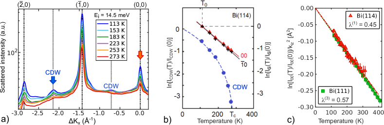
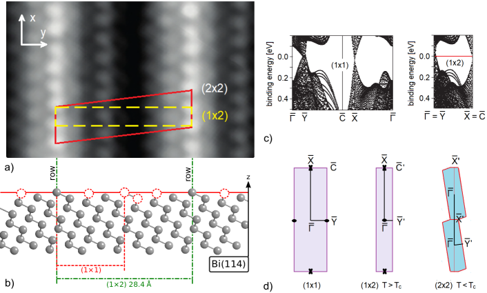
As a good 1DEG example, it is shown that a CDW diffraction peak also may be used to extract away from the critical region. The ideal (114) truncation of bismuth (footnote †) is characterized by parallel atomic rows along the direction, separated by Å in the normal direction , with a unit cell including two rows ( Å) and one atom per row (atom spacing along the rows Å). At room temperature, the Bi(114) surface is reconstructed in a fashion with 3 missing rows out of 4, so as to have one row per unit cell ( Å) and one atom per row [footnote †a) and b)]. The electronic structure, calculated by Wells et al.26 for the phase [footnote †c), left], shows cones centered at the and points [footnote †c) and d)] at the Fermi level. Those at are folded into in the reconstructed phase. Both electronic structures allow for a multivalley CDW via e-ph interaction, the former with a 2D character, the latter with a pure 1D character due to the cone alignment along with a spacing. HAS angular distributions along 13 [Figure 2a)] show the growth of additional peaks at and below K, indicating the formation of a surface commensurate CDW.13 The associated reconstruction consists of a dimerisation along the rows. The portion of the Bi(114)- STM image reproduced in footnote †b) from Hofmann et al.32, 13 suggests a phase correlation between rows, giving an oblique () unit cell and a corresponding elongated hexagonal Brillouin zone (BZ) [footnote †d)].
The HAS DW exponents for the specular , diffraction , and CDW peaks measured as a function of temperature below are plotted in Figure 2b). The specular and diffraction DW exponents have almost the same slopes, the small difference being compensated by the ratio , resulting in the same values of within less than 1%. The input data in Eq. (2) for are eV33, Å-1, Å, incident energy meV, and fixed scattering angle of , so Å-2. The diffraction occurs at the incident angle of , which gives Å-2, and the resulting e-ph coupling constant is , being the same value for both specular and diffractive channels.
The CDW peak intensity, Figure 2b), shows the expected critical behavior with , so that a value of can only be estimated from the slope at the lowest temperatures. This is smaller than that for the specular peak by and is compensated for approximately the same amount by the correcting factor , the incident angle for the CDW peak at being . Thus it is reasonable to conclude that consistent values of can be extracted from the -dependence of the CDW peaks.
It is interesting to compare the value for Bi(114) to that previously derived for Bi(111), either treated as a 3D system where 10, in agreement with the value of in Hofmann’s review32, or as a 2D system with (a single bilayer) where it is found that ,12 in fair agreement with a recent ab-initio calculation by Ortigoza et al. for Bi(111)34 which yielded , just as found here for Bi(114). As seen in Figure 2c), the DW exponent has about the same slope for Bi(111) and Bi(114), when it is divided by , in order to account for the different incident energy used in HAS experiments. The fact that [Bi(114)] [Bi(111)] reflects the dimensionality effect of , in the prefactor of Eq. (2). Incidentally, we note that treating Bi(114) as a 2D system would yield a five times smaller, probably unphysical, value for due to the large surface unit cell area.
Layered chalcogenides, such as 2D topological materials, with strong intralayer and weak interlayer forces form a wide class of quasi-2D materials with a conducting surface. Some transition-metal dichalcogenides (TMDC) have been investigated with HAS since the late eighties in connection with CDW transitions, related Kohn anomalies in the bulk, and surface phonon dispersion curves.35, 36, 37, 38, 39, 40 More recently, HAS studies have been extended to the surface of other TMDCs like 2H-MoS2(0001) 41 and 1T-PtTe2 42, as well as to pnictogen chalcogenides with surface topological electronic bands at the Fermi level, like Bi2Te3 43, 14, 44, Bi2Se3 45, 15, etc. The 2D expression for the e-ph coupling constant in Eq. (3) is the one to be used for these systems. When dealing with the e-ph coupling constant expressed as an average over the whole phonon spectrum and over all electronic transitions across the Fermi level, natural questions are: a) which phonons contribute most, and b) which electronic states at the Fermi level are more important.
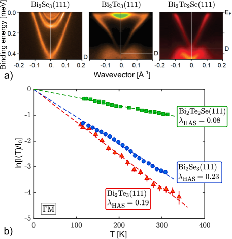
The theoretical analysis by Heid et al. 49 of the mode-selected e-ph coupling constants shows that in pnictogen chalcogenides, optical phonons give the major contribution to e-ph interaction, and therefore to the DW exponent. Both Bi2Se3(111)15 and Bi2Te3(111)44 exhibit two highly dispersed optical branches with deep minima at for 3rd-layer longitudinal polarization and at for (mostly) 3rd-layer shear-vertical (SV3) polarisation. Their optical character and largest amplitude at the central chalcogen layer of the quintuple layer endow these modes with a dipolar character and therefore a large e-ph interaction, consistent with the Heid et al. theoretical analysis 49. Spin-echo 3He scattering data from Bi2Te3(111) 44 suggest a Kohn anomaly also in the longitudinal acoustic branch corresponding to a nesting across the Dirac cone above the surface conduction-band minimum. As discussed in 49, the interband e-ph coupling occurring when the Fermi level is above the surface conduction-band minimum is enhanced largely by the involvement of surface quantum-well states. This conclusion is confirmed by the following analysis of in Bi chalcogenides as a function of the Fermi level position.
The temperature dependence of HAS reflectivity from the three Bi chalcogenide surfaces Bi2Se3(111), Bi2Te3(111), and Bi2Te3-xSex(111) (phase II with 59,‡‡‡‡‡‡According to the surface lattice constant as determined by HAS and Fig. 1(b) of 59, for the present sample., hereafter approximated by Bi2Te2Se(111)) has been measured for three samples whose surface electronic states near the Fermi level, in particular the topological Dirac states and the quantum-well states above the surface conduction-band minimum, are known from angle-resolved photoemission spectroscopy (ARPES) data 52, 46, 47, 48. As seen in footnote †† (top panel), the binding energy of the Dirac point (D) with respect to the Fermi energy decreases in the sequence Bi2Se3(111), Bi2Te3(111), Bi2Te2Se(111), as does the surface conduction-band minimum (from eV, to eV and , respectively). Correspondingly, the DW exponent slope derived from the HAS specular intensity as a function of temperature also decreases. Similar behavior is expected for the e-ph coupling constant , which is shown in Table 1. The latter is derived from Eq. (3) by setting , where is the quintuple layer (QL) thickness and is the Thomas-Fermi screening length, accounting for the surface band-bending extension in degenerate semiconductors and semimetals 60. The factor 2 in the above expression of accounts for the fact that each QL contains two metal (Bi) layers. Note that the Fermi-level density of states includes the factor 2 for spin multiplicity, and this is appropriate for the quantum-well states above the surface conduction-band minimum that mostly contribute to . On the other hand, no factor of 2 in is necessary when only the Dirac states are involved, due to their multiplicity of 1. The uncertainties () given for in the following are based on the confidence bounds of the DW slope. Other sources in terms of the uncertainty are , and with the largest contribution likely to be due to . Taken together it is safe to assume a relative uncertainty of about 10% for as shown in Table 1.
With the input data collected in Table 1 and the DW exponent slopes displayed in footnote †† (bottom panel), it is found that for Bi2Se3(111), for Bi2Te3(111), and for Bi2Te2Se(111), in good agreement with selected results from other sources (Table 1, last column). This clearly indicates the dominant role of surface quantum well (QW) states over the modest contribution of Dirac electrons. The enhancement effect of QW states and related interband transitions has been investigated thoroughly by Chen et al. 50 with high resolution ARPES for the family Bi2Te3-xSex(111) , including n-type Bi2Te3(111), and theoretically for Bi2Se3(111) and Bi2Te3(111) by Heid et al. 49. As shown by Pan et al. 61, in accurate ARPES studies on bulk Bi2Se3(111) samples, where only Dirac topological states are involved because the Fermi level is less than 0.3 eV above the Dirac point, the e-ph coupling constant turns out to be quite small, ranging from to , similar to that found with HAS in Bi2Te2Se(111) under similar conditions.
Since the surface QW states extend into the bulk on the order of , i.e., much longer than the penetration of surface Dirac states, it is interesting to compare the above results for with the corresponding values of when these materials are treated as 3D materials. The ratio , with [footnote †† (top)] and representing the 3DEG thickness, turns out to be .
Unlike Bi(114), where the quasi-1D character of the electron gas is quite evident, in layered pnictogen chalcogenides the considerable penetration of the QW states gives . This is consistent with the fact that the QW states are the surface states which provide the major contribution to the e-ph interaction. Information about which phonons contribute most to can also be obtained from inelastic HAS intensities, as explained in the introduction. The Kohn anomalies reported in the lower part of the phonon spectrum 43, 44, 45 are indicative of a strong e-ph coupling for specific wavevectors and frequencies, though it has been predicted that the major contribution in these materials comes from polar optical modes49. Indeed this is in agreement with recent HAS measurements of the phonon dispersion curves in Bi2Se3(111)15, which indicate the longitudinal optical branch L3 (with the largest displacement on the 3rd (Se) atomic plane) as the one having the largest mode-selective e-ph coupling.
In conclusion, it has been shown that the temperature dependence of HAS reflectivity allows for the determination of the electron-phonon coupling constant of topological semimetal surfaces. In the case of the quasi-1D Bi(114) surface, the DW factor from the CDW diffraction peak yields an e-ph coupling constant consistent with that derived from the reflectivity. Therefore the e-ph interaction acts as the driving mechanism for the observed multi-valley CDW transition. In the absence of spin-orbit coupling, the phonon angular momentum cannot convert into an electron spin-flip, so no good nesting would be allowed across the Dirac cone, and only the strong spin-orbit coupling occurring in topological materials allows for a comparatively weak e-ph intra-cone interaction. The multi-valley mechanism at the zone boundary overcomes the nesting problem, because with more Dirac cones separated by less than a G vector, there is always a good inter-cone (i.e., multi-valley) nesting, even for opposite chiralities. Such a favorable circumstance, allowing for a substantial in Bi(114) and a CDW transition, does not occur in pnictogen chalcogenides, due to the single Dirac cone location at the center of the BZ. Most of their appreciable e-ph interaction is provided by the QW states, as long as they are located at the Fermi level. The present extension of HAS -analysis from metal surfaces 9, 10 and thin metal films 11 to topological semimetal surfaces qualifies He atom scattering as a universal tool for the measurement of electron-phonon coupling in conducting low-dimensional systems.
1 Experimental Methods
The experimental data of this work was obtained at the HAS apparatus in Graz62 and the 3He spin-echo scattering apparatus in Cambridge19. In both cases the scattered intensity of a nearly monochromatic He beam in the range of meV is monitored as a function of incident angle and at various surface temperatures. The DW measurement of Bi2Te3 can be found in 14 while the DW data of Bi2Se3 is reported in Ref. 15. Most of the Bi(114) data has been published in the work of Hofmann et al.13, whereas the Bi2Te2Se experimental data is presented here for the first time.
2 Acknowledgements
One of us (G.B.) would like to thank Profs. M. Bernasconi (Milano-Bicocca) and E. V. Chulkov and P. M. Echenique (DIPC, San Sebastian) for many helpful discussions. This work is partially supported by a grant with Ref. FIS2017-83473-C2-1-P from the Ministerio de Ciencia Universidades e Innovación (Spain). A.R., W.E.E. and A.T. acknowledge financial support provided by the FWF (Austrian Science Fund) within the projects J3479-N20 and P29641-N36. G. B. gratefully acknowledges the Italian Ministry of University and Research (MIUR) for financial support through grant “Dipartimenti di Eccellenza - 2017 Materials for Energy”. We would like to thank Martin Bremholm, Ellen M. J. Hedegaard, and Bo B. Iversen for the synthesis of the samples, Marco Bianchi for his advice and help in terms of the sample preparation, and Philip Hofmann as well as the aforementioned people for many helpful discussions and additional characterizations of the samples.
References
- Saito et al. 2017 Saito, Y.; Nojima, T.; Iwasa, Y. Highly crystalline 2D superconductors. Nat. Rev. Mater 2017, 2, 16094
- Zhang and Melo 2018 Zhang, W.; Melo, C. A. R. S. D. In Quasi-One-Dimensional Organic Superconductors; Zhang, W., Ed.; Advanced Physics Series; World Scientific, 2018; Vol. 5
- Liang et al. 2016 Liang, J.; Cheng, L.; Zhang, J.; Liu, H.; Zhang, Z. Maximizing the thermoelectric performance of topological insulator Bi2Te3 films in the few-quintuple layer regime. Nanoscale 2016, 8, 8855–8862
- Dolinšek et al. 2009 Dolinšek, J.; Smontara, A.; Barišić, O. S.; Gille, P. Phonon-enhanced thermoelectric power of Y-Al-Ni-Co decagonal approximant. Z. Kristallogr. 2009, 224, 64
- McMillan 1968 McMillan, W. L. Transition Temperature of Strong-Coupled Superconductors. Phys. Rev 1968, 167, 331
- Grimvall 1981 Grimvall, G. The Electron-Phonon Interaction in Metals; North-Holland: New York, 1981
- Allen 1972 Allen, P. B. Neutron Spectroscopy of Superconductors. Phys. Rev. B 1972, 6, 2577
- Sklyadneva et al. 2011 Sklyadneva, I. Y.; Benedek, G.; Chulkov, E. V.; Echenique, P. M.; Heid, R.; Bohnen, K.-P.; Toennies, J. P. Mode-Selected Electron-Phonon Coupling in Superconducting Pb Nanofilms Determined from He Atom Scattering. Phys. Rev. Lett. 2011, 107, 095502
- Benedek et al. 2014 Benedek, G.; Bernasconi, M.; Bohnen, K.-P.; Campi, D.; Chulkov, E. V.; Echenique, P. M.; Heid, R.; Sklyadneva, I. Y.; Toennies, J. P. Unveiling mode-selected electron-phonon interactions in metal films by helium atom scattering. Phys. Chem. Chem. Phys 2014, 16, 7159
- Manson et al. 2016 Manson, J. R.; Benedek, G.; Miret-Artés, S. Electron-phonon coupling strength at metal surfaces directly determined from the helium atom scattering Debye-Waller factor. J. Phys. Chem. Lett. 2016, 7, 1016
- Benedek et al. 2018 Benedek, G.; Miret-Artés, S., S.; Toennies, J. P.; Manson, J. R. The Electron–Phonon Coupling Constant of Metallic Overlayers from Specular He Atom Scattering. J. Phys. Chem. Lett. 2018, 9, 76–83
- Manson et al. unpublished Manson, J. R.; Benedek, G.; Miret-Artés, S. Atom scattering as a probe of the surface electron-phonon interaction. Surf. Sci. Rep. unpublished,
- Hofmann et al. 2019 Hofmann, P.; Ugeda, M. M.; Tamtögl, A.; Ruckhofer, A.; Ernst, W. E.; Benedek, G.; Martínez-Galera, A. J.; Stróżecka, A.; Gómez-Rodríguez, J. M.; Rienks, E. et al. Strong-coupling charge density wave in a one-dimensional topological metal. Phys. Rev. B 2019, 99, 035438
- Tamtögl et al. 2017 Tamtögl, A.; Kraus, P.; Avidor, N.; Bremholm, M.; Hedegaard, E. M. J.; Iversen, B. B.; Bianchi, M.; Hofmann, P.; Ellis, J.; Allison, W. et al. Electron-Phonon Coupling and Surface Debye Temperature of Bi2Te3(111) from Helium Atom Scattering. Phys. Rev. B 2017, 95, 195401
- Ruckhofer et al. 2020 Ruckhofer, A.; Campi, D.; Bremholm, M.; Hofmann, P.; Benedek, G.; Bernasconi, M.; Ernst, W. E.; Tamtögl, A. THz Surface Modes and Electron-Phonon Coupling in Bi2Se3(111). Phys. Rev. Res. 2020, in review, preprint, https://arxiv.org/abs/1907.01864
- Manson et al. 2016 Manson, J. R.; Benedek, G.; Miret-Artés, S. Correction to “Electron-Phonon Coupling Strength at Metal Surfaces Directly Determined from the Helium Atom Scattering Debye-Waller Factor”. J. Phys. Chem. Lett. 2016, 7, 1691–1691
- Coxeter 1969 Coxeter, H. S. M. Introduction to Geometry, second edition ed.; John Wiley and Sons: New York, 1969
- Beeby 1971 Beeby, J. L. Scattering of Helium Atoms from Surfaces. J. Physics C 1971, 4, L359
- Jardine et al. 2009 Jardine, A.; Hedgeland, H.; Alexandrowicz, G.; Allison, W.; Ellis, J. Helium-3 spin-echo: principles and application to dynamics at surfaces. Prog. Surf. Sci. 2009, 84, 323–379
- Peierls 1955 Peierls, R. E. Quantum theory of solids; Oxford Univ. Press: Oxford, 1955
- Fröhlich 1954 Fröhlich, H. On the Theory of Superconductivity: The One-Dimensional Case. Proc. R. Soc. Lond 1954, 223, 296
- Kelly and Falicov 1977 Kelly, M. J.; Falicov, L. M. Electronic Ground-State of Inversion Layers in Many-Valley Semiconductors. Phys. Rev. B 1977, 15, 1974
- Kelly and Falicov 1977 Kelly, M. J.; Falicov, L. M. Optical-Properties of Charge-Density-Wave ground-States for Inversion Layers in Many-Valley Semiconductors. Phys. Rev. B 1977, 15, 1983
- Kelly and Falicov 1976 Kelly, M. J.; Falicov, L. M. Electronic Structure of Inversion Layers in Many-Valley Semiconductors. Phys. Rev. Lett. 1976, 37, 1021
- Tamtögl et al. 2019 Tamtögl, A.; Kraus, P.; Mayrhofer-Reinhartshuber, M.; Benedek, G.; Bernasconi, M.; Dragoni, D.; Campi, D.; Ernst, W. E. Statics and Dynamics of Multivalley Charge Density Waves in Sb(111). npj Quantum Mater. 2019, 4, 18
- Wells et al. 2009 Wells, J. W.; Dil, J. H.; Meier, F.; Lobo-Checa, J.; Petrov, V. N.; Osterwalder, J.; Ugeda, M. M.; Fernandez-Torrente, I.; Pascual, J. I.; Rienks, E. D. L. et al. Nondegenerate Metallic States on Bi(114): A One-Dimensional Topological Metal. Phys. Rev. Lett. 2009, 102, 096802
- Liu et al. 2019 Liu, R.; Ma, T.; Wang, S.; Yang, J. Thermodynamical Potentials of Classical and Quantum Systems. Discrete and Continuous Dynamical Systems-Series B 2019, 24, 1411
- Ma and Wang 2009 Ma, T.; Wang, S. Cahn-Hilliard Equations and Phase Transition Dynamics for Binary Systems. Discrete and Continuous Dynamical Systems B 2009, 11, 741
- Ge and Liu 2013 Ge, Y.; Liu, A. Y. Phonon-mediated superconductivity in electron-doped single-layer MoS2: A first-principles prediction. Phys. Rev. B 2013, 87, 241408
- Liu 2009 Liu, A. Y. Electron-phonon coupling in compressed 1T-TaS2: Stability and superconductivity from first principles. Phys. Rev. B 2009, 79, 220515
- Benedek et al. 1994 Benedek, G.; Hofmann, F.; Ruggerone, P.; Onida, G.; Miglio, L. Surface Phonons in Layered Crystals - Theoretical Aspects. Surf. Sci. Rep. 1994, 20, 3
- Hofmann 2006 Hofmann, P. The surfaces of bismuth: Structural and electronic properties. Prog. Surf. Sci. 2006, 81, 191
- Michaelson 1977 Michaelson, H. B. The work function of the elements and its periodicity. J. Appl. Phys. 1977, 48, 4729
- Ortigoza et al. 2014 Ortigoza, M. A.; Sklyadneva, I. Y.; Heid, R.; Chulkov, E. V.; Rahman, T. S.; Bohnen, K.-P.; Echenique, P. M. Ab initio lattice dynamics and electron-phonon coupling of Bi(111). Phys. Rev. B 2014, 90, 195438
- Benedek et al. 1987 Benedek, G.; Miglio, L.; Skofronick, J. G.; Brusdeylins, G.; Heimlich, C.; Toennies, J. P. Surface Phonon Dynamics in 2H-TaSe2(001). J. Vac. Sci Technol. A 1987, 5, 1093
- Benedek et al. 1988 Benedek, G.; Brusdeylins, G.; Heimlich, C.; Miglio, L.; Skofronick, J.; Toennies, J. P. Shifted Surface Phonon Anomaly in 2H-TaSe2(001). Phys. Rev. Lett. 1988, 60, 1037
- Brusdeylins et al. 1989 Brusdeylins, G.; Heimlich, C.; Skofronick, J. G.; Toennies, J. P.; Vollmer, R.; Benedek, G. Determination of the Critical Exponents for a Charge Density Wave Transition in 2H-TaSe2 by Helium Atom Scattering. Euro Phys Lett 1989, 9, 563
- Brusdeylins et al. 1990 Brusdeylins, G.; Hofmann, F.; Toennies, J. P.; Vollmer, R.; Benedek, G.; Ruggerone, P.; Skofronick, J. In Phonons; S. Hunklinger, W. L., Weiss, G., Eds.; World Sci.: Singapore, 1990; p 892
- Benedek et al. 1992 Benedek, G.; Miglio, L.; Seriani, G. In Helium Atom Scattering from Surfaces; Hulpke, E., Ed.; Springer: Heidelberg, 1992; pp 207–242
- Benedek et al. 1994 Benedek, G.; Brusdeylins, G.; Hofmann, F.; Ruggerone, P.; Toennies, J.; Vollmer, R.; Skofronick, J. Strong coupling of Rayleigh phonons to charge density waves in 1T-TaS2. Surf. Sci. 1994, 304, 185 – 190
- Anemone et al. 2019 Anemone, G.; Taleb, A. A.; Benedek, G.; Castellanos-Gomez, A.; Farías, D. Electron-Phonon Coupling Constant of 2H-MoS2(0001) from Helium-Atom Scattering. J. Phys. Chem. C 2019, 123, 3682–3686
- Anemone et al. 2020 Anemone, G.; Garnica, M.; Zappia, M.; Aguilar, P. C.; Taleb, A. A.; Kuo, C.-N.; Lue, C. S.; Politano, A.; Benedek, G.; de Parga, A. L. V. et al. Experimental determination of surface thermal expansion and electron-phonon coupling constant of 1T-PtTe2. 2D Mater. 2020, 7, 025007
- Howard et al. 2013 Howard, C.; El-Batanouny, M.; Sankar, R.; Chou, F. C. Anomalous behavior in the phonon dispersion of the (001) surface of Bi2Te3 determined from helium atom-surface scattering measurements. Phys. Rev. B 2013, 88, 035402
- Tamtögl et al. 2018 Tamtögl, A.; Campi, D.; Bremholm, M.; Hedegaard, E. M. J.; Iversen, B. B.; Bianchi, M.; Hofmann, P.; Marzari, N.; Benedek, G.; Ellis, J. et al. Nanoscale surface dynamics of Bi2Te3(111): observation of a prominent surface acoustic wave and the role of van der Waals interactions. Nanoscale 2018, 10, 14627–14636
- Zhu et al. 2011 Zhu, X.; Santos, L.; Sankar, R.; Chikara, S.; Howard, C. .; Chou, F. C.; Chamon, C.; El-Batanouny, M. Interaction of Phonons and Dirac Fermions on the Surface of : A Strong Kohn Anomaly. Phys. Rev. Lett. 2011, 107, 186102
- Bianchi et al. 2012 Bianchi, M.; Hatch, R. C.; Guan, D.; Planke, T.; Mi, J.; Iversen, B. B.; Hofmann, P. The electronic structure of clean and adsorbate-covered Bi2Se3: an angle-resolved photoemission study. Semicond. Sci. Technol. 2012, 27, 124001
- Michiardi et al. 2014 Michiardi, M.; Aguilera, I.; Bianchi, M.; de Carvalho, V. E.; Ladeira, L. O.; Teixeira, N. G.; Soares, E. A.; Friedrich, C.; Blügel, S.; Hofmann, P. Bulk band structure of . Phys. Rev. B 2014, 90, 075105
- Barreto et al. 2014 Barreto, L.; Kühnemund, L.; Edler, F.; Tegenkamp, C.; Mi, J.; Bremholm, M.; Iversen, B. B.; Frydendahl, C.; Bianchi, M.; Hofmann, P. Surface-Dominated Transport on a Bulk Topological Insulator. Nano Lett. 2014, 14, 3755–3760
- Heid et al. 2017 Heid, R.; Sklyadneva, I. Y.; Chulkov, E. V. Electron-phonon coupling in topological surface states: The role of polar optical modes. Sci. Rep. 2017, 7, 1095
- Chen et al. 2013 Chen, C.; Xie, Z.; Feng, Y.; Yi, H.; Liang, A.; He, S.; Mou, D.; He, J.; Peng, Y.; Liu, X. et al. Tunable Dirac fermion dynamics in topological insulators. Sci. Rep. 2013, 3, 2411
- Suh et al. 2014 Suh, J.; Fu, D.; Liu, X.; Furdyna, J. K.; Yu, K. M.; Walukiewicz, W.; Wu, J. Fermi-level stabilization in the topological insulators Bi2Se3 and Bi2Te3: Origin of the surface electron gas. Phys. Rev. B 2014, 89, 115307
- Bianchi et al. 2010 Bianchi, M.; Guan, D.; Bao, S.; Mi, J.; Iversen, B. B.; King, P. D.; Hofmann, P. Coexistence of the topological state and a two-dimensional electron gas on the surface of Bi2Se3. Nat. Commun. 2010, 1, 128
- Ruckhofer et al. 2019 Ruckhofer, A.; Tamtögl, A.; Pusterhofer, M.; Bremholm, M.; Ernst, W. E. Helium-Surface Interaction and Electronic Corrugation of Bi2Se3(111). J. Phys. Chem. C 2019, 123, 17829–17841
- Hatch et al. 2011 Hatch, R. C.; Bianchi, M.; Guan, D.; Bao, S.; Mi, J.; Iversen, B. B.; Nilsson, L.; Hornekær, L.; Hofmann, P. Stability of the (111) topological state: Electron-phonon and electron-defect scattering. Phys. Rev. B 2011, 83, 241303
- Zeljkovic et al. 2015 Zeljkovic, I.; Scipioni, K. L.; Walkup, D.; Okada, Y.; Zhou, W.; Sankar, R.; Chang, G.; Wang, Y. J.; Lin, H.; Bansil, A. et al. Nanoscale determination of the mass enhancement factor in the lightly doped bulk insulator lead selenide. Nat. Commun. 2015, 6, 6559–
- Pettes et al. 2013 Pettes, M. T.; Maassen, J.; Jo, I.; Lundstrom, M. S.; Shi, L. Effects of Surface Band Bending and Scattering on Thermoelectric Transport in Suspended Bismuth Telluride Nanoplates. Nano Lett. 2013, 13, 5316
- Tamtögl et al. 2018 Tamtögl, A.; Pusterhofer, M.; Bremholm, M.; Hedegaard, E. M.; Iversen, B. B.; Hofmann, P.; Ellis, J.; Allison, W.; Miret-Artés, S.; Ernst, W. E. A Helium-Surface Interaction Potential of Bi2Te3(111) from Ultrahigh-Resolution Spin-Echo Measurements. Surf. Sci. 2018, 678, 25–31
- Gehring et al. 2012 Gehring, P.; Gao, B. F.; Burghard, M.; Kern, K. Growth of High-Mobility Bi2Te2Se Nanoplatelets on hBN Sheets by van der Waals Epitaxy. Nano Lett. 2012, 12, 5137
- Mi et al. 2013 Mi, J.-L.; Bremholm, M.; Bianchi, M.; Borup, K.; Johnsen, S.; Søndergaard, M.; Guan, D.; Hatch, R. C.; Hofmann, P.; Iversen, B. B. Phase Separation and Bulk p-n Transition in Single Crystals of Bi2Te2Se Topological Insulator. Adv. Mater 2013, 25, 889–893
- Shklovskii and Efros 1984 Shklovskii, B. I.; Efros, A. E. Electronic Properties of Doped Semiconductors; Springer, 1984
- Pan et al. 2012 Pan, Z.-H.; Fedorov, A. V.; Gardner, D.; Lee, Y. S.; Chu, S.; Valla, T. Measurement of an Exceptionally Weak Electron-Phonon Coupling on the Surface of the Topological Insulator Using Angle-Resolved Photoemission Spectroscopy. Phys. Rev. Lett. 2012, 108, 187001
- Tamtögl et al. 2010 Tamtögl, A.; Mayrhofer-Reinhartshuber, M.; Balak, N.; Ernst, W. E.; Rieder, K. H. Elastic and inelastic scattering of He atoms from Bi(111). J. Phys. Condens. Matter 2010, 22, 304019