Low power switching of magnetization using enhanced magnetic anisotropy with short-voltage-pulse application
Abstract
A low power magnetization switching scheme based on the voltage control of magnetic anisotropy (VCMA) is proposed. In contrast to the conventional switching scheme using VCMA, where the magnetic anisotropy is eliminated during the voltage pulse, the magnetic anisotropy is enhanced to induce precession around the axis close to the easy axis. After turning off the voltage proximately at a half of precession period, the magnetization relaxes to the opposite equilibrium direction. We perform numerical simulations and show that the pulse duration of the proposed switching scheme is as short as a few tens of pico seconds. Such a short pulse duration is beneficial for low power consumption because of the reduction of energy loss by Joule heating.
I Introduction
Low power consumption is a key requirement for modern computational devices. Non-volatility is one of the core concepts to reduce power consumption for logics and memories in normally-off computing Ando (2001); Ando et al. (2014); Nakada and Nakamura (2017). Magnetoresistive random access memory (MRAM) is a promising non-volatile memory that stores information associated with the direction of magnetization in magnetic tunnel junctions (MTJs) Yuasa et al. (2004); Parkin et al. (2004); Djayaprawira et al. (2005); Yuasa and Djayaprawira (2007); Kishi et al. (2008); Kitagawa et al. (2012); Apalkov et al. (2016); Sbiaa and Piramanayagam (2017); Cai et al. (2017). In order to reduce power consumption of MRAM, several types of writing schemes have been developed. The currently used writing scheme is based on the spin-transfer-torque (STT) switching phenomena, which were proposed by Slonczewski Slonczewski (1989, 1996) and independently by Berger Berger (1996). The write energy of STT-MRAM is of the order of 100 fJ/bit Kitagawa et al. (2012); Cai et al. (2017), which is still 2 orders of magnitude larger than that of static random-access memory.
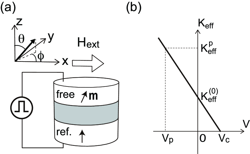
Discovery of the voltage control of magnetic anisotropy (VCMA) effect Weisheit et al. (2007); Maruyama et al. (2009); Duan et al. (2008); Nakamura et al. (2009); Tsujikawa and Oda (2009); Nozaki et al. (2010); Endo et al. (2010); Nozaki et al. (2014); Skowroński et al. (2015); Nozaki et al. (2016); Li et al. (2017) paved the way for further reduction of write energy in MRAM. The mechanism of VCMA in an MgO-based MTJ is considered to be the combination of the selective electron or hole doping into the -electron orbitals and the induction of a magnetic dipole moment, which affect the electron spin through spin-orbit interaction Duan et al. (2008); Nakamura et al. (2009); Tsujikawa and Oda (2009); Miwa et al. (2017). The MRAM which uses the VCMA effect to switch magnetization is called the voltage controlled MRAM (VC-MRAM) Shiota et al. (2012a, b); Kanai et al. (2012); Shiota et al. (2016); Grezes et al. (2016); Kanai et al. (2016); Shiota et al. (2017); Matsumoto et al. (2018); Yamamoto et al. (2018, 2019); Matsumoto et al. (2019); Imamura and Matsumoto (2019); Matsumoto and Imamura (2019). The writing procedure of a conventional VC-MRAM is as follows. The perpendicularly magnetized MTJ is subjected to an in-plane external magnetic field () as shown in Fig. 1(a). The magnetic anisotropy (MA) constant of the free layer can be controlled by applying voltage () as shown in Fig. 1(b). Here, is the effective perpendicular anisotropy constant where the demagnetization energy is subtracted from the perpendicular anisotropy constant. Throughout the paper, the superscript (0) indicates the quantities at . The voltage pulse with critical amplitude eliminates the MA and induces the precession of the magnetization around the external magnetic field. By turning off the voltage at one half period of precession, the magnetization switching completes.
The write energy of VC-MRAM is estimated from the Joule heating energy loss during the pulse. Assuming that the voltage pulse with amplitude and duration is applied to the MTJ with resistance , the write energy is given by
| (1) |
To reduce the write energy, the VC-MRAM should be designed to have large resistance and short pulse duration. The pulse duration is given by a half period of precession as
| (2) |
where is the Gilbert damping constant and is the gyromagnetic ratio. For example, = 0.18 ns for = 0.1 and = 100 mT, where is the vacuum permeability. Recently, Grezes . demonstrated a very small write energy of 6 fJ/bit for the VC-MRAM with k at = 1.96 V and = 0.52 ns Grezes et al. (2016). The similar results were also obtained independently by Kanai . Kanai et al. (2016).
It is difficult to use MTJ with huge to further reduce write energy because the read time of the VC-MRAM increases with increase of . Adopting a scheme of decreasing pulse duration by increasing external magnetic field should also be avoided since the application of a strong in-plane magnetic field deteriorates the thermal stability factor defined as
| (3) |
where is the Boltzmann constant, is the temperature, is the saturation magnetization, and is the volume of the free layer.
In this paper, we propose another switching scheme which could reduce the pulse duration and therefore the write energy of a VC-MRAM. The main difference between the conventional scheme and the proposed switching scheme is the polarity of the voltage pulse. Application of the voltage pulse with the polarity that is opposite to the conventional switching can enhance the magnetic anisotropy and induce the precession around the axis close to the easy axis. After turning off the voltage proximately at a half of precession period, the magnetization relaxes to the opposite equilibrium direction and the switching completes. We perform numerical simulations and demonstrate that the pulse duration of the proposed switching scheme is as short as a few tens of pico seconds. We also evaluate the write error rate (WER) and show that the WER is minimized if the pulse duration is about half the period of precession similar to the conventional switching scheme.
II Theoretical model
The system we consider is schematically shown in Fig. 1(a). The macrospin model is employed to describe the magnetization dynamics. The direction of the magnetization in the free layer is represented by the unit vector , , , , ), where and are the polar and azimuthal angles. The axis is parallel to the direction of external in-plane magnetic field .
The energy density of the free layer is given by
| (4) |
The first term of Eq. (4) is the sum of the shape, the bulk crystalline and the interfacial anisotropies. Owing to the VCMA effect, can be controlled by application of as shown in Fig. 1(b). Here represents the effective anisotropy constant without the voltage application. We assume that decreases with increase of and vanishes at . Applying the voltage increases to and induces the precessional motion of around the effective magnetic field. The effective field is given by , where is the anisotropy field.
The magnetization dynamics is simulated by solving the following Landau-Lifshitz-Gilbert equation Brown (1963),
| (5) |
where represents the thermal agitation field satisfying the following relations:
| (6) | |||
| (7) |
Here , and denotes the statistical average of .
Throughout this paper, we assume that the external field is = 100 mT and the saturation magnetization of the free layer is kA/m. Also the radius of the junction area is assumed as nm and the thickness of the free layer, nm, and therefore the volume of the free layer as nm3. The initial states are prepared by 10 ns relaxation from the equilibrium direction at , that is Matsumoto et al. (2019). The write error rates are calculated from trials with 10 ns relaxation after the pulse.
III Results and discussions
First we show the difference between the mechanisms of the conventional voltage controlled switching and the proposed switching that utilizes the enhancement of the magnetic anisotropy. This can be accomplished by analyzing the switching trajectories at . Figures 2(a) and (b) show the shape of the voltage pulse and the corresponding time dependence of the effective anisotropy constant for the conventional voltage controlled switching. The induced switching dynamics of at is shown in Figs. 2(c) together with the color map of the energy density of Eq. (4) at . Thin black dotted curves represent energy contours. Thick black curves represent the energy contour crossing . The initial direction of the magnetization is the equilibrium direction with indicated by the black circle, which we call as the “up state”.
In Figs. 2(a), (b) and (c), application of the voltage pulse with eliminates the magnetic anisotropy and induce the precession of around the external magnetic field as represented by the red curve. After turning off the voltage at one-half period of precession, the magnetization starts to relax from the point indicated by the orange circle to the other equilibrium direction with , i. e. the “down state”, indicated by the black circle. Note that the black circle at is illustrated under the green curve. The switching is thus completed as represented by the green curve.
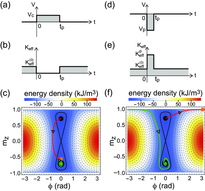
Figures 2(d) and (e) show the shape of the voltage pulse and the corresponding time dependence of the effective anisotropy constant for the switching using the enhanced . The induced switching dynamics of at is shown in Fig. 2(f) together with the color map of the energy density at = 0. The initial state is the up state indicated by the black circle at . Application of the voltage pulse with enhances the effective anisotropy constant from to and induce the precession of around the effective magnetic field as represented by the red curve. The value of is assumed to be 400 kJ/m3, which gives the anisotropy field of = 570 mT. The effective field is nearly parallel to the easy axis or the axis because the directional cosine of the effective field relative to the easy axis is 0.98. The voltage is turned off at about a half period of the precession, and the magnetization reaches the point, indicated by the orange circle. As will be shown later, the write error rate (WER) is minimized if the pulse duration is set about half the period of precession. After turning off the pulse, the magnetization relaxes to the down state and completes the switching as shown by the green curve. The proposed switching scheme does not reduce the thermal stability factor of Eq. (3) because it just enhances during the voltage pulse.
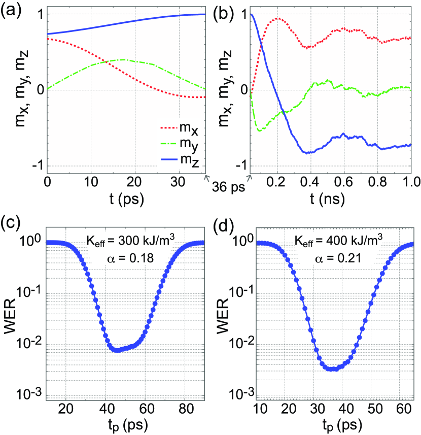
Next we discuss the switching properties of the proposed switching scheme at = 300 K by analyzing the numerical simulations results. The time evolution of the Cartesian components of for a typical switching trajectory during the pulse are shown in Fig. 3(a). The value of kJ/m3 and are the same as in Fig. 2(f), = 400 kJ/m3 and = 0.21. During the pulse duration, increases with the increase of time because the effective anisotropy constant is enhanced. The shapes of and are very similar to the cosine and sine functions, respectively, because precesses around the effective field which is almost parallel to the axis. Figure 3(b) shows the time evolution of , and after the pulse. Please note that the horizontal axis is in unit of ns. monotonically decreases with the increase of time and the switching completes at around 0.4 ns.
Figures 3(c) and (d) show the pulse duration, , dependence of the write error rate (WER) for different values of and . The parameters are = 300 kJ /m3 and = 0.18 for Fig. 3(c), and = 400 kJ /m3 and = 0.21 for Fig. 3(d). In Fig. 3(c), the WER takes a minimum value of at = 46 ps. In Fig. 3(d), the WER takes a minimum value of at = 36 ps. These optimal values of at which the WER is minimized are almost the same as one half period of precession around .
IV conclusion
In summary, we propose a low power switching scheme of magnetization using enhanced magnetic anisotropy by applying a short voltage pulse. The proposed switching scheme can reduce the pulse duration and therefore the write energy substantially without deteriorating thermal stability. We perform numerical simulations and show that the pulse duration of the proposed switching scheme is as short as a few tens of pico seconds. We also calculated the pulse duration dependence of the WER, and showed that the optimal values of at which the WER is minimized are nearly half the period of precession around the effective field.
Acknowledgements.
This work was partly supported by JSPS KAKENHI Grant No. JP19K05259 and 19H01108.References
- Ando (2001) K. Ando, “Nonvolatile magnetic memory,” FED J. [in Japanese] 12, 89–95 (2001).
- Ando et al. (2014) K. Ando, S. Fujita, J. Ito, S. Yuasa, Y. Suzuki, Y. Nakatani, T. Miyazaki, and H. Yoda, “Spin-transfer torque magnetoresistive random-access memory technologies for normally off computing (invited),” J. Appl. Phys. 115, 172607 (2014).
- Nakada and Nakamura (2017) Takashi Nakada and Hiroshi Nakamura, eds., Normally-Off Computing (Springer Japan, Tokyo, 2017).
- Yuasa et al. (2004) Shinji Yuasa, Taro Nagahama, Akio Fukushima, Yoshishige Suzuki, and Koji Ando, “Giant room-temperature magnetoresistance in single-crystal Fe/MgO/Fe magnetic tunnel junctions,” Nat. Mater. 3, 868–871 (2004).
- Parkin et al. (2004) Stuart S. P. Parkin, Christian Kaiser, Alex Panchula, Philip M. Rice, Brian Hughes, Mahesh Samant, and See-Hun Yang, “Giant tunnelling magnetoresistance at room temperature with MgO (100) tunnel barriers,” Nat. Mater. 3, 862–867 (2004).
- Djayaprawira et al. (2005) David D. Djayaprawira, Koji Tsunekawa, Motonobu Nagai, Hiroki Maehara, Shinji Yamagata, Naoki Watanabe, Shinji Yuasa, Yoshishige Suzuki, and Koji Ando, “230% room-temperature magnetoresistance in CoFeB/MgO/CoFeB magnetic tunnel junctions,” Appl. Phys. Lett. 86, 092502 (2005).
- Yuasa and Djayaprawira (2007) S. Yuasa and D. D. Djayaprawira, “Giant tunnel magnetoresistance in magnetic tunnel junctions with a crystalline MgO(0 0 1) barrier,” J. Phys. D: Appl. Phys. 40, R337 (2007).
- Kishi et al. (2008) T. Kishi, H. Yoda, T. Kai, T. Nagase, E. Kitagawa, M. Yoshikawa, K. Nishiyama, T. Daibou, M. Nagamine, M. Amano, S. Takahashi, M. Nakayama, N. Shimomura, H. Aikawa, S. Ikegawa, S. Yuasa, K. Yakushiji, H. Kubota, A. Fukushima, M. Oogane, T. Miyazaki, and K. Ando, “Lower-current and fast switching of a perpendicular TMR for high speed and high density spin-transfer-torque MRAM,” in IEDM Tech. Dig. 12.6 (2008).
- Kitagawa et al. (2012) E. Kitagawa, S. Fujita, K. Nomura, H. Noguchi, K. Abe, K. Ikegami, T. Daibou, Y. Kato, C. Kamata, S. Kashiwada, N. Shimomura, J. Ito, and H. Yoda, “Impact of ultra low power and fast write operation of advanced perpendicular MTJ on power reduction for high-performance mobile CPU,” in IEDM Tech. Dig. (2012) pp. 29.4.1–29.4.4.
- Apalkov et al. (2016) Dmytro Apalkov, Bernard Dieny, and J. M. Slaughter, “Magnetoresistive random access memory,” Proceedings of the IEEE 104, 1796–1830 (2016).
- Sbiaa and Piramanayagam (2017) Rachid Sbiaa and S. N. Piramanayagam, “Recent developments in spin transfer torque MRAM,” physica status solidi (RRL) Rapid Research Letters 11, 1700163 (2017).
- Cai et al. (2017) Hao Cai, Wang Kang, You Wang, Lirida Alves De Barros Naviner, Jun Yang, and Weisheng Zhao, “High performance MRAM with spin-transfer-torque and voltage-controlled magnetic anisotropy effects,” Applied Sciences 7, 929 (2017).
- Slonczewski (1989) J. C. Slonczewski, “Conductance and exchange coupling of two ferromagnets separated by a tunneling barrier,” Phys. Rev. B 39, 6995–7002 (1989).
- Slonczewski (1996) J. C. Slonczewski, “Current-driven excitation of magnetic multilayers,” J. Magn. Magn. Mater. 159, L1–L7 (1996).
- Berger (1996) L. Berger, “Emission of spin waves by a magnetic multilayer traversed by a current,” Phys. Rev. B 54, 9353–9358 (1996).
- Weisheit et al. (2007) Martin Weisheit, Sebastian Fhler, Alain Marty, Yves Souche, Christiane Poinsignon, and Dominique Givord, “Electric field-induced modification of magnetism in thin-film ferromagnets,” Science 315, 349–351 (2007).
- Maruyama et al. (2009) T. Maruyama, Y. Shiota, T. Nozaki, K. Ohta, N. Toda, M. Mizuguchi, A. A. Tulapurkar, T. Shinjo, M. Shiraishi, S. Mizukami, Y. Ando, and Y. Suzuki, “Large voltage-induced magnetic anisotropy change in a few atomic layers of iron,” Nat. Nano. 4, 158–161 (2009).
- Duan et al. (2008) Chun-Gang Duan, Julian P. Velev, R. F. Sabirianov, Ziqiang Zhu, Junhao Chu, S. S. Jaswal, and E. Y. Tsymbal, “Surface magnetoelectric effect in ferromagnetic metal films,” Phys. Rev. Lett. 101, 137201 (2008).
- Nakamura et al. (2009) Kohji Nakamura, Riki Shimabukuro, Yuji Fujiwara, Toru Akiyama, Tomonori Ito, and A. J. Freeman, “Giant modification of the magnetocrystalline anisotropy in transition-metal monolayers by an external electric field,” Phys. Rev. Lett. 102, 187201 (2009).
- Tsujikawa and Oda (2009) Masahito Tsujikawa and Tatsuki Oda, “Finite electric field effects in the large perpendicular magnetic anisotropy surface Pt/Fe/Pt(001): A first-principles study,” Phys. Rev. Lett. 102, 247203 (2009).
- Nozaki et al. (2010) T. Nozaki, Y. Shiota, M. Shiraishi, T. Shinjo, and Y. Suzuki, “Voltage-induced perpendicular magnetic anisotropy change in magnetic tunnel junctions,” Appl. Phys. Lett. 96, 022506 (2010).
- Endo et al. (2010) M. Endo, S. Kanai, S. Ikeda, F. Matsukura, and H. Ohno, “Electric-field effects on thickness dependent magnetic anisotropy of sputtered MgO/Co40Fe40B20/Ta structures,” Appl. Phys. Lett. 96, 212503 (2010).
- Nozaki et al. (2014) Takayuki Nozaki, Hiroko Arai, Kay Yakushiji, Shingo Tamaru, Hitoshi Kubota, Hiroshi Imamura, Akio Fukushima, and Shinji Yuasa, “Magnetization switching assisted by high-frequency-voltage-induced ferromagnetic resonance,” Appl. Phys. Express 7, 073002 (2014).
- Skowroński et al. (2015) Witold Skowroński, Takayuki Nozaki, Yoichi Shiota, Shingo Tamaru, Yakushiji Kay, Hitoshi Kubota, Akio Fukushima, Shinji Yuasa, and Yoshishige Suzuki, “Perpendicular magnetic anisotropy of Ir/CoFeB/MgO trilayer system tuned by electric fields,” Appl. Phys. Express 8, 053003 (2015).
- Nozaki et al. (2016) Takayuki Nozaki, Anna Kozioł-Rachwał, Witold Skowroński, Vadym Zayets, Yoichi Shiota, Shingo Tamaru, Hitoshi Kubota, Akio Fukushima, Shinji Yuasa, and Yoshishige Suzuki, “Large voltage-induced changes in the perpendicular magnetic anisotropy of an MgO-based tunnel junction with an ultrathin Fe layer,” Phys. Rev. Applied 5, 044006 (2016).
- Li et al. (2017) Xiang Li, Kevin Fitzell, Di Wu, C. Ty Karaba, Abraham Buditama, Guoqiang Yu, Kin L. Wong, Nicholas Altieri, Cecile Grezes, Nicholas Kioussis, Sarah Tolbert, Zongzhi Zhang, Jane P. Chang, Pedram Khalili Amiri, and Kang L. Wang, “Enhancement of voltage-controlled magnetic anisotropy through precise control of Mg insertion thickness at CoFeB|MgO interface,” Appl. Phys. Lett. 110, 052401 (2017).
- Miwa et al. (2017) Shinji Miwa, Motohiro Suzuki, Masahito Tsujikawa, Kensho Matsuda, Takayuki Nozaki, Kazuhito Tanaka, Takuya Tsukahara, Kohei Nawaoka, Minori Goto, Yoshinori Kotani, Tadakatsu Ohkubo, Frédéric Bonell, Eiiti Tamura, Kazuhiro Hono, Tetsuya Nakamura, Masafumi Shirai, Shinji Yuasa, and Yoshishige Suzuki, “Voltage controlled interfacial magnetism through platinum orbits,” Nature Communications 8, 15848 (2017).
- Shiota et al. (2012a) Yoichi Shiota, Takayuki Nozaki, Frédéric Bonell, Shinichi Murakami, Teruya Shinjo, and Yoshishige Suzuki, “Induction of coherent magnetization switching in a few atomic layers of FeCo using voltage pulses,” Nat. Mater. 11, 39–43 (2012a).
- Shiota et al. (2012b) Yoichi Shiota, Shinji Miwa, Takayuki Nozaki, Frédéric Bonell, Norikazu Mizuochi, Teruya Shinjo, Hitoshi Kubota, Shinji Yuasa, and Yoshishige Suzuki, “Pulse voltage-induced dynamic magnetization switching in magnetic tunneling junctions with high resistance-area product,” Appl. Phys. Lett. 101, 102406 (2012b).
- Kanai et al. (2012) S. Kanai, M. Yamanouchi, S. Ikeda, Y. Nakatani, F. Matsukura, and H. Ohno, “Electric field-induced magnetization reversal in a perpendicular-anisotropy CoFeB-MgO magnetic tunnel junction,” Appl. Phys. Lett. 101, 122403 (2012).
- Shiota et al. (2016) Yoichi Shiota, Takayuki Nozaki, Shingo Tamaru, Kay Yakushiji, Hitoshi Kubota, Akio Fukushima, Shinji Yuasa, and Yoshishige Suzuki, “Evaluation of write error rate for voltage-driven dynamic magnetization switching in magnetic tunnel junctions with perpendicular magnetization,” Appl. Phys. Express 9, 013001 (2016).
- Grezes et al. (2016) C. Grezes, F. Ebrahimi, J. G. Alzate, X. Cai, J. A. Katine, J. Langer, B. Ocker, P. Khalili Amiri, and K. L. Wang, “Ultra-low switching energy and scaling in electric-field-controlled nanoscale magnetic tunnel junctions with high resistance-area product,” Appl. Phys. Lett. 108, 012403 (2016).
- Kanai et al. (2016) S. Kanai, F. Matsukura, and H. Ohno, “Electric-field-induced magnetization switching in CoFeB/MgO magnetic tunnel junctions with high junction resistance,” Appl. Phys. Lett. 108, 192406 (2016).
- Shiota et al. (2017) Yoichi Shiota, Takayuki Nozaki, Shingo Tamaru, Kay Yakushiji, Hitoshi Kubota, Akio Fukushima, Shinji Yuasa, and Yoshishige Suzuki, “Reduction in write error rate of voltage-driven dynamic magnetization switching by improving thermal stability factor,” Appl. Phys. Lett. 111, 022408 (2017).
- Matsumoto et al. (2018) R. Matsumoto, T. Nozaki, S. Yuasa, and H. Imamura, “Voltage-induced precessional switching at zero-bias magnetic field in a conically magnetized free layer,” Phys. Rev. Applied 9, 014026 (2018).
- Yamamoto et al. (2018) Tatsuya Yamamoto, Takayuki Nozaki, Yoichi Shiota, Hiroshi Imamura, Shingo Tamaru, Kay Yakushiji, Hitoshi Kubota, Akio Fukushima, Yoshishige Suzuki, and Shinji Yuasa, “Thermally induced precession-orbit transition of magnetization in voltage-driven magnetization switching,” Phys. Rev. Applied 10, 024004 (2018).
- Yamamoto et al. (2019) Tatsuya Yamamoto, Takayuki Nozaki, Hiroshi Imamura, Yoichi Shiota, Takuro Ikeura, Shingo Tamaru, Kay Yakushiji, Hitoshi Kubota, Akio Fukushima, Yoshishige Suzuki, and Shinji Yuasa, “Write-error reduction of voltage-torque-driven magnetization switching by a controlled voltage pulse,” Phys. Rev. Applied 11, 014013 (2019).
- Matsumoto et al. (2019) Rie Matsumoto, Tomoyuki Sato, and Hiroshi Imamura, “Voltage-induced switching with long tolerance of voltage-pulse duration in a perpendicularly magnetized free layer,” Appl. Phys. Express 12, 053003 (2019).
- Imamura and Matsumoto (2019) Hiroshi Imamura and Rie Matsumoto, “Impact of spin-transfer torque on the write-error rate of a voltage-torque-based magnetoresistive random-access memory,” Phys. Rev. Applied 11, 064019 (2019).
- Matsumoto and Imamura (2019) R. Matsumoto and H. Imamura, “Methods for reducing write error rate in voltage-induced switching having prolonged tolerance of voltage-pulse duration,” AIP Advances 9, 125123 (2019).
- Brown (1963) William Fuller Brown, “Thermal fluctuations of a single-domain particle,” Phys. Rev. 130, 1677–1686 (1963).