Controlling the dopant profile for SRH suppression at low current densities
in 1330nm GaInAsP light-emitting diodes
Abstract
The quantum efficiency of double hetero-junction light-emitting diodes (LEDs) can be significantly enhanced at low current density by tailoring the spatial profile of dopants to suppress Shockley-Read-Hall (SRH) recombination. To demonstrate this effect we model, design, grow, fabricate, and test a GaInAsP LED ( 1330nm) with an unconventional dopant profile. Compared against that of our control design, which is a conventional -- double hetero-junction LED, the dopant profile near the - hetero-structure of the new design displaces the built-in electric field in such a way as to suppress the space charge recombination current. The design principle generalizes to other material systems and could be applicable to efforts to observe and exploit electro-luminescent refrigeration at practical power densities.
As the solar photovoltaic and solid-state lighting industries have continued to deliver reductions in both the cost per semiconductor area and cost per Watt of their energy technology products Trube et al. (2019); Haitz et al. (2000); Steele (2007); Haitz and Tsao (2011); Gerke, Ngo, and Fisseha (2015), the technology platforms which share capital base with them have become serious contenders for scalable new energy technologies. Two of the most durable sources of demand for energy conversion which have yet to be “semiconductorized” are air conditioning and waste heat recovery. Both of these demands have potentially viable solutions utilizing III-V opto-electronicsXiao et al. (2019); Heikkila, Oksanen, and Tulkki (2009); Piprek and Li (2016); Chen et al. (2017); Harder and Green (2003); Zhao et al. (2018). However it is also true that high-efficiency realizations of opto-electronic devices that can in theory meet these needs often carry the same stringent requirements on quantum efficiency as do Light-Emitting Diodes (LEDs) utilizing electro-luminescent cooling to act as refrigerators.
As a result, despite multiple recent demonstrations of photonic heat flux control capable of solid state coolingHehlen et al. (2018); Zhu et al. (2019); Radevici et al. (2019), the pace of progress on these potential new energy technologies has been limited by the technical challenges of fabricating devices with high enough quantum efficiencies for cooling at practical power densities. The general problem is two-fold: first electron-hole pairs injected into the luminescing material must be efficiently converted into photons within that material, and second the photons thus generated must be able to escape the high refractive index typical of the luminescent materials which allow the first point to be satisfied.
Serious progress in overcoming both of these challenges has been made experimentally in the past few years Radevici et al. (2019); Kuritzky et al. (2017); Li et al. (2019). The light extraction efficiency challenge has been addressed in at least two distinct ways. First, a recent experiment redesigned LED structures Kuritzky et al. (2017) in the well-developed blue Nitride LED material system for low current density where thinner current-spreading layers which significantly reduce the probability that recycled photons will be lost to irreversible absorption in contact metal can be sufficient. Second, but no less relevant, GaAs photo-diodes that served as photon-absorbing detectors were grown in series with GaAs emitters in the same epitaxial layer stack thereby enabling direct light extraction from the LED to the photodetector, which is more efficient as compared with light extraction from an LED to free spaceRadevici et al. (2019).
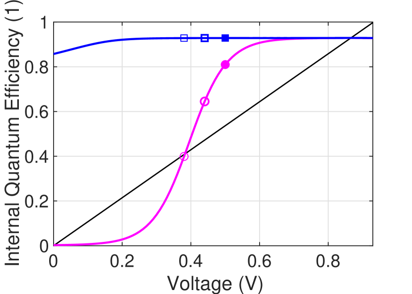
The other half of the technical challenge, to increase the fraction of injected electron-hole pairs which recombine radiatively (i.e. the Internal Quantum Efficiency or IQE to the light-emitter community; alternatively the Internal Radiative Efficiency or IRE to the photo-voltaic community), has recently been approached by attempts to suppress parasitic SRH recombination that prevents cooling from being observed at lower forward bias voltages, where the problem of light extraction is more forgiving. Operating an LED at a slightly lower forward bias voltage than typical results in a larger ratio between the so-called photon voltage , where is the emitted photon’s energy and is the charge of an electron, and the applied voltage . When the ratio is greater than unity but by a small margin, as tends to be the case in blue Nitride LEDs (even at current densities considered low relative to most practical devices), the margin for error is correspondingly small. A ratio of , for instance, implies that no more than 3% of the internally generated photons may be lost to parasitic absorbing structures (e.g. contacts) without entirely eliminating the possibility of net cooling. A ratio of , however, increases this margin for error ten-fold, making experimental realization drastically more tractable. While this approach does sacrifice power density, it makes observation of a large steady-state temperature reduction of the emitting device less demanding and could enable photonic solid state coolers that support large temperature differences with very small cold-side heat loads in the near future.
Recent work has produced a near-infrared LED with suppressed SRH recombination at the values of most relevant to electro-luminescent coolingLi et al. (2019). In Ref. Li et al., 2019, the authors designed, fabricated, and tested an LED which made use of the spectacularly low interfacial surface recombination velocity at the hetero-interface between the luminescent material (1.3eV-GaInAs) and the wider bandgap carrier confining material (GaInP) to extend the high IQE of near-infrared LEDs to much lower current densities where non-radiative Shockley-Read-Hall recombination is usually dominant. The structure in Ref. Li et al., 2019 utilizes a very thin GaInAs quantum well to confine the injected carriers to a narrow interval in the growth direction where they experience non-radiative Shockley-Read-Hall (SRH) recombination a very small fraction of the time. Thus they observe very high IQE from their LEDs even at forward biases 200 mV below the emitted photon energy. This strategy for increased IQE, however, comes at the price of current density as only electron-hole pairs in this same narrow interval can contribute to radiative recombination. As a result, the current density achieved in Ref. Li et al., 2019 is more than two orders of magnitude below the detailed-balance limit for an opaque body of the same bandgap. In pursuit of applications with more moderate current densities, such as most cooling experiments to date, some of this may be addressed by the use of multiple quantum wells or much thicker emitting layers but whether such structures can retain high IQE performance remains to be seen.
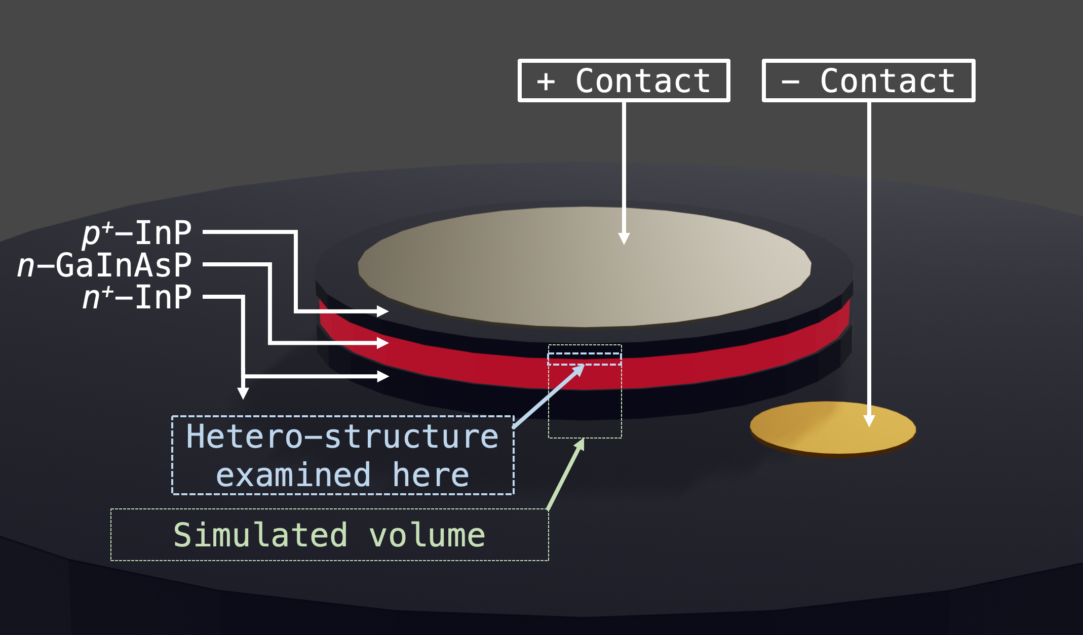
In this work we aimed to improve IQE at deep-sub-bandgap bias voltages through a distinct SRH suppression strategy, alluded to but not fully examined in Ref. Gray Jr., Santhanam, and Ram, 2013, which utilizes a micron-thick emitting layer so that even in a device realization with near-complete SRH suppression, the diode remains near the detailed balance limit for current density. We report work on GaInAsP LEDs, grown lattice-matched to their InP substrates and emitting photons at a free-space wavelength of 1330nm, whose epitaxial layer stack design aims to extend downward the range of forward bias voltages where high IQE is observed by the suppression of bulk non-radiative SRH recombination. We subsequently fabricate devices resembling Fig. 1(a) and characterize them. Our approach targets the bulk SRH recombination in the electrically non-neutral space charge region around the - junction (i.e. the often-parasitic current Grove (1967) contribution that causes the - curve to exhibit a diode ideality factor of 2) of a conventional near-infrared LED with a micron-scale emitting layer. It does so in a way that is readily generalized to other promising material systems including GaAs.
By inserting one higher-doped layer into the -GaInAsP and one lower-doped layer into the -InP regions directly surrounding the - junction, the spatial distribution of bulk SRH can theoretically be displaced enough to place its peak in the wider bandgap material. As we show presently, the aggregate rate at which carriers undergo SRH recombination integrated over the volume of the device is thereby reduced by orders of magnitude.
Design. The epitaxial layer stack designs on which the experimental results of this Letter are based are shown in Table 1 with the layers modified to achieve SRH suppression highlighted. Design includes the proposed suppression layers while Design serves as a control against which to evaluate Design .
|
Material |
|
|
||||||
| 480 | -InP | 1 | 1 | ||||||
| 20 | -InP | 1 | 1 | ||||||
| 20 | -GaInAsP | 2.26 | 4 | ||||||
| 980 | -GaInAsP | 4 | 4 | ||||||
| 50 | -InP | 4 | 4 | ||||||
| 1250 | -InP | 2 | 2 | ||||||
| 200 | -InP | 1 | 1 | ||||||
| 370m | -InP | Semi-Insulating | Semi-Insulating |
To explain the design process and clarify the intended generalizations of the design principle into other material systems, we focus on the electron transport in the region surrounding the - hetero-junction buried 500 nm below the surface in each design (i.e. where the two designs differ). We seek to model the transport in this region in the case of a forward bias voltage that is below the band gap energy’s voltage scale by several multiples of the thermal voltage (, where is Boltzmann’s constant, is the absolute temperature of the semiconductor lattice, and is the magnitude of the electron’s charge). This voltage regime has been previously referred toSanthanam (2015) as the “deep sub-bandgap” bias regime and is tens to hundreds of milli-volts below the bias voltages where LEDs are typically designed to operate. At these deep sub-bandgap operating points, a very significant fraction of the current which flows through the device corresponds to leakage through trap-assisted SRH recombination.
Furthermore, the standard formulation of SRH recombination indicates that the spatial distribution of SRH recombination is highly localized around a particular plane normal to the growth direction. In this Letter, we refer to this plane as the Active Trap plane and denote its position as . Here we have used the standard formulationHall (1952); Shockley and Read Jr. (1952); Grove (1967) for the local rate of trap-assisted Shockley-Read-Hall (SRH) recombination as expressed in the following equation:
| (1) |
The above equation assumes the trap spectrum is a delta function and nonzero only at the intrinsic Fermi level of each semiconductor. If we further assume that the SRH lifetimes of the electrons and holes are equal (i.e. ), we may further simplify the denominator of Equation 1 to find that
| (2) |
Since and are varying in and away from the hetero-junction itself that variation is monotonic, if we temporarily assume the removed parts of Equation 1 are not varying spatially, we should expect a local maximum to around the plane where is minimized. Since in quasi-equilibrium, the product of the electron and hole concentrations is fixed for a fixed Fermi level separation, this minimum is located where =. This defines : has a local maximum at .
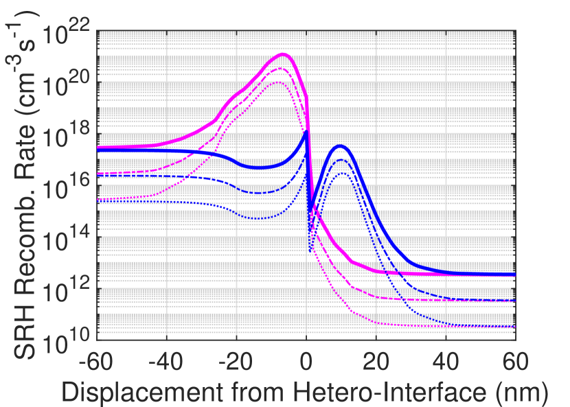
Fig. 1(b) depicts the results of numerical simulations conducted with the commercial electron transport CHARGE solver within Lumerical DeviceLumerical, Inc. . We find that the net recombination rate per unit volume near for Designs and side-by-side. Design (i.e. blue curves) has its peak 10 nanometers away from the hetero-interface into the wide-bandgap -InP. Design (i.e. magenta curves) has its peak 7 nanometers away from the hetero-interface into the narrower-bandgap -GaInAsP.
Due to the strength of the built-in electric field in this region and our assumptions about the trap spectrum, this local maximum is fairly sharp. For operating points in the deep sub-bandgap bias regime, a field strength of order 107 V/m is typical. In this case we may use the room temperature rule of thumb of 60 meV/decade for the exponential decay of the concentration of electrons and holes as a function of voltage in the Boltzmann limit at 300 K to quantify this sharpness. For the assumed field strength, a plane corresponding to just 6 nanometers away from would have either or a full ten times the value of . Since both and enter the denominator additively in Equation (2), this indicates that 99% of the integrated recombination takes place within a 25 nm window around . For the admittedly unphysical case of a perfect delta function trap spectrum, this corresponds to more than half of the recombination being localized within a window of width 50 Å.
Temporarily neglecting the additional complication of the hetero-junction, the physical interpretation of this peak is reasonably simple. Outside of this window, we find the traps are less active. If we consider planes displaced in the growth direction toward the terminal of the device, we find that the hole concentration is too low there and so the SRH process is bottlenecked by slow hole capture rates. Similarly, in planes displaced in the growth direction toward the terminal of the device, we find that the electron concentration is too low and the SRH process is bottlenecked by slow electron capture rates.
For our control structure in Design , this peak falls within the narrow bandgap GaInAsP active region. Our goal in Design is to displace this spatial peak in SRH rate into the wider gap InP material so that the term in the numerator of Equation (1) can suppress it. To do this we will modify the dopant impurity profile from that in Design to that in Design as shown in Table 1.
Fabrication. Custom epitaxial growths were purchased commercially from OEpic, Inc. in Sunnyvale, CA. Growth was done by MOCVD on Fe-doped semi-insulating InP substrates. The growths reported here were all done during a pair of back-to-back runs of the same reactor with the intention of eventually comparing device characteristics in a controlled manner.
The first set of experiments done to verify that the films had been grown as intended were Photo-Luminescence (PL) measurements on the bare epitaxy. The PL spectra at room temperatures are shown later on the right vertical axis of subfigure (b) in Fig. 3. Cryogenic PL measurements were also done on samples which had undergone a mesa etch but no further processing. The cryogenic measurements were taken in a chamber cooled by liquid helium but due to imperfect heat sinking in the sample mounting solution, the exact temperature of the sample was highly uncertain. The primary conclusion of the PL experiments was that the devices fabricated from this epitaxy should emit light with a free space wavelength of around 1330nm.
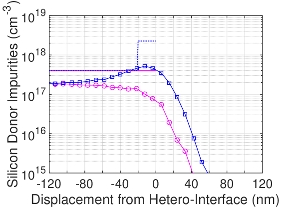
The second set of experiments was aimed at verifying the distinction between the films grown to meet the two different design specifications. Secondary Ion Mass Spectrometry (SIMS) analysis was done commercially by Evans Analytical Group. The primary conclusion drawn from the SIMS data shown in Fig. 2 was that the intended silicon donor concentration in the emitting-bandgap SRH suppression layer was significantly higher than in the corresponding layer of the control sample, but was far enough short of the design to create a much smaller change in the IQE of resulting LEDs than is suggested by Fig. 1(c). As shown in Fig. 2, the additional silicon donors detected by SIMS were localized to a volume 60 nm thick in the growth direction rather than the 20 nm in the design. Moreover the -integrated density of silicon donors in the sample grown targeting Design exceeded that of the sample grown targeting Design by 1.81012 cm-2 as compared against an excess donor density of 3.71012 cm-2 anticipated based on the designs. Unfortunately neither the actual concentrations of free carriers nor the ionization fraction of the silicon dopants has yet been measured directly in any part of the epitaxial films.
Next, diodes were fabricated from these films. We utilized the photo-lithography capabilities of the tools managed by the Stanford Nanofabrication Facility and the Stanford Nano Shared Facilities, with particular reliance on the Heidelberg Maskless Aligner MLA150, Shipley S1813 photo-resist, and Metal-Free developer MF319. All masks were designed manually with Python scripts used to generate CIF files. Etching was done by a combination of 3:1 H3PO4:HCl, which selectively etched the InP, and 1:1:10 H2O:H2O2:H2SO4, which selectively etched the GaInAsP quaternary. The contacts were formed by lift-off processes utilizing the same resists as for the etch masks and a pair of deposition tools. The -type contacts were simple Ti/Pt/Au films deposited using electron beam evaporation. The -type contacts were annealed Pd/Zn/Pd. Prior to the -metal contacts reported here, a generation of devices was made using simple Ti/Pt/Au for both contact types and, due to the absence of a epitaxial contact layer, the resulting Schottky barriers prohibited meaningful - and - characterization.
Two types of diode structures were fabricated and tested. Small circular mesa type diodes with an active emitting area of 0.1 mm2 each were designed for high current density. Larger square mesa diodes were designed for lower current density measurements, each having an active emitting area of 8 mm2.
Characterization. Finally the characteristic Current-Voltage (i.e. -) and Light-Current (i.e. -) behaviors of the devices were measured. Imperfections in various stages of the fabrication process led to some variation in device behavior both within a given die and from die-to-die. Particularly common were parasitic shunt pathways presumed to arise from flashes of contact metal unintentionally attached to the surface of the devices amid the lift-off contact fabrication process.
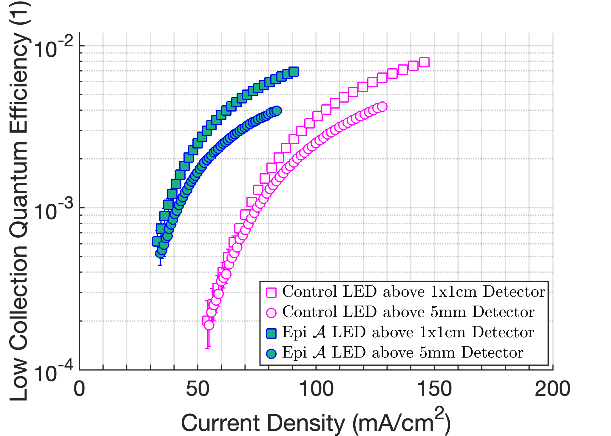
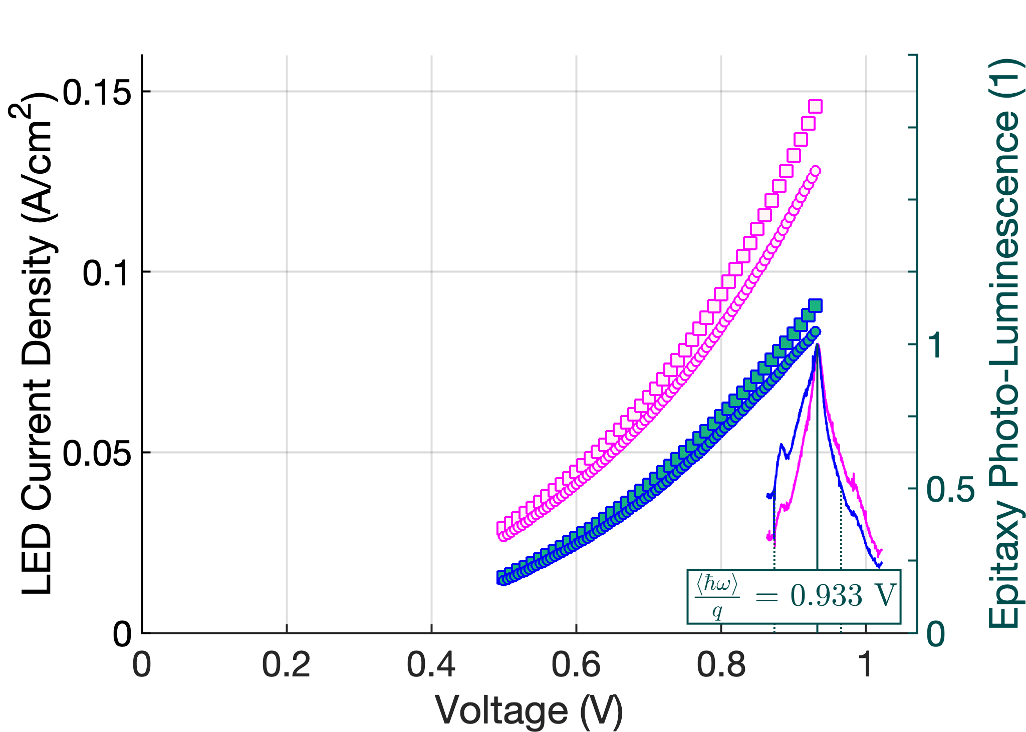
Experiments were performed primarily near room temperature, measured at about 295 K. The fabricated diodes were placed in a variety of geometries near a 1 cm2 ThorLabs FDG10X10 large-area free-space Germanium photo-diode as well as a smaller ThorLabs FDG05 Germanium photo-diode of 5 mm diameter. These photo-current from these detectors was then amplified by a ThorLabs PDA200C TIA to measure the electro-luminescence signal. Configurations in which the substrate of the LED suffered from limited repeatability which we ascribe to dust and other debris, a hypothesis supported by significant increases in the signal seen when high-index immersion oil was used at the interface. For the sake of maximal repeatability, the measurements we present here were taken when the emitting diode chips were placed atop a nylon washer at a height about 1 mm above the photo-sensitive surface of each of the two detectors described above. The devices were probed in a manual probe station with shielded electrical connections to a Keithley 2635B Sourcemeter.
Figure 3 presents data taken on the large 8 mm2 diodes. It indicates that the epitaxial layer stack design change from Design to Design resulted in less current leaking through the device in the deep sub-bandgap bias regime as intended. The measurements are compatible with a moderate suppression of non-radiative recombination at low current densities, leading to improved quantum efficiency at these operating points.
Conclusions. The series of experiments reported here provides significant evidence that a rational design of the dopant profile of a near-infrared LED represents a viable technical de-risking trajectory for the development of novel energy conversion devices based on the net refrigeration of an LED at bias voltages .
Acknowledgements.
Dr. Ping-Show Wong of OEpic performed the MOCVD epitaxial growth. Room temperature PL spectra were acquired in collaboration with Dr. Tomás Sarmiento in the lab of Prof. Jelena Vuckovic. Tom Carver deposited the -metal Ti/Pt/Au. Dr. Michelle Sherrott helped diagnose an early -metal issue. Prof. Eric Pop provided advice and aid in characterization facilities access. The selective wet etch recipes were based on suggestions from Dr. Vijay Jayaraman of Praevium Research, Inc. This work was supported by the US Department of Energy “Light-Material Interactions in Energy Conversion” Energy Frontier Research Center under grant no. DE-SC0001293 and the US Department of Energy “Photonics at Thermodynamic Limits” Energy Frontier Research Center under grant no. DE-SC0019140.References
- Trube et al. (2019) J. Trube, M. Fischer, G. Erfert, C.-C. Li, P. Ni, M. Woodhouse, P. Li, A. Metz, I. Saha, R. Chen, and Q. Wang, “International technology roadmap for photovoltaic (ITRPV),” Industry sponsored report (Steering committee of the ITRPV, 2019) 10th Edition.
- Haitz et al. (2000) R. Haitz, F. Kish, J. Tsao, and J. Nelson, “The case for a national research program on semiconductor lighting,” Sandia Report SAND2000-1612 (Sandia National Laboratories, Sandia National Laboratories, Albuquerque, New Mexico 87185 and Livermore, California 94550, 2000).
- Steele (2007) R. V. Steele, “The story of a new light source,” Nature Photonics 1 (2007), 10.1038/nphoton.2006.44, Market Analysis: Technology Focus.
- Haitz and Tsao (2011) R. Haitz and J. Y. Tsao, “Solid-state lighting: ‘The case’ 10 years after and future prospects,” Phys. Status Solidi A 208, 17–29 (2011).
- Gerke, Ngo, and Fisseha (2015) B. F. Gerke, A. T. Ngo, and K. S. Fisseha, “Recent price trends and learning curves for household led lamps from a regression analysis of internet retail data,” DOE Office of Energy Efficiency and Renewable Energy (EERE) report LBNL-184075 (US Department of Energy, Lawrence Berkeley National Laboratory, Environmental Energy Technologies Division, 2015).
- Xiao et al. (2019) T. P. Xiao, K. Chen, P. Santhanam, S. Fan, and E. Yablonovitch, “Practical efficiency limits of electroluminescent cooling,” Proc. SPIE 10936: Photonic Heat Engines: Science and Applications (2019), 10.1117/12.2509231.
- Heikkila, Oksanen, and Tulkki (2009) O. Heikkila, J. Oksanen, and J. Tulkki, “Ultimate limit and temperature dependency of light-emitting diode efficiency,” Journal of Applied Physics 105 (2009), 10.1063/1.3125514.
- Piprek and Li (2016) J. Piprek and Z.-M. Li, “Electroluminescent cooling mechanism in ingan/gan light-emitting diodes,” Optical and Quantum Electronics 48 (2016), 10.1007/s11082-016-0729-1.
- Chen et al. (2017) K. Chen, T. P. Xiao, P. Santhanam, E. Yablonovitch, and S. Fan, “High-performance near-field electroluminescent refrigeration device consisting of a gaas light emitting diode and a si photovoltaic cell,” Journal of Applied Physics 122 (2017), 10.1063/1.5007712.
- Harder and Green (2003) N.-P. Harder and M. A. Green, “Thermophotonics,” Semiconductor Science and Technology (2003), 10.1088/0268-1242/18/5/319.
- Zhao et al. (2018) B. Zhao, P. Santhanam, K. Chen, S. Buddhiraju, and S. Fan, “Near-field thermophotonic systems for low-grade waste-heat recovery,” Nano Letters 18, 5224–5230 (2018).
- Hehlen et al. (2018) M. P. Hehlen, J. Meng, A. R. Albrecht, E. R. Lee, A. Gragossian, S. P. Love, C. E. Hamilton, R. I. Epstein, and M. Sheik-Bahae, “First demonstration of an all-solid-state optical cryocooler,” Light: Science & Applications 7 (2018), 10.1038/s41377-018-0028-7.
- Zhu et al. (2019) L. Zhu, A. Fiorino, D. Thompson, R. Mittapally, E. Meyhofer, and P. Reddy, “Near-field photonic cooling through control of the chemical potential of photons,” Nature 566, 239–244 (2019).
- Radevici et al. (2019) I. Radevici, J. Tiira, T. Sadi, S. Ranta, A. Tukiainen, M. Guina, and J. Oksanen, “Thermophotonic cooling in GaAs based light emitters,” Applied Physics Letters 114 (2019), 10.1063/1.5064786.
- Kuritzky et al. (2017) L. Y. Kuritzky, A. C. Espenlaub, B. P. Yonkee, C. D. Pynn, S. P. DenBaars, S. Nakamura, C. Weisbuch, and J. S. Speck, “High wall-plug efficiency blue III-Nitride leds designed for low current density operation,” Optics Express 25 (2017), 10.1364/OE.25.030696.
- Li et al. (2019) N. Li, K. Han, W. Spratt, S. Bedell, J. Ott, M. Hopstaken, F. Libsch, Q. Li, and D. Sadana, “Ultra-low-power sub-photon-voltage high-efficiency light emitting diodes,” Nature Photonics 13, 588–592 (2019).
- Gray Jr., Santhanam, and Ram (2013) D. J. Gray Jr., P. Santhanam, and R. J. Ram, “Design for thermo-electric pumping in light emitting diodes,” Applied Physics Letters 103 (2013), 10.1063/1.4821266.
- Grove (1967) A. S. Grove, Physics and technology of semiconductor devices (John Wiley & Sons, Inc., 1967) library of Congress Catalog Card Number 67-17340.
- Santhanam (2015) P. Santhanam, “Electro-luminescent cooling in the deep sub-bandgap bias regime,” Proc. SPIE 9000: Laser Refrigeration of Solids VII (2015), 10.1117/12.2040497.
- Hall (1952) R. N. Hall, “Electron-hole recombination in germanium,” Physical Review 87 (1952), 10.1103/PhysRev.87.387.
- Shockley and Read Jr. (1952) W. Shockley and W. T. Read Jr., “Statistics of the recombinations of holes and electrons,” Physical Review 87, 835–842 (1952).
- (22) Lumerical, Inc., “https://www.lumerical.com/products/,” .