Topological Photonic Tamm-States and the Su-Schrieffer-Heeger Model
Abstract
In this paper we study the formation of topological Tamm states at the interface between a semi-infinite one-dimensional photonic-crystal and a metal. We show that when the system is topologically non-trivial there is a single Tamm state in each of the band-gaps, whereas if it is topologically trivial the band-gaps host no Tamm states. We connect the disappearance of the Tamm states with a topological transition from a topologically non-trivial system to a topologically trivial one. This topological transition is driven by the modification of the dielectric functions in the unit cell. Our interpretation is further supported by an exact mapping between the solutions of Maxwell’s equations and the existence of a tight-binding representation of those solutions. We show that the tight-binding representation of the 1D photonic crystal, based on Maxwell’s equations, corresponds to a Su-Schrieffer-Heeger-type model (SSH-model) for each set of pairs of bands. Expanding this representation near the band edge we show that the system can be described by a Dirac-like Hamiltonian. It allows one to characterize the topology associated with the solution of Maxwell’s equations via the winding number. In addition, for the infinite system, we provide an analytical expression for the photonic bands from which the band-gaps can be computed.
I Introduction
Topology is at the heart of modern condensed matter physics (Wang and Zhang, 2017; Belopolski et al., 2017; Yang et al., 2019; Yan et al., 2015) and photonics (Xie et al., 2018; Rider et al., 2019; Ozawa et al., 2019; Silva et al., ). It can be found in electronic (Murakami, 2011; Vafek and Vishwanath, 2014), photonic (Khanikaev and Shvets, 2017; Downing and Weick, 2017; Bleckmann et al., 2017; Pocock et al., 2018; Whittaker et al., 2019; Zhang et al., 2019), acoustic (Xiao et al., 2015; Li et al., 2018; Jiang et al., 2018), and mechanical (Kane and Lubensky, 2014) systems, just to give four examples. Topology in physics refers to generic electronic properties of a condensed system (or photonic system if photons are concerned), which are unchanged by continuous deformations of the Hamiltonian parameters, as long as the gaps in the spectrum remain open. Such property can be the winding number in one-dimensional (1D) systems and the Chern number and the invariant in two-dimensional (2D) ones. Eventually, the continuous change of the Hamiltonian parameters leads the system to a topological transition where end-states are allowed in the gaps in the spectrum in the regime where the system is topologically non-trivial (finite winding or Chern numbers (Watson, 1996), for example). This transition requires the closing and reopening of the gaps in the spectrum at some point of the deformation process.
The so called bulk-edge correspondence (Delplace et al., 2011; Rhim et al., 2017) allows to predict, from a bulk property of the system, the existence of end-states in 1D or edge-states in 2D systems. In a physical system, such as an electronic one, the edge-states are responsible, for example, by dissipationless transport (Thouless et al., 1982; Kohmoto, 1985) of electric charge, and the end-states in a 1D photonic crystal are responsible for a finite transmission coefficient of electromagnetic radiation in the band-gap of bulk states (Kalozoumis et al., 2018). The connection of these properties to topological invariants has far reaching consequences, one of them being the robustness of certain physical properties of the system making them insensitive to disorder (Meier et al., 2018).
As far as 1D electronic and photonic systems are concerned, the Kronig-Penney (KP) model is one of the most studied (Kronig and Penney, 1931; McQuarrie, 1996; Szmulowicz, 1997; Mishra and Satpathy, 2003). Possibly the first model proposed for understanding the electronic structure of crystals, it has an infinite number of energy bands and gaps. Also, in 1D, the Su-Schrieffer-Heeger (SSH) model (Su et al., 1980; Heeger et al., 1988), originally proposed to describe elementary excitations in conducting polymers, together with its generalizations (Li et al., 2014; Liu et al., 2018; Obana et al., 2019), is among the first model known to feature topological behavior and remains an active field of research till today (Xie et al., 2019). The SSH model, essentially a tight-binding approximation with energy-dependent hopping probabilities, is focused on two energy bands. In its simplest version, the gap depends on the absolute difference of the (constant but unequal) intra- and inter-cell hopping parameters. The KP and SSH models, two working horses of electronics and photonics, form the basis of our understanding of wave propagation in multi-band systems in 1D. Variants of the latter model have been used to discuss the formation of end states (Ste¸ślicka et al., 1990) and the behavior of light at interfaces (Istrate et al., 2005; Xiao et al., 2014), as well as the role of defects in dielectric stratified media (Liu, 1997). Furthermore, the SSH model has been considered in different contexts, from propagation of electromagnetic waves in dispersive photonic crystals composed of meta-materials (Wang et al., 2009) and topological quantum optics (Bello et al., 2019) to electronics of artificial condensed matter structures (Belopolski et al., 2017). It has been applied to a variety of systems, such as topological photonic arrays (El-Ganainy and Levy, 2015), light-emitting topological edge states (Han et al., 2015), edge states in a split-ring-resonator chain (Jiang et al., 2018; Li et al., 2018), and topological photonic crystal nanocavity lasers (Ota et al., 2018). A recently published work (Whittaker et al., 2019) investigated the role of spin-orbit coupling on the topological edge modes of a SSH-type model. In the field of plasmonics the SSH model has also been useful (Gomez et al., 2017; Pocock et al., 2019; Jiang et al., 2020).
It has been suggested (Sun et al., 2017) that there is a certain analogy between the topological behavior of a 1D photonic crystal and the topological behavior of the SSH-model (Asbóth et al., 2016). Indeed, in some conditions, both systems host end-states. In this paper we show that this analogy is much deeper due to the existence of an exact mapping between the SSH-model and the simplest 1D-photonic crystal composed of a unit cell with two different dielectrics. Indeed, using an appropriate representation of the solutions of Maxwell’s equations for the 1D photonic crystal, equations analogous to the electronic Kronig-Penny model can be written for the amplitudes of the electric field at the interface of two dielectrics. However, since the effective hopping parameters are frequency dependent, it is equivalent to the SSH-type mode (Su et al., 1980). When the unit cell is homogeneous (same dielectric function everywhere) the gap closes at the band edge and the photonic bands disperse linearly and can be described by an effective Dirac-type Hamiltonian for massless particles. When the unit cell is inhomogeneous a gap opens at the edge of the Brillouin zone. Using the tight-binding model obtained from the exact mapping, we shall discuss the opening and closing of the gap at the band edge using the Dirac-type Hamiltonian, which allows us to make the connection to topology via the winding number; this latter topological invariant can be computed analytically and allows for constructing a kind of "phase diagram" of the system.
We shall further use the topological point of view considering a special type of localized photonic state that may arise at the border between a semi-infinite 1D photonic crystal and another medium, the photonic Tamm state. It is analogous to the localized electronic Tamm states predicted to exist at the surface of a crystal owing to the broken translational symmetry (Tamm, 1932). In contrast to the electronic ones, photonic Tamm states can only exist at the interface between a periodic photonic structure and a medium with negative dielectric constant, not at a free surface of the former. The existence of such states was predicted theoretically (Kaliteevski et al., 2007) and later demonstrated experimentally (Sasin et al., 2010) for GaAs/AlGaAs superlattices covered with a gold layer. The metal can be replaced by another medium such as a polymer doped with so-called J-aggregates (Núnez-Sánchez et al., 2016) or a polar crystal with phononic reststrahlen band (Silva and Vasilevskiy, 2019). As we shall see, the existence of photonic Tamm states in the considered structure can be predicted using topological arguments.
This paper is organized as follows. In Sec. II, we introduce the 1D photonic crystal composed of two different dielectrics in the unit cell and give an approximate analytical expression to the energy bands (and therefore band gaps) which, to our best knowledge, cannot be found in the literature so far. In Sec. III, we discuss the problem of the formation of photonic Tamm states at the interface of a 1D semi-infinite photonic crystal and a metal (modeled by a complex dielectric permittivity). We identify the existence a single Tamm state per energy gap. In Sec. IV we make general considerations on topology of 1D photonic systems which allow us to appreciate the results of the previous section. In Sec. V, we draw an exact mapping between the solution of Maxwell’s equations and a tight-binding model, which exactly coincides with that of the SSH model. This allows us to formulate the problem of the opening and closing of the energy gap, as the dielectric functions of the unit cell vary, in terms of a Dirac-like Hamiltonian. Using this representation, a connection between the formation of Tamm states and topology is drew. A conclusions section and three appendices close the paper.
II Photonic Kronig-Penney Model
II.1 Derivation of the dispersion equation
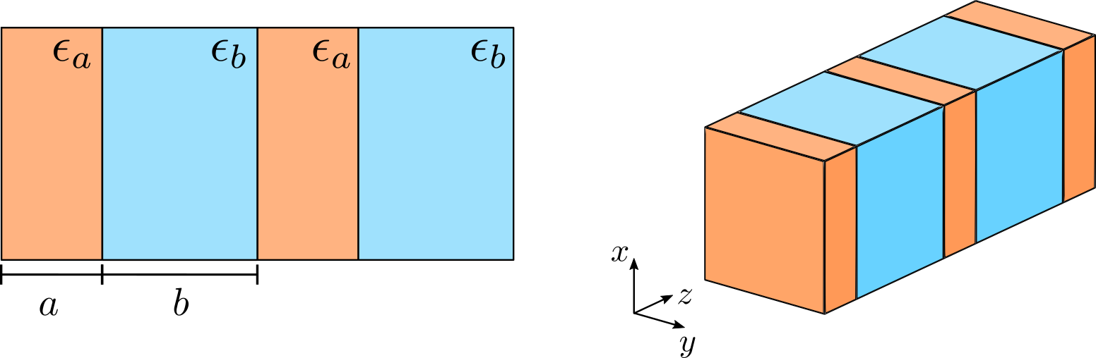
In this section, we derive the electromagnetic field expressions and calculate the photonic bands for an infinite photonic crystal (PC). The representation of the PC is given in Fig. 1. This section contains both few well-known matter, needed to define the physical quantities used throughout the paper, and new results, namely an analytical expression for the photonic bands, .
Based on the Maxwell equations, it is possible to formulate electromagnetism as an eigenvalue problem (Joannopoulos et al., 2008; Skorobogatiy and Yang, 2009). For the magnetic field , the eigenvalue equation reads:
| (1) |
where is the speed of light in vacuum, is the electromagnetic field’s frequency, and is the dielectric function of the photonic crystal unit cell, defined as:
| (2) |
The dielectric function has the periodicity of the photonic crystal, such that , with the period of the crystal. Considering normal incidence only, we write the magnetic field as (Romano et al., 2010):
| (3) |
with the amplitude of the magnetic field. Note that the factor is introduced by mere convenience, since in this way has the dimension of inverse of square root of length, which is convenient for normalization purposes. Inserting (3) into the eigenvalue equation (1) yields a solution in the form:
| (4) |
where and . The electric field follows from the relation:
| (5) |
with vacuum’s dielectric constant. The electric field can thus be written explicitly, in the particular case we are considering, as:
| (6) |
with given by:
| (7) |
Now, we can make use the transfer matrix method (Mora et al., 1985; Romano et al., 2010) to obtain the fields at from their expressions at , that is:
| (8) |
where is the transfer matrix that shifts the fields by inside a slab with dielectric constant , defined as:
| (9) |
This matrix is obtained by explicitly writing two systems of equations: one with and , and another with and . We then use the first system to obtain expressions for the coefficients and . Substituting these into the second system, we arrive at an expression whose left hand side is a column vector consisting of the fields and evaluated at and the right hand side consists of a product of two matrices and a column vector with and evaluated at . This is equivalent to Eq. (8), and the product of these two matrices gives the transfer matrix (see Appendix A for details).
If we now want to move from the origin to the edge of the first unit cell, we write:
| (10) |
Invoking Bloch’s theorem, this can also be written as:
| (11) |
where is Bloch’s momentum. We notice that the matrix is unimodular and, therefore, its eigenvalues are of the form and . Moreover, the trace of a matrix is preserved under unitary transformations, since . Thus, we obtain a transcendental equation for the photonic crystal problem: , which has the following explicit form:
| (12) |
This equation defines the frequency spectrum of the 1D photonic crystal. It is a well known result, an implicit relation for (where enters through and ). Even though can be obtained immediately in terms of , analytical inversion of this relation is not known, so usually Eq. (12) is solved numerically.
II.2 Photonic bands: Analytical results
Having arrived at Eq. (12), we now wish to solve it in order to obtain the photonic band structure. This equation can easily be solved numerically, however, we wish to obtain an analytical expression for . As shown below, with a careful choice of approximations, we can obtain an expression for in total agreement with the numerical solution. The advantage of this is an explicit expression for the band in terms of the photonic crystal parameters, including the calculation of the group velocity, density of states, and band-gap.
Let us start by writing the equality:
with , which is valid for any choice of . Notice that occurs when , that is, this parameter measures the dielectric constant contrast in the crystal. Inserting this relation into Eq. (12) we obtain:
| (13) |
This equation can be solved by iterations using as a small parameter (notice that corresponds to a substantial difference of about 20% between and ). Taking the limit , the first approximation for is easily obtained:
with and . Different combinations of these two indices allow us to describe different bands. While the index controls the band’s vertical position, the index controls its concavity. If is even the band has a bell-like shape; if is odd the bell shape is turned upside-down. For each value of there are two different possible values of . Inserting this first approximation for in the last term of Eq.(13), produces the solution:
| (14) |
where reads:
| (15) |
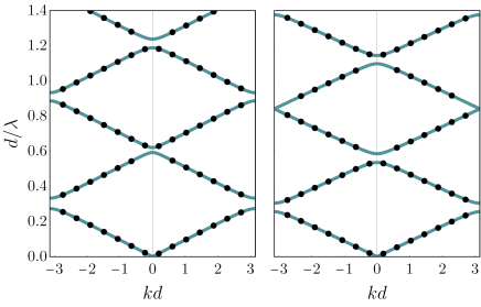
The bands obtained with this expression, as well as the exact results obtained numerically, are plotted in Fig. 2 where it is possible to see an excellent agreement between both approaches; this agreement extends across all the plotted bands. Finally, we note that, although Eq. (14) was obtained after considering the limit , the analytical solution holds even when and are significantly different, as in the case in Fig. 2.
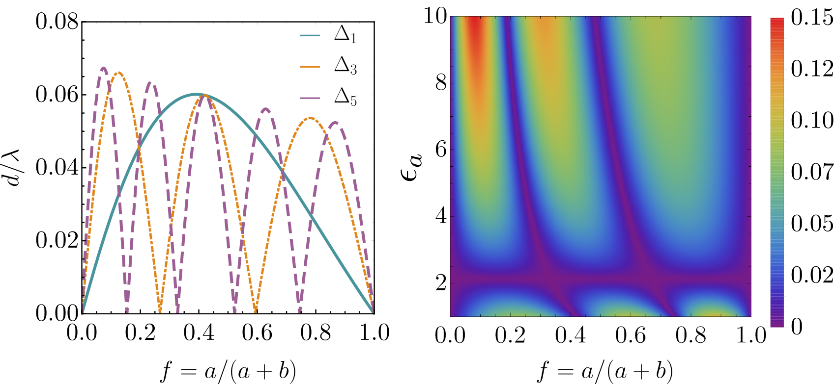
One of the main advantages of obtaining analytical expressions for the bands is the possibility to obtain explicit expressions for the band gaps that enables one to predict under which circumstances will the gaps close and reopen. The analytical expression for the gap between the first two bands reads:
| (16) |
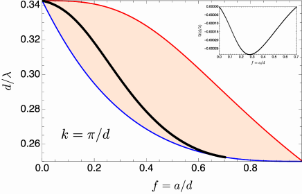
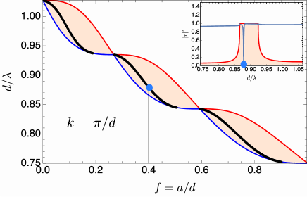
In the limit the band gap vanishes, as expected, since the system becomes an homogeneous medium. Similarly to Eq. (16) we can also obtain analytical expressions for the other gaps. In the left panel of Fig. 3 we plot the first, third and fifth gaps, the first three that open at the edge of the first Brillouin zone, as a function of . There, we can see that all the gaps are closed when and , as expected. Furthermore, the higher energy gaps close more often than the ones below them as we scan through the interval . In the right panel of Fig. 3 we depict the third gap as a function of and for . When either or the gap closes, which is consistent with our previous results. Moreover, we observe that the gap broadens as the difference between the dielectric constants increases and for .
II.3 Determining the fields inside each unit cell
Let us now focus on finding analytical expressions for the electric and magnetic fields . To fully describe the fields across the whole photonic crystal, four coefficients must be determined: , , , and , two for each dielectric slab. In order to obtain the relations between the different coefficients we return to the transfer matrix introduced in Eq. (9), written in the form:
| (17) |
with the entries given in Appendix B. Recalling Eqs. (10) and (11) and explicitly writing and , one obtains the following relation between the coefficients and :
| (18) |
Demanding that the fields must be continuous at , two additional relations appear:
| (19) |
| (20) |
The coefficient is determined from the normalization condition. Therefore, determining is sufficient to entirely describe the fields inside the first unit cell. In fact, we will note compute the actual value of and set it equal to 1 when plots of the fields are presented. To obtain the fields in the rest of the photonic crystal, Bloch’s theorem must be used. If, for example, we wish to obtain the magnetic field in the second unit cell, we need only to multiply the magnetic field defined in the first unit cell by while shifting its argument by , that is .
III Metal-Photonic Crystal Interface
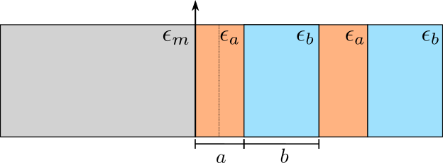
Up to this point, we have dealt with an infinite photonic crystal, determining its band structure as well as the electric and magnetic fields. In this section, we no longer study the problem of an infinite photonic crystal, but rather consider a semi-infinite crystal whose end is connected to a semi-infinite metal, which we will consider to be Silver. Topologically speaking, the silver is a trivial system. We are therefore coupling a trivial system to a photonic crystal with the potential of being topological (this aspect will be addressed in the next section). This new system is depicted in Fig. 4. Our goal is to find the surface states at the metal-photonic crystal interface. These surface states are usually dubbed photonic Tamm states.
We still consider the magnetic field of the form (3) but this time is given by:
| (21) |
with , the metal’s dielectric constant and a coefficient still to be determined. Note that the argument of the exponential for negative guarantees that the field vanishes at large distances. The electric field is once again obtained using Eq. (6). From the continuity of and at , one obtains: and . We now recall that we have already obtained in Eq. (18) an equality that relates with . Substituting this into the previous two equations, and taking the quotient between them we arrive at the following relation:
| (22) |
Therefore, we have two coupled equations, Eqs. (12) and (22), that need to be solve in order to obtain the surface states of the metal-photonic crystal interface. Before doing so, we note that the Bloch momentum of a surface state has the form (Stçélicka, 1974; Ste¸ślicka et al., 1990) , where , and is a complex number owing to the imperfect metal. This number is not related to the one introduced when the analytical expressions for the infinite photonic crystal were presented. A state is called even or odd according to the parity of .
Solving Eqs. (12) and (22) numerically, we obtain solutions in the form of pairs that characterize the surface states of this system. When solving these equations numerically, some non-physical solutions may appear. In order to identify them, some consistency checks must be made: (i) The value of must be positive, since otherwise the fields would diverge as approaches positive infinity, and (ii) must be finite for every () pair, or else Eq. (22) would not be valid. In agreement with the general expectation, all the obtained surface states are located inside the band gaps. Furthermore, we found no more than one state in each gap. In Fig. 5, we depict the energy of the surface states as a function of Analyzing this plot we confirm what was previously stated, the surface states exist only inside the band gaps and there is only one state per gap for a given . Note that in Fig. 5 we have chosen . Had we chosen and no surface state would exist in the limit we choose a highly conducting metallic film. This behavior hints at the existence of two different regimes in the semi-infinite crystal tuned by the value of for fixed (we discuss these two regimes in the context of the SSH-model in Sec. V). Also note that the Tamm states merge to the band-edge when starting to approach the closing of a gap. The more negative the metallic film permittivity is the later the Tamm state merges to the band edge when the closing of a gap is approaching. Also, in the inset of the third panel of Fig. 5we depict the reflectance (blue curve) of a semi-infinite photonic crystal terminated by 34 nm Silver film superimposed on the reflectance (red curve) a purely semi-infinite photonic crystal without the metallic film. The presence of the Tamm state is clearly seen in the former (the full dielectric function of the Silver film was used). The Tamm state is made visible due to the dissipative dielectric function of Silver and coupling to the external photonic modes. Also, in the inset of the first panel we depict the imaginary part of the frequency of the surface-mode existing in the first gap. We see that this quantity is much smaller than the real part of the frequency and, therefore, the mode is weakly damped.
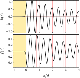
Next, we compute the electric and magnetic fields of the surface states. To do so, we follow the formalism presented in the previous section to construct the fields inside the first unit cell. As was already discussed, to obtain the field in the rest of the crystal, Bloch’s theorem is invoked. In Fig. 6 we present the electric and magnetic fields for a representative surface state. There, we observe that inside the metal both fields decay exponentially away from the origin; inside the photonic crystal the fields oscillate while gradually decaying, although at a lower rate than in the metal. This is characteristic of photonic Tamm states.
IV Topological Aspects of the 1D photonic crystal
Similarly to what occurs in one-dimensional solids, the Bloch functions of the magnetic and electric fields of a 1D photonic crystal pick up a Berry phase when sweeps the Brillouin zone (BZ). If the system presents inversion symmetry, this phase is quantized and it is known as Zak’s phase, assuming the values of or (Zak, 1989) that can be associated to two distinct topological phases. In a periodic quantum mechanical system, the Zak’s phase, , for an isolated band of index can be expressed as the integration of the Berry connection in the BZ, that is, where
| (23) |
and is the Bloch factor for band . Zak’s phase for a gap above band is given by the sum .
One of the simplest examples of 1D systems where one can explore the transition between the topological phases and their physical consequences is the SSH-model that describes electrons hopping in a one dimensional lattice with staggered hopping amplitudes (inter-cell) and (intra-cell). In momentum space, the Bloch Hamiltonian reads , where , , is the Pauli matrix , and is the length of the unit cell. For the system presents a gap separating the two bands. The topology of this gap can be characterized by the Zak phase or, alternatively, by the winding number (Asbóth et al., 2016) that counts the number of times the vector traces out a closed circle around the origin on the plane when Bloch momentum sweeps the Brillouin zone. The ratio defines the topological character of the system.
Although it is tempting to look for a direct analogy between classical waves in periodic systems and 1D periodic quantum systems, one should notice that the formulation of Berry phase and Berry connection in classical waves is somewhat different from the formulation in electronic systems. It is important to establish this formulation before moving into the study of topology in classical waves. A detailed derivation of the Berry phase for electromagnetic waves, including the possibility of magneto-electric coupling is described in Ref. (Onoda et al., 2006). Without magneto-electric coupling, the Berry connection can be written in terms of the Berry connection of electric and magnetic fields as and each contribution (for the 1D case we are considering in this paper) is given by:
| (24) |
where represents complex conjugation, is the (spatial dependent) permittivity for , and is the (spatial dependent) permeability for . The fields and are the periodic parts of the Bloch wave functions of the th photonic band, with wave vector , for the electric and magnetic fields, respectively. Without magneto-electric coupling and one can choose to use either the electric or the magnetic field for the Berry connection calculation. In our calculations, as is homogeneous in the PC, one can consider the magnetic field for the Berry phase calculation.
For a one dimensional system with inversion symmetry, like the SSH-model, the quantized Zak phase depends on the choice of the inversion center in the unit cell, that can also be understood as the way one defines the unit cell containing two different sites. The dependence of the Zak phase on the specific choice of the inversion center seems to lead to an ambiguity in the topological aspect of this model. However, one must recall the bulk-edge correspondence in topological systems. In connection with bulk properties of this model, there are edge states for . Although there are two possible ways of obtaining for the SSH model that depend on the choice of the inversion center, there are also two different ways of cutting the chain. If the chain is cut at the boundary of the unit cell, for example, then for we have and the finite SSH chain presents localized edge states. However, the unit cell could be cut in , which is equivalent to redefining the unit cell with a shift of . In this case, the intercell hopping becomes the intra-cell one and vice versa. Therefore, the system presents and localized edge states for .
In the case of a continuum system such as a photonic crystal, it is possible to produce an edge in an arbitrary part of the unit cell. If one wants to discuss the topology and calculate the Berry phase of the corresponding bulk system, it is necessary to redefine the origin of the unit cell in the location of the cut, similarly to what is done in the SSH model for different types of edges. To exemplify this point, let us consider the semi-infinite PC of Fig. 4: the boundary with the metal is not located at any of the inversion points (one of those signaled by a vertical dashed line) of the bulk crystal and the crystal’s unit cell does not present inversion symmetry. In this case, the possible Berry phases when sweeping the BZ are not quantized (Zak, 1989). However, it is still possible to obtain the Berry phases for arbitrary definitions of the unit cell in terms of the Zak phases for the inversion symmetric unit cells. The non-quantized Berry phases still dictate the topological properties of the system and the existence of edge states in the interface of the PC with other materials. To calculate the Berry phase for the arbitrary unit cell, we first notice that the origin of the unit cell is at distance from the closest inversion center (dashed line in Fig. 4). Let us consider an inversion symmetric unit cell and perform a translation by a distance : . The Bloch functions have to be redefined as . If the new Bloch factors are used in the calculation of the Berry connection of Eq. (24), one gets . After integrating the new Berry connection in the BZ, the Berry phase for an arbitrary definition of the unit cell is given by (Atala et al., 2013) ( the smallest reciprocal lattice vector): . This gives two non-quantized Berry phases and that are related to each other by a phase difference: . Although the difference between the two phases is fixed, their sum varies continuously when varying the ratio , giving rise to a rich phenomenology in multi-band systems.
In particular, for a metal-PC interface, the existence of edge states is determined by the sum in the reflection phases of the metal () embedded in a medium of dielectric function and the PC (); the condition for the existence of an edge state reads: (Silva and Vasilevskiy, 2019; Wang et al., 2016). However, is directly related to the Berry phase of the bulk photonic crystal and consequently it is a function of . This variation gives rise to one edge state per individual gap in Fig. 5.
V Mapping to the SSH-model and the Dirac-like Hamiltonian
In Sec. III we studied a semi-infinite photonic crystal connected to a semi-infinite metal slab. In that configuration we observed the existence of a single Tamm state in each gap, when , and the absence of that state in the opposite regime. Here we make the connection of those results to the SSH-model. We show below that an exact mapping exists between the solutions of Maxwell’s equations of the 1D photonic crystal and the SSH tight-binding model. Once this mapping is established, we show that a Dirac-like Hamiltonian can be written around the band edge thus allowing the connection between the results of Sec. III and topology. Following the procedure described in detail in Appendix C we can show that the solutions of Maxwell’s equations obey, in real space, to the following set of two equations (this result is exact):
| (25) | ||||
| (26) |
which we instantly recognize as a set of tight-binding equations identical to those of the SSH-model (Asbóth et al., 2016), and where the different parameters, , , and entering tight-binding equations are defined as in Eqs. (62)-(66). Clearly, the parameter is an intra-unit-cell hopping and is an inter-unit-cell one. The parameter represents an onsite energy. We should remark, however, that contrary the usual tight-binding parameters in the SSH-model, the parameters , , and are energy dependent. This is essential for obtaining the spectrum condition (12) from the diagonalization of the tight-binding equations. However, since the topological nature of the system is determined by the opening and closing of the gap (leading to band inversion) we can focus our attention in a single gap at the time. Therefore we can expand the tight-binding parameters around the energy at which the gap closes, near (the same arguments apply when the gap closes at ). To be specific, we choose the regime where all gaps close, that is when (), as shown in Fig. 3. Let us focus our attention in the first gap. It closes at a frequency given by when . We can therefore expand the tight-binding parameters around this frequency. This leads to energy-independent hopping parameters and in the form
| (27) | ||||
| (28) |
and with the onsite energy expanded as
| (29) |
with
| (30) |
and
| (31) |
With these relations we arrive at a tight-binding eigenvalue problem of the form:
| (32) | ||||
| (33) |
which maintains its original SSH-model form, but now with energy-independent parameters. Introducing and we obtain:
| (34) |
For having non-trivial solutions for the energy bands the determinant of the previous matrix must be zero, which leads to the following two-band spectrum: , where . This expression for the bands holds near . Considering the eigenvalue problem defined by Eq. (34), we notice that a Dirac-like Hamiltonian can be introduced in the form:
| (35) |
with , and , , and with the Pauli-matrix. This Hamiltonian is valid near the band gap at and for , and satisfies the eigenvalue equation , where stands for the transposition operation. Equation (35) is one of the important results of this paper and allows for the discussion to the topological nature of the end states found in Sec. III. Indeed, it can be shown that the winding number (a topological invariant) is given by (Asbóth et al., 2016)
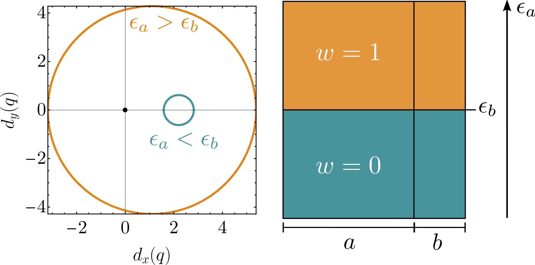
| (36) |
where . It is not difficult to show by direct integration that when the system hosts Tamm states and when it does not. Therefore, the Tamm states we have found in Sec. III are indeed of topological nature. The finiteness of the winding number is best seen in a parametric plot of the vector . The system is topological when the parametric curve encloses the origin and is trivial when it does not. We represent this behavior in Fig. 7 for one example of a topologically non-trivial and a topologically trivial cases. The transition from the topological phase to the trivial phase is controlled, for and fixed, by the relative values of the dielectric constants and . Indeed, if the system is topologically non-trivial, whereas in the opposite regime the system is topologically trivial; this transition is depicted graphically in the right panel of Fig. 7, as a kind of phase diagram.
VI Conclusions
With this work we studied two distinct photonic systems: (i) an infinite photonic crystal and (ii) a semi-infinite PC connected to a semi-infinite metal. For the system (i) we used the transfer matrix method to obtain a transcendental equation that defines the photonic spectrum. Then, with a careful choice of approximations, we obtained analytical expressions for the photonic bands, , and the band gaps, two results not known in the literature two our best knowledge. The analytical results proved to be in excellent agreement with the exact ones obtained numerically, even for large dielectric contrast.
Afterwards, the problem (ii) was tackled with the objective of finding the photonic Tamm states. Imposing boundary conditions for the electric and magnetic fields at the PC surface and combining them with the transcendental equation previously obtained for the case (i), we derived a system of equations whose solution gives the spectrum of the Tamm states. Plotting the frequencies of these states versus , we found that every band gap contained exactly one Tamm state when and none in the opposite case. Had we defined a unit cell with inversion symmetry and cut the crystal at (inversion center), the contact with metal should generate no Tamm states. A simple reasoning for this can be given based on the method of images suitable for a perfect metal, which implies that the semi-infinite crystal reflected with respect to the metal surface, together with the real semi-infinite crystal would form an infinite periodic system without any defect at (Joannopoulos et al., 2008).
Further analysis of Maxwell equations’ solutions allowed us to introduce a tight-binding-type Hamiltonian that is a variant of the SSH model and to analyze it from the topology point of view. It is probably the central result of this work. From the SSH model, a Dirac-like Hamiltonian representation of the bulk states near the band edge, where the band gap closes, was introduced. With this representation at hand, the winding number was computed and two topologically different situations have been distinguished: (1) a topologically non-trivial phase for , and (2) a topologically trivial one in the opposite case. Although we have cast the analysis of the topological nature of the Tamm states in terms of the winding number, we could also have analyzed the problem in terms of the Zak phase (Zak, 1989; Gao et al., 2017; Vanderbilt, 2018; Wang et al., 2019) of the bands, which can be accessed via reflection measurements (Gao et al., 2015). Indeed, we can compute the Zak phase for the first two bands and find and when and , and when and if choosing a mirror symmetric unit cell (see discussion in Sec. IV). These results mean that in the first case the gap has a topological nature, whereas in the second regime it is a topologically trivial gap (same Zak phase in both bands).
We did not include the effect of dissipation in the photonic crystal (although we did that for the metal) for two reasons. Firstly, the materials we are using in the model, HfO2 and SiO2, have negligible dissipation in the visible spectral range. Secondly, the main effect of taking it into account would be adding a small imaginary part to either wavevector or frequency but no significant changes in the spectrum should be expected as long as (see, however, Ref. (Wolff et al., 2018) for a detailed study of the role of dissipation in photonic systems). The effect of damping in the metal (imaginary part of the dielectric function of Silver) is best seen in the reflectance of the finite metal film on top of the semi-infinite photonic crystal (results shown in the inset of Fig. 5). The damping makes the Tamm state clearly visible as a dip in the reflectance spectrum. One possible way to overcome damping is to use a symmetric system where the losses are compensated by the gain (Mortensen et al., 2018).
Finally, we have not studied the case of a finite transverse momentum. This would make de Tamm states dispersive along the transverse direction, with some "effective mass" (Kaliteevski et al., 2007; Silv2019). Its detailed analysis will be the focus of a forthcoming publication.
Acknowledgements.
N.M.R.P., M.I.V., and Y.V.B. acknowledge support from the European Commission through the project “Graphene-Driven Revolutions in ICT and Beyond” (Ref. No. 785219) and the Portuguese Foundation for Science and Technology (FCT) in the framework of the Strategic Financing UID/FIS/04650/2019. N.M.R.P., T.G.R., and Y.V.B. acknowledge COMPETE2020, PORTUGAL2020, FEDER and the Portuguese Foundation for Science and Technology (FCT) through project and POCI-01-0145-FEDER-028114. The authors acknowledge André Chaves for suggesting the starting point of the analytical approach to the photonic bands. N.M.R.P. acknowledges stimulating discussions with Joaquin Fernandéz-Rossier on the topic of the paper. J.C.G.H. acknowledges the hospitality of the Physics Department of SDU, Denmark, where this work was completed. The authors are thankful to Asger Mortensen and Mário Silveirinha for their careful and critical reading of the manuscript.Appendix A Derivation of the transfer matrix
Within a slab of constant we have the following relation for the fields and the expansion coefficients and :
| (37) |
and
| (38) |
From the previous two equations we can eliminate the vector composed of the coefficients and . Inverting the last equation follows
| (39) |
which leads to
| (40) |
which can be written as
| (41) |
where is the transfer matrix within the region of constant . If we now want to connect two regions of different , where the one to the left is and the subsequent one is , we must have
| (42) |
The product defines the transfer matrix across the unit cell.
Appendix B Transfer matrix elements
In this Appendix we briefly present the expressions for the different entries of the transfer matrix given in Eq. (17):
| (43) | ||||
| (44) | ||||
| (45) | ||||
| (46) |
Appendix C Derivation of the tight-binding electromagnetic model
Here we give the details of the derivation of the tight-binding electromagnetic model, showing the existence of an exact mapping between the solutions of Maxwell’s equations and the SSH model. To do so, we recall the definition of the electric and magnetic fields presented in the main text:
| (47) |
with
| (48) |
where ; and:
| (49) |
which written explicitly reads:
| (50) |
with
| (51) |
Our goal is to obtain and from their values at the interfaces between dielectric slabs. To this end, we use the transfer matrix presented in Eq. (9) to write:
| (52) |
which gives us and on the interface between slabs and of the th unit cell from their values at the origin of the th unit cell; and:
| (53) |
which relates the fields at with their values at the origin of the th unit cell. From these two equations one obtains the following expressions for and :
| (54) |
and
| (55) |
Following an analogous procedure for the other dielectric slab, we write:
| (56) |
| (57) |
Once again, this allows us to obtain expressions for and from their values at the interfaces:
| (58) |
and
| (59) |
We now impose the continuity of the electric and magnetic fields at and at , from where we obtain:
| (60) |
| (61) |
Note that the second equation involves both the and the th unit cells. To simplify these expressions we introduce the following quantities:
| (62) | ||||
| (63) | ||||
| (64) | ||||
| (65) | ||||
| (66) |
Using this new notation, Eqs. (60) and (61) become:
| (67) | ||||
| (68) |
We now note that these equations are those defining the SSH model in real space, i.e. a tight-binding approximation but with energy dependent hopping parameters and , and onsite energy .
References
- Wang and Zhang (2017) J. Wang and S. Zhang, Nature Mater. 16, 1062 (2017).
- Belopolski et al. (2017) I. Belopolski, S.-Y. Xu, N. Koirala, C. Liu, G. Bian, V. N. Strocov, G. Chang, M. Neupane, N. Alidoust, D. Sanchez, H. Zheng, M. Brahlek, V. Rogalev, T. Kim, N. C. Plumb, C. Chen, F. Bertran, P. Le Fèvre, A. Taleb-Ibrahimi, M.-C. Asensio, M. Shi, H. Lin, M. Hoesch, S. Oh, and M. Z. Hasan, Science Advances 3, e1501692 (2017).
- Yang et al. (2019) C. N. Yang, M.-L. Ge, and Y.-H. He, Topology in Physics, 1st ed. (World Scientific, Singapore, 2019).
- Yan et al. (2015) B. Yan, B. Stadtmuller, N. Haag, S. Jakobs, J. Seidel, D. Jungkenn, S. Mathias, M. Cinchetti, M. Aeschlimann, and C. Felser, Nat. Commun. 6, 10167 (2015).
- Xie et al. (2018) B.-Y. Xie, H.-F. Wang, X.-Y. Zhu, M.-H. Lu, Z. D. Wang, and Y.-F. Chen, Opt. Express 26, 24531 (2018).
- Rider et al. (2019) M. S. Rider, S. J. Palmer, S. R. Pocock, X. Xiao, P. Arroyo Huidobro, and V. Giannini, J. App. Phys. 125, 120901 (2019).
- Ozawa et al. (2019) T. Ozawa, H. M. Price, A. Amo, N. Goldman, M. Hafezi, L. Lu, M. C. Rechtsman, D. Schuster, J. Simon, O. Zilberberg, and I. Carusotto, Rev. Mod. Phys. 91, 015006 (2019).
- (8) S. V. Silva, D. E. Fernandes, T. A. Morgado, and M. G. Silveirinha, “Fractional chern numbers and topological pumping in photonic systems,” arXiv:1912.11271 .
- Murakami (2011) S. Murakami, New J. Phys. 13, 105007 (2011).
- Vafek and Vishwanath (2014) O. Vafek and A. Vishwanath, Annu. Rev. Condens. Matter Phys. 5, 83 (2014).
- Khanikaev and Shvets (2017) A. B. Khanikaev and G. Shvets, Nat. Photonics 11, 763 (2017).
- Downing and Weick (2017) C. A. Downing and G. Weick, Phys. Rev. B 95, 125426 (2017).
- Bleckmann et al. (2017) F. Bleckmann, Z. Cherpakova, S. Linden, and A. Alberti, Phys. Rev. B 96, 045417 (2017).
- Pocock et al. (2018) S. R. Pocock, X. Xiao, P. A. Huidobro, and V. Giannini, ACS Photonics 5, 2271 (2018).
- Whittaker et al. (2019) C. E. Whittaker, E. Cancellieri, P. M. Walker, B. Royall, L. E. Tapia Rodriguez, E. Clarke, D. M. Whittaker, H. Schomerus, M. S. Skolnick, and D. N. Krizhanovskii, Phys. Rev. B 99, 081402 (2019).
- Zhang et al. (2019) Z. Zhang, M. H. Teimourpour, J. Arkinstall, M. Pan, P. Miao, H. Schomerus, R. El-Ganainy, and L. Feng, Laser & Photonics Reviews 13, 1800202 (2019).
- Xiao et al. (2015) M. Xiao, G. Ma, Z. Yang, P. Sheng, Z. Q. Zhang, and C. T. Chan, Nature Phys. 11, 240 (2015).
- Li et al. (2018) X. Li, Y. Meng, X. Wu, S. Yan, Y. Huang, S. Wang, and W. Wen, App. Phys. Lett. 113, 203501 (2018).
- Jiang et al. (2018) J. Jiang, Z. Guo, Y. Ding, Y. Sun, Y. Li, H. Jiang, and H. Chen, Opt. Express 26, 12891 (2018).
- Kane and Lubensky (2014) C. Kane and T. Lubensky, Nature Phys. 10, 39 (2014).
- Watson (1996) G. Watson, Contemporary Physics 37, 127 (1996).
- Delplace et al. (2011) P. Delplace, D. Ullmo, and G. Montambaux, Phys. Rev. B 84, 195452 (2011).
- Rhim et al. (2017) J.-W. Rhim, J. Behrends, and J. H. Bardarson, Phys. Rev. B 95, 035421 (2017).
- Thouless et al. (1982) D. J. Thouless, M. Kohmoto, M. P. Nightingale, and M. den Nijs, Phys. Rev. Lett. 49, 405 (1982).
- Kohmoto (1985) M. Kohmoto, Annals of Physics 160, 343 (1985).
- Kalozoumis et al. (2018) P. A. Kalozoumis, G. Theocharis, V. Achilleos, S. Félix, O. Richoux, and V. Pagneux, Phys. Rev. A 98, 023838 (2018).
- Meier et al. (2018) E. J. Meier, F. A. An, A. Dauphin, M. Maffei, P. Massignan, T. L. Hughes, and B. Gadway, Science 362, 929 (2018).
- Kronig and Penney (1931) R. d. L. Kronig and W. G. Penney, Proceedings of the Royal Society of London. Series A 130, 499 (1931).
- McQuarrie (1996) D. A. McQuarrie, The Chemical Educator 1, 1 (1996).
- Szmulowicz (1997) F. Szmulowicz, European Journal of Physics 18, 392 (1997).
- Mishra and Satpathy (2003) S. Mishra and S. Satpathy, Phys. Rev. B 68, 045121 (2003).
- Su et al. (1980) W. P. Su, J. R. Schrieffer, and A. J. Heeger, Phys. Rev. B 22, 2099 (1980).
- Heeger et al. (1988) A. J. Heeger, S. Kivelson, J. R. Schrieffer, and W. P. Su, Rev. Mod. Phys. 60, 781 (1988).
- Li et al. (2014) L. Li, Z. Xu, and S. Chen, Phys. Rev. B 89, 085111 (2014).
- Liu et al. (2018) F. Liu, H.-Y. Deng, and K. Wakabayashi, Phys. Rev. B 97, 035442 (2018).
- Obana et al. (2019) D. Obana, F. Liu, and K. Wakabayashi, Phys. Rev. B 100, 075437 (2019).
- Xie et al. (2019) D. Xie, W. Gou, T. Xiao, B. Gadway, and B. Yan, npj Quantum Inf. 5, 55 (2019).
- Ste¸ślicka et al. (1990) M. Ste¸ślicka, R. Kucharczyk, and M. L. Glasser, Phys. Rev. B 42, 1458 (1990).
- Istrate et al. (2005) E. Istrate, A. A. Green, and E. H. Sargent, Phys. Rev. B 71, 195122 (2005).
- Xiao et al. (2014) M. Xiao, Z. Q. Zhang, and C. T. Chan, Phys. Rev. X 4, 021017 (2014).
- Liu (1997) N.-h. Liu, Phys. Rev. B 55, 4097 (1997).
- Wang et al. (2009) T.-B. Wang, C.-P. Yin, W.-Y. Liang, J.-W. Dong, and H.-Z. Wang, J. Opt. Soc. Am. B 26, 1635 (2009).
- Bello et al. (2019) M. Bello, G. Platero, J. I. Cirac, and A. González-Tudela, Science Advances 5, eaaw0297 (2019).
- El-Ganainy and Levy (2015) R. El-Ganainy and M. Levy, Opt. Lett. 40, 5275 (2015).
- Han et al. (2015) C. Han, M. Lee, S. Callard, C. Seassal, and H. Jeon, Light Sci. App. 8, 40 (2015).
- Ota et al. (2018) Y. Ota, R. Katsumi, K. Watanabe, S. Iwamoto, and Y. Arakawa, Commun. Phys. 1, 86 (2018).
- Gomez et al. (2017) D. E. Gomez, Y. Hwang, J. Lin, T. J. Davis, and A. Roberts, ACS Photonics 4, 1607 (2017).
- Pocock et al. (2019) S. R. Pocock, P. A. Huidobro, and V. Giannini, Nanophotonics 8, 1337 (2019).
- Jiang et al. (2020) Z. Jiang, M. Rosner, R. E. Groenewald, and S. Haas, Phys. Rev. B 101, 045106 (2020).
- Sun et al. (2017) X.-C. Sun, C. He, X.-P. Liu, M.-H. Lu, S.-N. Zhu, and Y.-F. Chen, Progress in Quantum Electronics 55, 52 (2017).
- Asbóth et al. (2016) J. K. Asbóth, L. Oroszlány, and A. Pályi, A Short Course on Topological Insulators, 1st ed. (Springer, New York, 2016).
- Tamm (1932) I. E. Tamm, Physik. Z. Sovjetunion 1, 733 (1932).
- Kaliteevski et al. (2007) M. Kaliteevski, I. Iorsh, S. Brand, R. A. Abram, J. M. Chamberlain, A. V. Kavokin, and I. A. Shelykh, Phys. Rev. B 76, 165415 (2007).
- Sasin et al. (2010) M. E. Sasin, R. P. Seisyan, M. A. Kaliteevski, S. Brand, R. A. Abram, J. M. Chamberlain, I. V. Iorsh, I. A. Shelykh, A. Y. Egorov, A. P. Vasil’ev, V. S. Mikhrin, and A. V. Kavokin, Superlattices and Microstructures 47, 44 (2010).
- Núnez-Sánchez et al. (2016) S. Núnez-Sánchez, M. Lopez-Garcia, M. M. Murshidy, A. G. Abdel-Hady, M. Serry, A. M. Adawi, J. G. Rarity, R. Oulton, and W. L. Barnes, ACS Photonics 3, 743 (2016).
- Silva and Vasilevskiy (2019) J. M. S. S. Silva and M. I. Vasilevskiy, Optical Materials Express 9, 244 (2019).
- Joannopoulos et al. (2008) J. D. Joannopoulos, S. G. Johnson, J. N. Winn, and R. D. Meade, Photonic Crystals, 2nd ed. (PUP, New Jersey, 2008).
- Skorobogatiy and Yang (2009) M. Skorobogatiy and J. Yang, Fundamentals of Photonic Crystal Guiding, 1st ed. (CUP, Cambridge, 2009).
- Romano et al. (2010) M. C. Romano, D. R. Nacbar, and A. Bruno-Alfonso, J. Phys. B: At. Mol. Opt. Phys. 43, 215403 (2010).
- Mora et al. (1985) M. Mora, R. Pérez, and C. B. Sommers, Journal de Physique 46, 1021 (1985).
- Stçélicka (1974) M. Stçélicka, Progress in Surface Science 5, 157 (1974).
- Zak (1989) J. Zak, Phys. Rev. Lett. 62, 2747 (1989).
- Onoda et al. (2006) M. Onoda, S. Murakami, and N. Nagaosa, Phys. Rev. E 74, 066610 (2006).
- Atala et al. (2013) M. Atala, M. Aidelsburger, J. T. Barreiro, D. Abanin, T. Kitagawa, E. Demler, and I. Bloch, Nature Physics 9, 795 (2013).
- Wang et al. (2016) Q. Wang, M. Xiao, H. Liu, S. Zhu, and C. T. Chan, Phys. Rev. B 93, 041415 (2016).
- Gao et al. (2017) W. Gao, M. Xiao, B. Chen, E. Y. B. Pun, C. T. Chan, and W. Y. Tam, Opt. Lett. 42, 1500 (2017).
- Vanderbilt (2018) D. Vanderbilt, Berry Phases in Electronic Structure Theory, 1st ed. (CUP, Cambridge, 2018).
- Wang et al. (2019) H.-X. Wang, G.-Y. Guo, and J.-H. Jiang, New J. Phys. 21, 093029 (2019).
- Gao et al. (2015) W. S. Gao, M. Xiao, C. T. Chan, and W. Y. Tam, Opt. Lett. 40, 5259 (2015).
- Wolff et al. (2018) C. Wolff, K. Busch, and N. A. Mortensen, Phys. Rev. B 97, 104203 (2018).
- Mortensen et al. (2018) N. A. Mortensen, P. A. D. Gonçalves, M. Khajavikhan, D. N. Christodoulides, C. Tserkezis, and C. Wolff, Optica 5, 1342 (2018).