Gate-controlled Spin Extraction from Topological Insulator Surfaces
Abstract
Spin-momentum locking, a key property of the surface states of three-dimensional topological insulators (3DTIs), provides a new avenue for spintronics applications. One consequence of spin-momentum locking is the induction of surface spin accumulations due to applied electric fields. In this work, we investigate the extraction of such electrically-induced spins from their host TI material into adjoining conventional, hence topologically trivial, materials that are commonly used in electronics devices. We focus on effective Hamiltonians for bismuth-based 3DTI materials in the family, and numerically explore the geometries for extracting current-induced spins from a TI surface. In particular, we consider a device geometry in which a side pocket is attached to various faces of a 3DTI quantum wire and show that it is possible to create current-induced spin accumulations in these topologically trivial side pockets. We further study how such spin extraction depends on geometry and material parameters, and find that electron-hole degrees of freedom can be utilized to control the polarization of the extracted spins by an applied gate voltage.
pacs:
Valid PACS appear hereI Introduction
The push towards the utilization of the electron’s spin degree of freedom in common electronic devices, which are conventionally based on the manipulation of the electron charge, has matured to the field called spintronics vzutic2004spintronics . The various lines of research in this field not only comprise questions of fundamental interest in spin physics, but also focus on applications. Possible advantages of utilizing spin-based elements in comparison to charge-based electronic devices might be low power consumption and less heat dissipation, as well as more compact and faster reading/writing of data.
The ferromagnets ralph2008spin ; wolf2001spintronics ; sato2002first are the mainstream materials used in spintronics where the ferromagnetic exchange interaction causes the spin-dependency of transport, allowing the creation/manipulation/detection of spins. However, after the celebrated Datta-Das spin transistor proposal datta1990electronic , it became clear that spin-orbit interaction can also be utilized for spin manipulation in electronic devices. As the Datta-Das setting still requires ferromagnetic leads, a parallel approach utilizing materials without intrinsic magnetism, such as paramagnetic metals and semiconductors with only spin-orbit coupling awschalom2013semiconductor ; kato2004observation ; Schliemann2017 , has become an attractive alternative.
Various methods of spintronics implementations without ferromagnets have emerged and developed over the recent years edelstein1990spin ; inoue2003diffuse ; silov2004current ; ganichev2004can; ganichev2006electric ; d1971possibility ; dyakonov1971current ; hirsch1999spin ; governale2003pumping ; mal2003spin ; murakami20042 ; Scheid-et-al . These methods are commonly based on (i) the spin Hall effect dyakonov1971current , where an applied electric current generates a transverse spin current, and (ii) Edelstein (or inverse spin galvanic) effect edelstein1990spin ; aronov1989 , where an applied electrical current generates a nonzero spin accumulation. Once generated, as these spins drive spintronics circuits, they need to be further manipulated and ultimately detected. For detection, inverse effects corresponding to those mentioned above, namely the inverse spin Hall effect saitoh2006conversion ; kimura2007room ; uchida2008observation ; valenzuela2006direct ; seki2008giant and spin galvanic effect (SGE) ganichev2002 ; sanchez2013spin ; adagideli2007extracting ; vzutic2002spin ; shen2014microscopic have been successfully utilized. Main methods for spin manipulation are based on exchange and Zeeman fields or spin-orbit coupling to induce spin precession. However, weak coupling requires long length scales over which the induced spins need to remain coherent. This is an issue as spin precession lengths are usually comparable to spin relaxation/dephasing lengths. Furthermore, the spin-orbit coupling needs to be controlled over the precession (hence manipulation) region, while spin-generation in part of the circuit needs to remain unaffected. Hence in order to close the creation/manipulation/detection cycle reliably, additional electrical methods for spin manipulation is desirable.
In this work, we consider a mechanism in TIs that allows for local and all-electrical control of electrically generated spins with gates. In most spintronics (or spin-orbitronics) platforms, charge carriers are of a given type: either electron or hole, implying that local application of gates equally couples to both spin species. In others where electron and hole pockets might co-exist, there is no coherence between the electron/hole degree of freedom and the spin degree of freedom. As a consequence, electric gates cannot locally control local spin accumulations in conventional spintronics and spin-orbtronics platforms. On the other hand, the surface (or edge) of 3D (2D) TIs feature both electron- and hole degrees of freedom as well as spin-orbit coupling. Applied gates control the local potential, which couples oppositely to electrons and holes, and spin-orbit coupling allows for spin dependency of electron-hole degrees of freedom. We demonstrate below that this joint property allows for electronic control of spins locally within a region much smaller than the spin precession length, the lengthscale over which spins can be manipulated in conventional spintronics applications vzutic2004spintronics .
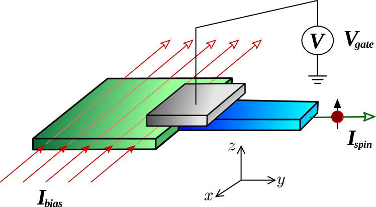
As an explicit example, we consider 3DTI materials of the family whose effective model is extensively discussed in the literature Zhang ; zhang2012 ; silvestrov2012 ; brey2014 . Qualitatively, our conclusions should apply also to strained (3D) HgTe, though an equally successful effective model for such a system is still missing. We focus on a particular geometry (sketched in Fig. 1) and demonstrate how the spin extraction can be controlled in a region smaller than the spin precession length. In this geometry, the spins are generated by the spin galvanic effect at the surface of the TI. By attaching a side pocket and tuning the chemical potential on the pocket by an applied gate voltage, we demonstrate that the extracted spins can change their polarization, regardless of the generated spins on the TI side.
Our paper is organized as follows: In Sec. II.1, we outline the effective surface Hamiltonian of a 3DTI and the corresponding spin operators. We then present the inverse spin galvanic effect (ISGE), also known as Edelstein effect, through Kubo formalism in Sec. II.2. Different names addressing the same phenomenon are used in the literature depending on context. In Sec. II.3, we state an ISGE paradox with its solution for the surfaces of a 3DTI. Next, we discuss the model and the method proposed for extracting spin from surfaces of a 3DTI in Sec. III.1. In Sec. III.2, we derive the spin behavior on the 3DTI surfaces, which we show to be in close agreement with our numerical simulations. In Sec. III.3, we demonstrate how to extract spins from 3DTI surfaces and how to manipulate their polarization through a gate potential. We close with concluding remarks in Sec. IV.
II A spin-galvanic paradox and its solution
II.1 Setting the stage
Consider a finite crystal of an anisotropic 3DTI material, such as , which in its TI phase hosts topologically protected metallic surface states. The existence of these states, described by a single Dirac cone, were confirmed experimentally by ARPES chen2009experimental ; xia2009observation and STS alpichshev2010stm ; zhang2009experimental ; cheng2010landau ; hanaguri2010momentum ; alpichshev2011stm measurements. Further experiments confirmed the helical nature of such surface states hsieh2009observation . The anisotropy of these materials implies that the topological metallic states existing on the different crystal faces will be described by Dirac-like effective Hamiltonians featuring different spin structures zhang2012 ; silvestrov2012 ; brey2014 . We are interested in the consequences of the anisotropy of these materials on the ISGE aronov1989 ; ivchenko1990current ; edelstein1990spin , for recent discussions see ganichev2016 ; gorini2017 ; ando2017 .
The states of the 2D helical surfaces of are admixtures of electron- and hole-like states of different parity () and spin (), coming from Bi and Se -orbitals, and , respectively Zhang . As a consequence, the real spin content of such states does not necessarily coincide with the pseudospin degrees of freedom used to label them. Hence, () denote the Pauli operators corresponding to the two bands at the surface (the pseudospin), while are the spin operators within this restricted Hillbert space. The most commonly “known” low-energy effective Hamiltonian for the topological surface state is that of the “top” and “bottom” surfaces in the growth direction, which we choose to be in the direction:
| (1) |
where is the energy of the Dirac point, is the corresponding Fermi velocity and refers to the surface normals pointing away the bulk. In this case the spin and the pseudospin operators are the same:
| (2) |
This identification as well as the rotational symmetry, however is lost at the side surfaces:
| (3) |
where is the energy of the Dirac point, and and are the corresponding Fermi velocity in the and directions, respectively. In this case, while the component of the spin and the pseusospin operators are the same, they are merely proportional in the and surfaces with the proportionality parameter :
| (4) |
For completeness, we express the surface Hamiltonian as
| (5) |
| (6) |
where , and are the Fermi velocities in the and directions, respectively. To summarize, the real spin coincides with the Pauli matrices of the pseudospin only on the surface. In particular, if , the surface states on the side have . This point is crucial, as we discuss below.
II.2 Spin galvanic basics
We consider the spin accumulation, , generated in response to an applied electric field in a spin-orbit coupled 2D system lying in the - plane – corresponding to the side surfaces . The ISGE can be written in Kubo form inoue2003diffuse as
| (7) | |||||
| (8) |
where is the Kubo linear response kernel, is the vector potential and is the frequency-dependent ISGE conductivity. Thus
| (9) |
Its Onsager reciprocal effect, the spin galvanic effect (SGE), reads shen2014microscopic
| (10) | |||||
| (11) |
yielding
| (12) |
In Eq. (11) is the time derivative of the magnetic field which generates the non-equilibrium leading to the SGE.
II.3 Spin galvanic effect on the surface of a 3DTI
As we stressed above, the relation between the pseudospin and the real spin on the 3DTI surface can be anisotropic. The two quantities are identical on the surfaces, and hence there is no ambiguity in calculating the ISGE and the SGE on the surfaces. However, on the surfaces
| (13) |
On the surface of the TI, spin and charge/momentum are locked. To be explicit we assume
| (14) |
with is the Fermi velocity in the -direction (see Eqs. (1)-(3)). From Eqs. (13) and (14) one gets
| (15) |
Equation (15) seems to imply a divergent (“colossal”) SGE for , while the ISGE should vanish.
This apparent paradox is resolved by judiciously inspecting the SGE and ISGE linear response kernels. First, for the SGE one has
| (16) | |||||
| (17) |
which tends to zero for as it should: The pseudospin-pseudospin response function defined above has no divergencies. Similarly for the ISGE holds
| (18) | |||||
| (19) |
which is given by the same response function and again vanishes in the limit.
III Spin extraction from 3DTI surfaces
Even though it turns out that there is no paradox in the form of a divergent SGE response, there are interesting consequences when considering . In particular, as we show below, it is possible to extract current-induced spins from the side surfaces even if these are not spin polarized. The main idea is the following: at the side surfaces of a TI, an analytical examination of the non-equilibrium population of the states (induced by, say, an applied bias) reveals their composition to be a mixture of spin-up electron-like and a spin-down hole-like quasiparticles whose spins partially cancel each other. This is the origin of the parameter in general. In the limit (hence ) the cancellation is perfect. Therefore, it suffices to contact the surface with a “pocket” containing electrons or holes–in practice, a gated semiconductor–so that only the spin-polarized electron- or hole-like part of the surface state will leak out of the TI. A side pocket/lead thus acts as a gate-tunable spin extractor: The sign of the extracted spins can be reversed by simply switching the pocket polarity from - to -type or vice versa, allowing for local electrical control of spin polarization. Note the crucial observation that the size of the region where the spin is reversed can be shorter than the spin precession length (see Fig. 7 below).
III.1 Model and method
In the rest of this Section, we further study the spin extraction effect through analytical and numerical means for 3DTI nanowires. The wires are described by a 3D effective Hamiltonian which captures the basic low-energy properties of family, including e.g. , and materials Zhang ; liu2010model :
| (20) | |||||
where
Here, and are the Pauli matrices, and and are the identity matrices in spin and orbital space, respectively. If then the system is in the topologically nontrivial phase and Dirac-like surface states form within the bulk band gap. For a wire, due to the size quantization around the wire, the surface states form 1D channels and the lowest 1D subband is gapped due to its non-trivial Berry phase bardarson2010 ; ziegler2018 .
In order to find the current-induced spin polarization on the 3DTI nanowire surfaces, we need the spin operators expressed in the basis used to represent Eq. (20). The basis states are hybridized states of the Se and Bi orbitals with even () and odd () parities, and spins up () and down (), namely , , , , in that order. Then the spin operators in the basis of bulk states are given by brey2014 :
| (21) |
Using the explicit forms of the spin operators, Eqs. (21), we generalize the Kubo response kernel of effective 2D surface model of the previous section to the more realistic 3D model (20):
| (22) | |||||
| (23) |
with .
The effective surface description is obtained by projecting in to the space spanned by the surface modes. One thus obtains the effective surface spin and Hamiltonian operators (see Appendix A). These surface Hamiltonians and modes for electrons on 3DTI faces defined by their normals , were computed by Brey and Fertig brey2014 . In our geometry, the relevant surfaces are and where the projections of the spin operators follow Eq. (2) and Eq. (4), yielding the effective Hamiltonians Eq. (1) and Eq. (3), respectively. The parameters of surface Hamiltonians are then obtained from Eq. (20) brey2014 by projection. In particular, the band crossing energies of the and surfaces (which are the relevant surfaces for our choice of axes) are given by:
| (24) | ||||
| (25) |
and the corresponding Fermi velocities are given by:
| (26) | ||||
| (27) | ||||
| (28) |
where
| (29) |
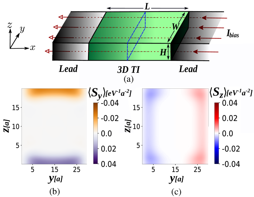
In our numerical study, we use the tight-binding representation of the Hamiltonian in Eq. (20) and focus on a a 3DTI wire attached to two semi-infinite leads (see Fig. 2(a)). We evaluate nonequilibrium local spin densities for each site , where is the wavefunction of the (occupied) state at site and are the spin operators defined in Eq. (21). We then sum over all occupied states . For an infinitesimal bias, these are all scattering wavefunctions at a certain energy, originating from one of the leads, depending on the sign of the bias. Local charge density is similarly obtained when . We utilize the KWANT toolbox groth2014kwant for our numerical simulations. The parameters of our band Hamiltonian are chosen from ab-initio band structure calculations of liu2010model in our numerical simulations. The particular values used are , , , , , , and . We have also set the lattice constant to be in our numerical calculations.
III.2 Spin dynamics and accumulation at the surface
As a consequence of the locking of the spin and the momentum of the surface states in 3DTIs, the dynamics of spin and charge distributions are coupled. Moreover, even nonmagnetic impurities can flip an electron’s spin during scattering, leading to the dominant spin relaxation mechanism –a variant of the Dyakonov-Perel spin relaxation dyakonov1972spin . All these are summarized by the spin diffusion equations, valid at lengthscales much larger than the mean free path, that describes the coupled dynamics of spin and charge. For the top () surface of the TI, the relevant diffusion equations are given by burkov2010spin :
| (30) | |||||
where is the totally antisymmetric tensor, is the diffusion constant which is proportional to mean free time, , and Fermi velocity, (for surface, ). are the components of the pseudospin nonequilibrium density, , is the charge density and refers to the top and bottom surfaces. In order to apply Eq. (III.2) to the side surfaces, (, see Appendix B), we generalize the diffusion equations to anisotropic surfaces and obtain how the accumulated real spins depend on the charge gradients due to applied voltage bias:
| (31) | |||||
| (32) |
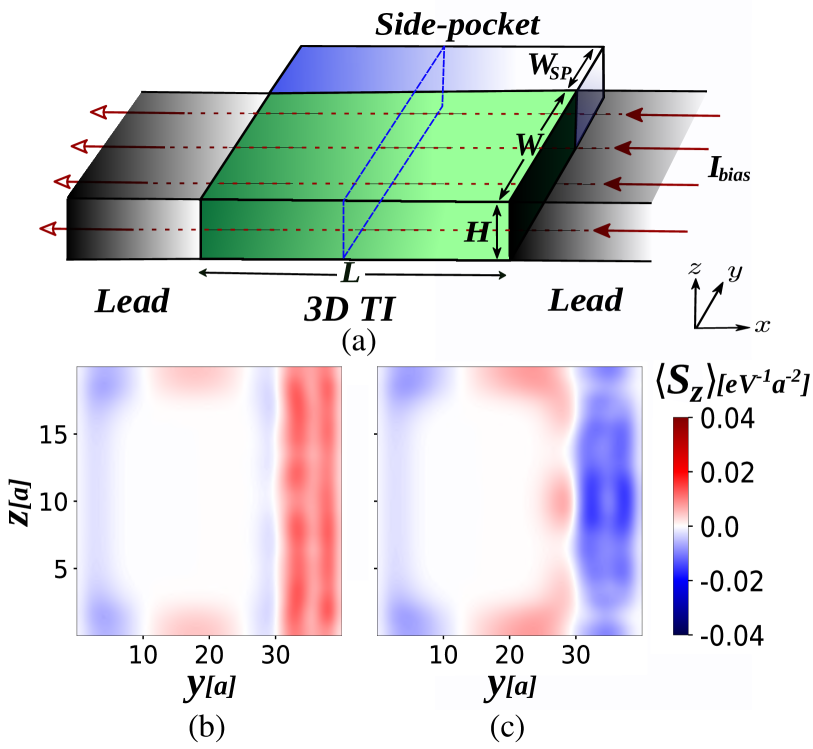
Hence, if sits in the bulk gap, then applying a bias voltage yields surface currents flowing in the -direction, which in turn induces spin accumulations on the and the surfaces. This is the ISGE. In order to test these predictions, we numerically obtain spin densities via the method described in Sec. III.1. Our results are shown in Figs. 2(b) and 2(c), where we plot the -averaged cross-sectional profile for and . Note that both components of the spin accumulation are localized to the respective surfaces and have opposite sign on opposite surfaces. Notice also that in our configuration since it is along the current direction. Furthermore, is smaller than for . The case , as mentioned earlier, corresponds to a vanishing ISGE and the “paradoxical” regime of Sec. II.
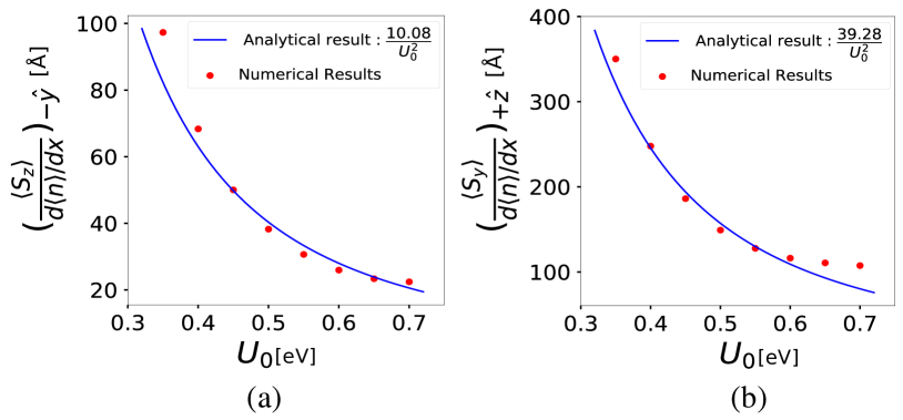
In order to test Eqs. (31) and (32) numerically, we consider the quotient on the left hand side of these equations as a function of disorder strength . Since in the golden rule regime , we expect a behavior. In order to get the exact relation, we analytically calculate the mean free time using a approximation for surface eigenmodes in Appendix B. Next, we perform numerical simulations and obtain the local spin/charge accumulations and avearge these over a square region in the middle of the and surfaces as well as over different disorder configurations with strength . Finally, we compare our analytical prediction (the blue line) for the left-hand-sides of Eqs. (31) and (32) against the numerical simulations (red dots) in Figs. LABEL:fig:szoverdnpart and LABEL:fig:syoverdnpart, respectively. We find that our numerical results for ISGE are well described by the analytical formulas in Eqs. (31) and (32).
III.3 Spin extraction
Having discussed how spins can be induced at a topological insulator surface, we now study how these spins can be extracted to be used in (presumably topologically trivial) spintronics circuitry. To this end, we focus on a geometry where a topologically trivial side pocket is attached to the TI nanowire (see Figs. 4(a) and 5(a)). The current-induced spins at the TI surface can then leak into the side pocket, generating nonzero spin accumulation inside the side pocket. The nanowire size is chosen such that its length and width exceed the mean free path , ensuring diffusive carrier dynamics. The mean free path is estimated in terms of the disorder potential strength using Fermi’s Golden Rule (see Appendix B for details). Note that (pseudo)spin-charge locking implies that diffusion-like equations for the spin can be employed, even though the spin dynamics is not diffusive schwab2011 .
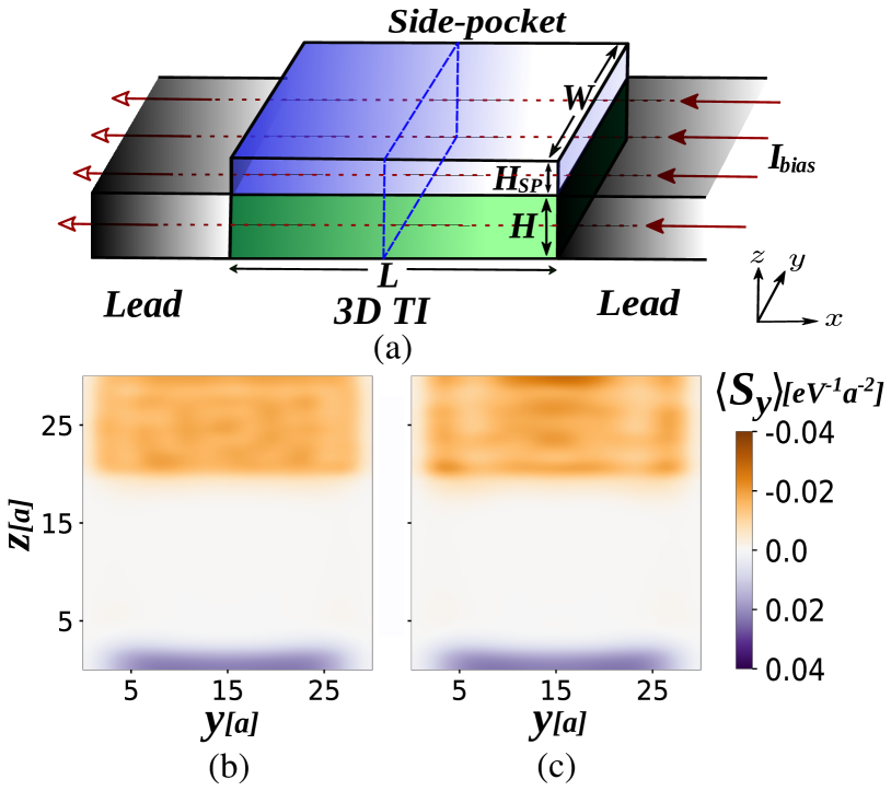
Spin extraction can take place at pockets that are attached to either surface of the 3DTI nanowire, see Fig. 4(a) and Fig. 5(a) for the geometry where the pocket is attached to the surface or the surface, respectively. The pockets are gated in order to tune them to a metallic state, while charge carriers can be either electron- or hole-like states, thus coupling only to the electron- or hole-like spin-momentum locked components of the 3DTI surface states. The gating is modeled by adding a corresponding on-site energy term in the tight-binding grid, while keeping the other parameters of the effective Hamiltonian unchanged.
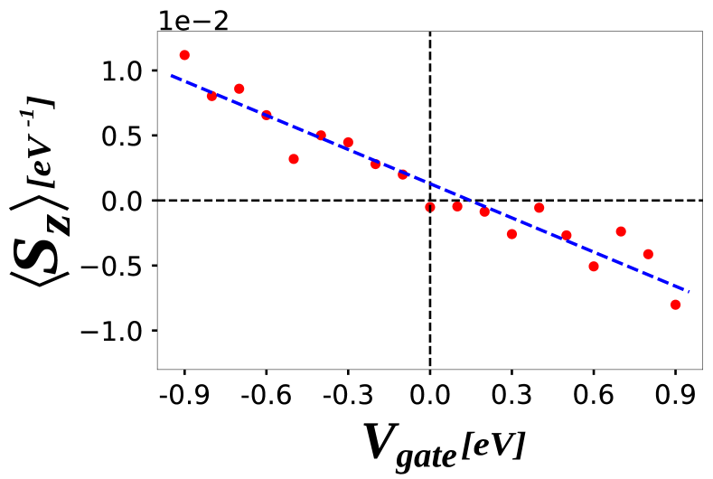
We perform tight-binding simulations and numerically calculate the current-induced spin polarization , (), averaging over 1000 disorder configurations for a nanowire with side pockets. Figs. 4(b), 4(c) and Figs. 5(b), 5(c) show the spatial profile of the spin polarization along a perpendicular cross-section for fixed doping values in hole and electron bands, respectively. Focusing on the top () surface, our simulations show all expected features: A substantial non-equilibrium spin accumulation can be extracted into the doped side pockets (Fig. 4). The extraction to the side () surface (Fig. 5), on the other hand, has non trivial features. We first note the somewhat surprising fact that even if the 3DTI surface has negligibly small spin accumulation, , the spin accumulation extracted into the side pocket is nonnegligible (see corresponding figures in Appendix C). Furthermore, the extracted spin polarization changes sign when the gate voltage is tuned so that the charge carriers change from electrons to holes as can be seen from Figs. 5(b) and 5(c). We find that the geometry of the contact does not play a crucial role as it does for a 2D electron gas with Rashba spin-orbit coupling: In that case wide contacts lead to reduced extraction adagideli2007extracting while for TIs wider contacts lead to enhanced extraction. In order to further study the spin-gate effect mentioned above, we plot the spin accumulation averaged over the side pocket, as a function of the gate voltage applied to the side pocket, in Fig. 6. We find that the spin accumulation depends linearly on the gate voltage and the sign of polarization changes by switching the side pocket polarity from hole- to electron-type.
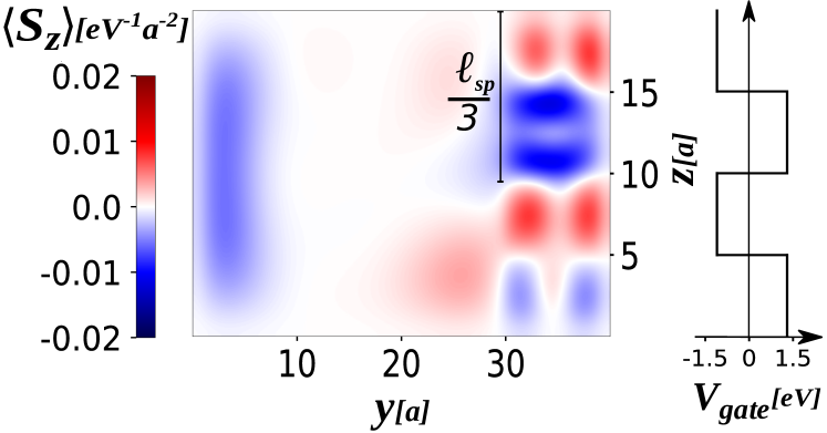
Finally we show that one can locally control the polarization direction of different parts of side pockets by local gating. In Fig. 7, we apply local gate profile where the electron puddles change into hole puddles within a region much smaller than the spin-precession length . We find that the spatial profile of the polarization of the extracted spin accumulation, closely follow the local gate potential. Thus, we show that it is possible to electrically control local spin polarization within length scales much smaller than the spin precession length.
IV Conclusions
In conclusion, we focus on the current-induced spins at the surfaces of 3DTIs and show how to extract these spins into topologically trivial materials commonly used in electronic devices. We find that unlike the corresponding effect in 2D electron gases with Rashba spin-orbit interaction, the mixing of the electron and hole degrees of freedom at the TI surface allows for additional methods for spin manipulation. In particular, we exposed a way to use electrical gate potentials to locally manipulate spins in regions smaller than the spin precession length. This opens up new possibilities for spin manipulation in spintronics devices.
Acknowledgements
A.A. thanks B. Pekerten and V. Sazgari for helpful conversations. This work was supported by Scientific and Technological Research Council of Turkey (TUBITAK) under Project Grant No. 114F163 and by the Deutsche Forschungsgemeinschaft (DFG, German Research Foundation) – Project-ID 314695032 – SFB 1277 (Subproject A07).
Appendix A Effective surface Hamiltonians and spin operators
Surface states in 3DTIs decay exponentially into the bulk and have energies in the bulk bandgap. We first consider a semi-infinite 3DTI system situated in () with a surface normal () pointing away from the bulk. By considering a vanishing boundary condition at the surface, eigenfunctions corresponding to these states can be written as
| (33) |
where the sign in the -direction corresponds to a system with a surface normal in the direction at . Here and is a spinor that is an eigenstate of the 3DTI Hamiltonian described in Eq. (20), corresponding to :
| (34) |
with energy dispersion to the lowest order of given by
| (35) |
where . Hence, the effective surface Hamiltonian as given in the text is obtained through projecting the 3DTI Hamiltonian in basis states given in Eq. (33) and using the spinor eigenstates stated in Eq. (34). To lowest order in and , this results in
| (36) |
which is introduced as Eq. (1) in the paper. The real spin operators for surface are formed by projecting the spin operators in the basis of bulk states, Eq. (21), onto the two surface states
| (37) |
which is stated as Eq. (2). The effective surface Hamiltonians and real spin operators corresponding to other surfaces can be calculated similarly.
Appendix B Mean free time estimation
We proceed with a Fermi’s Golden Rule estimation of the mean free path. The surface modes are 4-spinors with -dependent components shan2010 due to (pseudo)spin-momentum coupling. Such -dependence can lead to substantial differences between lifetime and transport time culcer2010 . In the case of uncorrelated disorder, however, the difference is only an -factor schwab2011 and thus irrelevant for our estimations. We thus work exclusively with band-bottom spinors. We consider a TI slab extended in and directions, having a length and a width along -direction and -direction, respectively, and a thickness along the -direction. We further assume white-noise disorder of the form . Therefore, using spinors stated in Eq. (34) leads to
| (38) |
where , and . We use Fermi’s Golden rule to derive the inverse mean free time and find
| (39) |
for surface states of a disordered 3DTI with semi-infinite boundary condition in -direction, i.e., . Based on Eq. (35), we have
| (40) |
Hence, the resulting total ensemble-averaged mean free time of surface states on the -surface reads
| (41) |
Similarly, for an energy dispersion, to the lowest order of , for -plane surface states,
| (42) |
we obtain the total ensemble-averaged inverse mean free time
| (43) |
where we approximate the Fermi velocity, , at this surface based on Eq. (42) since . Note that and are different values since the depth of the surface states into the bulk in different surfaces are not the same according to the parameters of the Hamiltonian.
Appendix C case
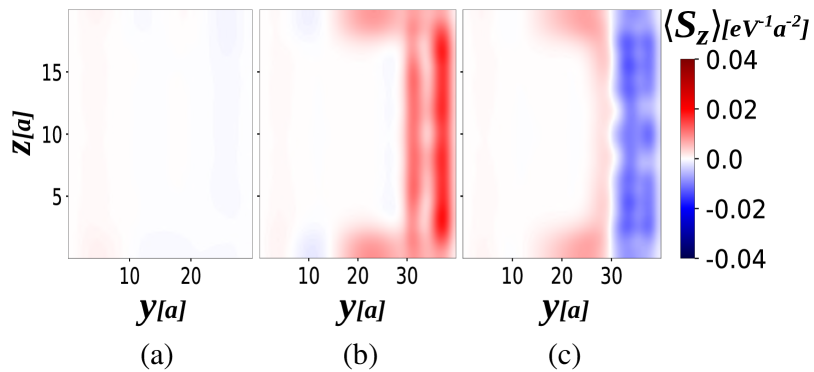
Here we provide figures for the case leading to . It is clearly seen that while there is negligible spin accumulation on the side of a 3DTI (Fig. 8(a)), spin extraction is nonnegligible in the side pocket and spin polarization can be switched via a gate potential (see Figs. 8(b) and 8(c)).
References
- (1) I. Žutić, J. Fabian, and S. D. Sarma, Rev. Mod. Phys. 76, 323 (2004).
- (2) D. C. Ralph and M. D. Stiles, J. Magn. Magn. Mater. 320, 1190 (2008).
- (3) S. A. Wolf, D. D. Awschalom, R. A. Buhrman, J. M. Daughton, S. von Molnar, M. L. Roukes, A. Y. Chtchelkanova, and D. M. Treger, Science 294, 1488 (2001).
- (4) K. Sato and H. Katayama-Yoshida, Semicond. Sci. Technol. 17, 367 (2002).
- (5) S. Datta and B. Das, Appl. Phys. Lett. 56, 665 (1990).
- (6) D. D. Awschalom, D. Loss, and N. Samarth, Semiconductor spintronics and quantum computation (Springer Science & Business Media, 2013).
- (7) Y. K. Kato, R. C. Myers, A. C. Gossard, and D. D. Awschalom, Science 306, 1910 (2004).
- (8) J. Schliemann, Rev. Mod. Phys. 89, 011001 (2017).
- (9) V. M. Edelstein, Solid State Commun. 73, 233 (1990).
- (10) J. Inoue, G. E. W. Bauer, and L. W. Molenkamp, Phys. Rev. B 67, 033104 (2003).
- (11) A. Y. Silov, P. A. Blajnov, J. H. Wolter, R. Hey, K. H. Ploog, and N. S. Averkiev, Appl. Phys. Lett. 85, 5929 (2004).
- (12) S. D. Ganichev, S. N. Danilov, P. Schneider, V. V. Bel’Kov, L. E. Golub, W. Wegscheider, D. Weiss, and W. Prettl, J. Magn. Magn. Mater. 300, 127 (2006).
- (13) M. I. D’yakonov and V. I. Perel, Sov. Phys. JETP 13, 467 (1971).
- (14) M. I. D’yakonov and V. I. Perel, Phys. Lett. A 35, 459 (1971).
- (15) J. E. Hirsch, Phys. Rev. Lett. 83, 1834 (1999).
- (16) M. Governale, F. Taddei, and R. Fazio, Phys. Rev. B 68, 155324 (2003).
- (17) A. G. Mal’shukov, C. S. Tang, C. S. Chu, and K. A. Chao, Phys. Rev. B 68, 233307 (2003).
- (18) S. Murakami, N. Nagosa, and S. C. Zhang, Phys. Rev. B 69, 235206 (2004).
- (19) M. Scheid, M. Kohda, Y. Kunihashi, K. Richter, and J. Nitta, Phys. Rev. Lett. 101, 266401 (2008).
- (20) A. G. Aronov and Y. B. Lyanda-Geller, JETP Lett. 50, 431 (1989).
- (21) E. Saitoh, M. Ueda, H. Miyajima, and G. Tatara, Appl. Phys. Lett. 88, 182509 (2006).
- (22) T. Kimura, Y. Otani, T. Sato, S. Takahashi, and S. Maekawa, Phys. Rev. Lett. 98, 156601 (2007).
- (23) K. Uchida, S. Takahashi, K. Harii, J. Ieda, W. Koshibae, K. Ando, S. Maekawa, and E. Saitoh, Nature 455, 778 (2008).
- (24) S. O. Valenzuela and M. Tinkham, Nature 442, 176 (2006).
- (25) T. Seki, Y. Hasegawa, S. Mitani, S. Takahashi, H. Imamura, S. Maekawa, J. Nitta, and K. Takanashi, Nat. Mater. 7, 125 (2008).
- (26) S. D. Ganichev, E. L. Ivchenko, V. V. Bel’kov, S. A. Tarasenko, M. Sollinger, D. Weiss, W. Wegscheider, and W. Prettl, Nature 417, 153 (2002).
- (27) J. C. Rojas Sánchez, L. Vila, G. Desfonds, S. Gambarelli, J. P. Attané, J. M. De Teresa, C. Magén, and A. Fert, Nat. Commun. 4, 2944 (2013).
- (28) İ. Adagideli, M. Scheid, M. Wimmer, G. E. W. Bauer, and K. Richter, New J. Phys. 9, 382 (2007).
- (29) I. Žutić, J. Fabian, and S. Das Sarma, Phys. Rev. Lett. 88, 066603 (2002).
- (30) K. Shen, G. Vignale, and R. Raimondi, Phys. Rev. Lett. 112, 096601 (2014).
- (31) F. Zhang, C. L. Kane, and E. J. Mele, Phys. Rev. B 86, 081303(R) (2012).
- (32) P. G. Silvestrov, P. W. Brouwer, and E. G. Mishchenko, Phys. Rev. B 86, 075302 (2012).
- (33) L. Brey and H. A. Fertig, Phys. Rev. B 89, 085305 (2014).
- (34) H. Zhang, C. Liu, X. Qi, X. Dai, Z. Fang, and S. Zhang, Nat. Phys. 5, 438 (2009).
- (35) Y. L. Chen, J. G. Analytis, J.-H. Chu, Z. K. Liu, S.-K. Mo, X. L. Qi, H. J. Zhang, D. H. Lu, X. Dai, Z. Fang, S. C. Zhang, I. R. Fisher, Z. Hussain, and Z.-X. Shen, Science 325, 178 (2009).
- (36) Y. Xia, D. Qian, D. Hsieh, L. Wray, A. Pal, H. Lin, A. Bansil, D. Grauer, Y. S. Hor, R. J. Cava, and M. Z. Hasan., Nat. Phys. 5, 398 (2009).
- (37) Z. Alpichshev, J. G. Analytis, J.-H. Chu, I. R. Fisher, Y. L. Chen, Z. X. Shen, A. Fang, and A. Kapitulnik, Phys. Rev. Lett. 104, 016401 (2010).
- (38) T. Zhang, P. Cheng, X. Chen, J.-F. Jia, X. Ma, K. He, L. Wang, H. Zhang, X. Dai, Z. Fang, X. Xie, and Q.-K Xue, Phys. Rev. Lett. 103, 266803 (2009).
- (39) P. Cheng, C. Song, T. Zhang, Y. Zhang, Y. Wang, J.-F. Jia, J. Wang, Y. Wang, B.-F. Zhu, X. Chen, X. Ma, K. He, L. Wang, X. Dai, Z. Fang, X. Xie, X.-L. Qi, C.-X. Liu, S.-C. Zhang, and Q.-K. Xue, Phys. Rev. Lett. 105, 076801 (2010).
- (40) T. Hanaguri, K. Igarashi, M. Kawamura, H. Takagi, and T. Sasagawa, Phys. Rev. B 82, 081305 (2010).
- (41) Z. Alpichshev, J. G. Analytis, J.-H. Chu, I. Fisher, and A. Kapitulnik, Phys. Rev. B 84, 041104 (2011).
- (42) D. Hsieh, Y. Xia, L. Wray, D. Qian, A. Pal, J. H. Dil, J. Osterwalder, F. Meier, G. Bihlmayer, C. L. Kane, Y. S. Hor, R. J. Cava, and M. Z. Hasan, Science 323, 919 (2009).
- (43) E. L. Ivchenko, Y. B. Lyanda-Geller, and G. E. Pikus, Sov. Phys. JETP 71, 550 (1990).
- (44) S. D. Ganichev, M. Trushin, and J. Schliemann, ArXive-prints (2016), arXiv:1606.02043 [cond-mat.mes-hall].
- (45) C. Gorini, A. M. Sheikhabadi, K. Shen, I. V. Tokatly, G. Vignale, and R. Raimondi, Phys. Rev. B 95, 205424 (2017).
- (46) Y. Ando and M. Shiraishi, J. Phys. Soc. Jpn. 86, 011001 (2017).
- (47) C.-X. Liu, X.-L. Qi, H. Zhang, X. Dai, Z. Fang, and S.-C. Zhang, Phys. Rev. B 82, 045122 (2010).
- (48) J. H. Bardarson, P. W. Brouwer, and J. E. Moore, Phys. Rev. Lett. 105, 156803 (2010).
- (49) J. Ziegler, R. Kozlovsky, C. Gorini, M.-H. Liu, S. Weishäupl, H. Maier, R. Fischer, D. A. Kozlov, Z. D. Kvon, N. Mikhailov, S. A. Dvoretsky, K. Richter, and D. Weiss, Phys. Rev. B 97, 035157 (2018).
- (50) C. W. Groth, M. Wimmer, A. R. Akhmerov, and X. Waintal, New J. Phys. 16, 063065 (2014).
- (51) M. D’yakonov and V. Perel, Sov. Phys. Solid State, 13, 3023 (1972).
- (52) A. A. Burkov and D. G. Hawthorn, Phys. Rev. Lett. 105, 066802 (2010).
- (53) P. Schwab, R. Raimondi, and C. Gorini, EPL 93, 67004 (2011).
- (54) W.-Y. Shan, H.-Z. Lu, and S.-Q. Shen, New J. Phys. 12, 043048 (2010).
- (55) D. Culcer, E. H. Hwang, T. D. Stanescu, and S. Das Sarma, Phys. Rev. B 82, 155457 (2010).