Tunable bandwidths and gaps in twisted double bilayer graphene system on the verge of correlations
Abstract
We use temperature-dependent resistivity in small-angle twisted double bilayer graphene to measure bandwidths and gaps of the bands. This electron-hole asymmetric system has one set of non-dispersing bands that splits into two flat bands with the electric field - distinct from the twisted bilayer system. With electric field, the gap between two emergent flat bands increases monotonically and bandwidth is tuned from 1 meV to 15 meV. These two flat bands with gap result in a series of thermally induced insulator to metal transitions - we use a model, at charge neutrality, to measure the bandwidth using only transport measurements. Having two flat bands with tunable gap and bandwidth offers an opportunity to probe the emergence of correlations.
The ability to tune the twist angle between two sheets of two-dimensional materials has enormously increased the scope of engineering superlattices Li et al. (2010); Wang et al. (2012); Cao et al. (2016). Following theoretical predictions Bistritzer and MacDonald (2011); Suárez Morell et al. (2010); Lopes dos Santos et al. (2012), some recent experiments have confirmed flat bands for twisted bilayer graphene system near a magic angle. In addition, for some parameter space, it hosts highly correlated states showing exotic phenomena including Mott insulator, superconductivity, and ferromagnetism Cao et al. (2018a, b); Kim et al. (2017); Sharpe et al. (2019); Lu et al. (2019). The ratio of electron-electron interaction strength and width of the electronic band is a key parameter determining the emergence of correlations. It is desirable to find additional knobs to tune the bandwidth Yankowitz et al. (2019); Chen et al. (2019a, b).
Twisted double bilayer graphene (TDBG) is also an interesting platform where one puts a copy of bilayer graphene on top of another one with a twist angle between them. The Bernal-stacked bilayer graphene has a unique band structure that changes upon applying perpendicular electric field as a bandgap opens up with increasing field Castro et al. (2007); Oostinga et al. (2008); Zhang et al. (2009); Castro Neto et al. (2009). The TDBG system inherits this tunability with the electric field and makes itself an interesting system with electrically tunable flat bands Chebrolu et al. (2019); Zhang et al. (2019); Koshino (2019); Lee et al. (2019); Choi and Choi (2019). However, there are only few experimental reports so far on this novel system where electric field tunable correlated insulating states and the realization of superconductivity have been demonstrated Shen et al. (2019); Liu et al. (2019); Cao et al. (2019); Burg et al. (2019). There is an urgent need to understand the single-particle band structure and this requires a detailed study of electron transport in small-angle TDBG system to understand bandgaps, bandwidths, and their tunability with the electric field.
In this work, we present a comprehensive study of temperature dependence of electronic transport in a twisted double bilayer graphene device with a twist angle of between the two sheets of bilayer graphene. This electron-hole asymmetric system has one set of low-energy non-dispersing bands separated from higher energy dispersing bands by moiré gaps at zero perpendicular electric field. As we increase electric field more, two clear trends emerge – firstly, after a finite electric field a bandgap opens up at the charge neutrality point giving rise to two flat bands; this differentiates it from twisted bilayer graphene, where the low energy bands always touch at the Dirac points Chebrolu et al. (2019); Koshino (2019). Secondly, further increase of electric field closes the moiré gaps gradually in an asymmetric manner for electron and hole side. By systematic measurement of gaps as a function of electric field we establish both these trends experimentally. We then focus on understanding the thermally induced insulator to metal transitions in the parameter space of electric field and charge density. We show that this physics can be understood using a simple model with two flat bands at a finite perpendicular electric field. Applying this simple double quantum well with flat band model Mandrus et al. (1995) we extract, using only transport measurements, the bandwidth tunable from meV to meV by increasing the electric displacement field strength, from V/nm to V/nm. The moiré gaps separating the flat bands from the dispersing higher bands are meV. The fact that the gaps and bandwidths are tunable with the electric field makes this system important for studying correlations.
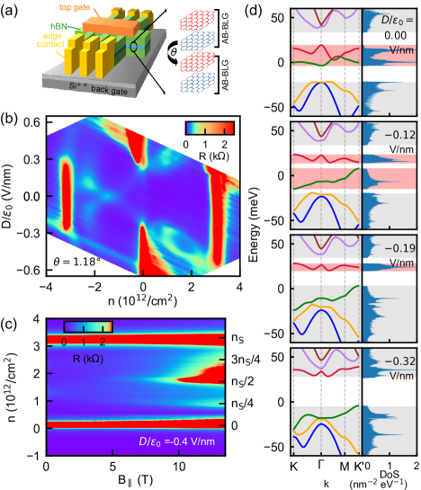
We now discuss the details of our experiment. As shown in the schematic in Fig. 1(a), the twisted double bilayer graphene is encapsulated by both top and bottom few layers thick hexagonal boron nitride Wang et al. (2013); Kim et al. (2016); Cao et al. (2016). For details of the fabrication process, see Section I in Supplemental Material sup . The metallic top gate and the Si++ back gate allow us independent control of both the carrier density and the perpendicular electric displacement field , given by the equations and , where and are the capacitance per unit area of the top and the back gate respectively, being the charge of an electron.
Figure 1(b) shows a color scale plot of the four-probe resistance, , as a function of and measured at a temperature of 1.5 K. Firstly, this TDBG device shows two pronounced peaks in resistance corresponding to the two moiré gaps at , where cm-2 is the required charge density to fill the first moiré band corresponding to a twist angle of . Another peak in resistance appears at the charge neutrality point (CNP) as the magnitude of is increased indicating gap opening with the electric field. This is also seen in simple bilayer graphene device Oostinga et al. (2008); Zhang et al. (2009). However, the resistance at the two moiré gaps decreases with increasing electric field, indicating gradual closing of these gaps. Secondly, as reported in some very recent works on TDBG Shen et al. (2019); Liu et al. (2019); Cao et al. (2019); Burg et al. (2019) there are several interesting features at specific parameter space, namely, a cross-like feature around zero electric field only on the hole side and two halo regions of high resistance present at the electric displacement field V/nm on the electron side. In this device, we do not observe fully formed insulating states at filling other than and at zero magnetic field. We intentionally use this system as we do not want any of the gaps to be enhanced due to correlations. However, Fig. 1(c) shows that with the in-plane magnetic field, gaps open up at , and for this device – suggesting that the system is on the verge of developing correlations. All of these observations indicate the existence of flat band physics and offer an opportunity to study the temperature dependence of transport properties in a flat band system. See Fig. S8 in Supplemental Material sup for data from another TDBG device with a twist angle that shows two moiré gaps at and gap opening at CNP, but no other features like the cross or the halo. This emphasizes the role of the flat bands in the device with twist angle.
From Fig. 1(b) it is evident that this system possesses a high degree of electron-hole asymmetry. While the asymmetric presence of above mentioned cross-like feature and the halo feature are such examples, the different closing sequence of two moiré gaps offers another one. Different theoretical aspects of twisted angle systems have been understood using a minimal model where one sets further neighbor hoppings across the bilayer, and , as well as the potential on dimer sites to be zero. However, to capture the electron-hole asymmetry we use an e-h asymmetric model with meV, meV, and meV (see Section II in Supplemental Material sup for details). In Fig. 1(d) (left panels) we calculate the band structures of TDBG for a twist angle of for four different values of electric fields based on this e-h asymmetric model. The corresponding density of states is plotted in the right panels of Fig. 1(d), which depicts various gaps in agreement with those seen from the resistance variation in Fig. 1(b).
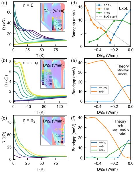
We now probe the electron-hole asymmetry in detail by extracting the values of different gaps with varying electric field. Figures 2(a-c) show the variation of resistance as a function of temperature for different electric fields at , , and respectively. We extract gaps, , by fitting at the regime where the resistance decreases exponentially with the temperature. See Section III in Supplemental Material sup for details of the fits. The vs. curves show deviation from the Arrhenius nature at low temperature. In particular, we see a shoulder like variation, which is most prominent for with stronger than V/nm (see Section IV in Supplemental Material sup for details). In Fig. 2(d) we plot extracted gaps as a function of the perpendicular electric field. Consistent with the band picture we presented in the earlier section, the gap at the charge neutrality point increases with the electric field, while the gaps for decrease. An interesting observation is that the gap at CNP starts opening only after a finite electric displacement field of V/nm, in contrast to bilayer graphene where the gap opens up as soon as any non-zero electric field is applied (see Fig. S9 in Supplemental Material sup ). A similar analysis for the device with a twist angle shows non-monotonic behavior of gap with the electric field as the CNP gap closes and reopens with the increasing electric field (see Fig. S8 in Supplemental Material sup ). In Fig. 2(e) and 2(f), we present the calculated gaps based on the minimal model and the e-h asymmetric model respectively. The opening of the CNP gap only after V/nm shows the inadequacy of the minimal model, which indicates a finite gap at any non zero electric field. However, the e-h asymmetric model captures the correct trend of the variation of gaps with the electric field for all three different values of , though overestimating the gaps quantitatively.
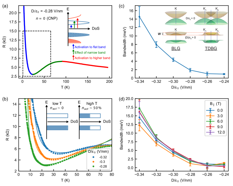
In Fig. 3(a) we plot a typical resistance vs. temperature curve at for V/nm when the Fermi energy lies in the CNP gap between two flat bands separated from higher band by moiré gaps as shown in the inset of Fig. 3(a). Clearly, there are three distinct temperature regions governed by three different energy scales – the CNP gap, the flat band width and the separation of higher-energy bands from the Fermi energy. While resistance shows insulating behavior at low temperature (blue) due to activation of carriers to flat band, at high temperature (red) this is governed by the activation to higher dispersing band. The thermal activation of charge carriers to higher dispersing bands is also captured by the metal to insulator transition for the states where the chemical potential lies within the flat band, not just at CNP (see Section VII in Supplemental Material sup for details) Polshyn et al. (2019).
However, there is a mid-range temperature regime (green) where resistance increases with temperature. We now closely examine the temperature regime within the dashed box in Fig. 3(a) and illustrate how the existence of two flat bands separated by a narrow gap can account for this crossover. We employ a simple model, as depicted in the inset of Fig. 3(b) where we consider two narrow bands with bandwidth of having the constant density of states with a narrow gap of between them. Here is the number of electrons to fill one such band. We note, this model is most appropriately valid before the closure of the moiré gap. As the temperature is increased, the carriers are activated in the narrow bands governed by the Fermi-Dirac distribution, which results in the usual decrease in resistance. However, due to the small energy scales set by and , the number of activated carriers quickly saturates to the value one would get at a very high temperature, (see Section VI in Supplemental Material sup ). On the other hand, the mobility keeps on decreasing with increasing temperature and takes over the increase in activated carrier density to show a metal-like increase in resistance.
To quantitatively understand this insulator to metal transition seen in Fig. 3(b), we assume a phonon-scattering dominated temperature variation of the mobility of the form . We calculate the conductance using the relation . Here is the charge of electron and is the number of activated carriers given by with being the Fermi-Dirac function. We then fit the resultant expression of the conductivity with three fitting parameters, namely, the bandwidth , the bandgap , and the overall factor , to the experimental data. Few such fitting curves are overlayed with the experimental data in Fig. 3(b). While it deviates at high temperature due to carrier activation to the higher band, the low temperature deviation can be understood since the simple picture of the mobility decreasing with temperature does not hold good.
In Fig. 3(c), we plot the extracted bandwidths as a function of the electric field. The bandwidth has a clear trend of increasing with the electric field. This reasonably agrees with the results discussed in N. R. Chebrolu et al. Chebrolu et al. (2019). The bandwidth has a typical value meV for mid-range of the electric field where the halo features appear on the electron side.
The origin of the electric field tunability of the bandwidth is subject of detail theoretical and numerical calculation Chebrolu et al. (2019). However, a simple picture is depicted in the inset of Fig. 3(c) considering the tunability of underlying BLG band structure. Upon applying electric field low energy part of quadratic bands in BLG forms a “Mexican hat" structure with local maxima and minima around points in the Brillouin zone Castro et al. (2007); Castro Neto et al. (2009). The depth of the Mexican hat scales approximately as the cube of the electric field. Small angle twist of two copies of BLG in TDBG effectively hybridizes such adjacent cones and the bandwidth of the low energy flat band inherits the electric field dependence of the depth of the Mexican hat in BLG. The tunability of this energy scale may be enhanced in TDBG from that of BLG due to additional hopping terms and modified effective mass.
Finally, we study the effect of in-plane magnetic field on the bandwidth, motivated by its profound role to enhance correlated gaps as already seen in Fig. 1(c). In Fig. 3(d) we plot the variation of bandwidth with electric field for different magnitude of in-plane magnetic field. The overlapping error bars suggest there is no clear trend implying that the bandwidth is not substantially tuned with in-plane magnetic field.
We find TDBG to be a highly tunable system with moiré gaps that can be closed with increasing electric field while the flat bands split into two; eventually, the two narrow flat bands merge with the higher dispersing bands. A plethora of novel phenomena have been identified to be originating from the underlying flat bands in twisted graphene system, without directly quantifying the flatness of the bands using transport. In strongly correlated systems, the bandwidths and gaps can be enhanced because of interactions. Our choice of a weakly interacting system and subsequent analysis provide a route to quantitatively establish tunability of bandwidth with electric field in flat band systems for the first time.
We thank Allan MacDonald, Senthil Todadri, Sreejith GJ, Priyanka Mohan and Biswajit Datta for helpful discussions. We acknowledge Nanomission grant SR/NM/NS-45/2016 and Department of Atomic Energy of Government of India for support. U. G. and R. S. thanks the computational facility at Department of Theoretical Physics, TIFR, Mumbai. Preparation of hBN single crystals is supported by the Elemental Strategy Initiative conducted by the MEXT, Japan and JSPS KAKENHI Grant Number JP15K21722.
References
- Li et al. (2010) G. Li, A. Luican, J. M. B. Lopes dos Santos, A. H. Castro Neto, A. Reina, J. Kong, and E. Y. Andrei, Nature Physics 6, 109 (2010).
- Wang et al. (2012) Z. F. Wang, F. Liu, and M. Y. Chou, Nano Letters 12, 3833 (2012).
- Cao et al. (2016) Y. Cao, J. Y. Luo, V. Fatemi, S. Fang, J. D. Sanchez-Yamagishi, K. Watanabe, T. Taniguchi, E. Kaxiras, and P. Jarillo-Herrero, Physical Review Letters 117, 116804 (2016).
- Bistritzer and MacDonald (2011) R. Bistritzer and A. H. MacDonald, Proceedings of the National Academy of Sciences 108, 12233 (2011).
- Suárez Morell et al. (2010) E. Suárez Morell, J. D. Correa, P. Vargas, M. Pacheco, and Z. Barticevic, Physical Review B 82, 121407 (2010).
- Lopes dos Santos et al. (2012) J. M. B. Lopes dos Santos, N. M. R. Peres, and A. H. Castro Neto, Physical Review B 86, 155449 (2012).
- Cao et al. (2018a) Y. Cao, V. Fatemi, A. Demir, S. Fang, S. L. Tomarken, J. Y. Luo, J. D. Sanchez-Yamagishi, K. Watanabe, T. Taniguchi, E. Kaxiras, R. C. Ashoori, and P. Jarillo-Herrero, Nature 556, 80 (2018a).
- Cao et al. (2018b) Y. Cao, V. Fatemi, S. Fang, K. Watanabe, T. Taniguchi, E. Kaxiras, and P. Jarillo-Herrero, Nature 556, 43 (2018b).
- Kim et al. (2017) K. Kim, A. DaSilva, S. Huang, B. Fallahazad, S. Larentis, T. Taniguchi, K. Watanabe, B. J. LeRoy, A. H. MacDonald, and E. Tutuc, Proceedings of the National Academy of Sciences 114, 3364 (2017).
- Sharpe et al. (2019) A. L. Sharpe, E. J. Fox, A. W. Barnard, J. Finney, K. Watanabe, T. Taniguchi, M. A. Kastner, and D. Goldhaber-Gordon, Science 365, 605 (2019).
- Lu et al. (2019) X. Lu, P. Stepanov, W. Yang, M. Xie, M. A. Aamir, I. Das, C. Urgell, K. Watanabe, T. Taniguchi, G. Zhang, A. Bachtold, A. H. MacDonald, and D. K. Efetov, Nature 574, 653 (2019).
- Yankowitz et al. (2019) M. Yankowitz, S. Chen, H. Polshyn, Y. Zhang, K. Watanabe, T. Taniguchi, D. Graf, A. F. Young, and C. R. Dean, Science 363, 1059 (2019).
- Chen et al. (2019a) G. Chen, L. Jiang, S. Wu, B. Lyu, H. Li, B. L. Chittari, K. Watanabe, T. Taniguchi, Z. Shi, J. Jung, Y. Zhang, and F. Wang, Nature Physics 15, 237 (2019a).
- Chen et al. (2019b) G. Chen, A. L. Sharpe, P. Gallagher, I. T. Rosen, E. J. Fox, L. Jiang, B. Lyu, H. Li, K. Watanabe, T. Taniguchi, J. Jung, Z. Shi, D. Goldhaber-Gordon, Y. Zhang, and F. Wang, Nature 572, 215 (2019b).
- Castro et al. (2007) E. V. Castro, K. S. Novoselov, S. V. Morozov, N. M. R. Peres, J. M. B. L. dos Santos, J. Nilsson, F. Guinea, A. K. Geim, and A. H. C. Neto, Physical Review Letters 99, 216802 (2007).
- Oostinga et al. (2008) J. B. Oostinga, H. B. Heersche, X. Liu, A. F. Morpurgo, and L. M. K. Vandersypen, Nature Materials 7, 151 (2008).
- Zhang et al. (2009) Y. Zhang, T.-T. Tang, C. Girit, Z. Hao, M. C. Martin, A. Zettl, M. F. Crommie, Y. R. Shen, and F. Wang, Nature 459, 820 (2009).
- Castro Neto et al. (2009) A. H. Castro Neto, F. Guinea, N. M. R. Peres, K. S. Novoselov, and A. K. Geim, Reviews of Modern Physics 81, 109 (2009).
- Chebrolu et al. (2019) N. R. Chebrolu, B. L. Chittari, and J. Jung, Physical Review B 99 (2019), 10.1103/PhysRevB.99.235417.
- Zhang et al. (2019) Y.-H. Zhang, D. Mao, Y. Cao, P. Jarillo-Herrero, and T. Senthil, Physical Review B 99, 075127 (2019).
- Koshino (2019) M. Koshino, Physical Review B 99, 235406 (2019).
- Lee et al. (2019) J. Y. Lee, E. Khalaf, S. Liu, X. Liu, Z. Hao, P. Kim, and A. Vishwanath, Nature Communications 10, 1 (2019).
- Choi and Choi (2019) Y. W. Choi and H. J. Choi, Physical Review B 100 (2019), 10.1103/PhysRevB.100.201402.
- Shen et al. (2019) C. Shen, N. Li, S. Wang, Y. Zhao, J. Tang, J. Liu, J. Tian, Y. Chu, K. Watanabe, T. Taniguchi, R. Yang, Z. Y. Meng, D. Shi, and G. Zhang, arXiv:1903.06952 [cond-mat] (2019), arXiv:1903.06952 [cond-mat] .
- Liu et al. (2019) X. Liu, Z. Hao, E. Khalaf, J. Y. Lee, K. Watanabe, T. Taniguchi, A. Vishwanath, and P. Kim, arXiv:1903.08130 [cond-mat] (2019), arXiv:1903.08130 [cond-mat] .
- Cao et al. (2019) Y. Cao, D. Rodan-Legrain, O. Rubies-Bigorda, J. M. Park, K. Watanabe, T. Taniguchi, and P. Jarillo-Herrero, arXiv:1903.08596 [cond-mat] (2019), arXiv:1903.08596 [cond-mat] .
- Burg et al. (2019) G. W. Burg, J. Zhu, T. Taniguchi, K. Watanabe, A. H. MacDonald, and E. Tutuc, Physical Review Letters 123, 197702 (2019).
- Mandrus et al. (1995) D. Mandrus, J. L. Sarrao, A. Migliori, J. D. Thompson, and Z. Fisk, Physical Review B 51, 4763 (1995).
- Wang et al. (2013) L. Wang, I. Meric, P. Y. Huang, Q. Gao, Y. Gao, H. Tran, T. Taniguchi, K. Watanabe, L. M. Campos, D. A. Muller, J. Guo, P. Kim, J. Hone, K. L. Shepard, and C. R. Dean, Science 342, 614 (2013).
- Kim et al. (2016) K. Kim, M. Yankowitz, B. Fallahazad, S. Kang, H. C. P. Movva, S. Huang, S. Larentis, C. M. Corbet, T. Taniguchi, K. Watanabe, S. K. Banerjee, B. J. LeRoy, and E. Tutuc, Nano Letters 16, 1989 (2016).
- (31) See Supplemental Material for experimental methods, theoretical calculation and additional data.
- Polshyn et al. (2019) H. Polshyn, M. Yankowitz, S. Chen, Y. Zhang, K. Watanabe, T. Taniguchi, C. R. Dean, and A. F. Young, Nature Physics , 1 (2019).