Observation of Protected Photonic Edge States Induced By
Real-Space Topological Lattice Defects
Abstract
Topological defects (TDs) in crystal lattices are elementary lattice imperfections that cannot be removed by local perturbations, due to their real space topology. We show that adding TDs into a valley photonic crystal generates a lattice disclination that acts like a domain wall and hosts topological edge states. The disclination functions as a freeform waveguide connecting a pair of TDs of opposite topological charge. This interplay between the real-space topology of lattice defects and band topology provides a novel scheme to implement large-scale photonic structures with complex arrangements of robust topological waveguides and resonators.
I Introduction
The field of topological photonics Ozawa et al. (2019), which has emerged over the past decade, seeks to use ideas from topological band theory Bansil et al. (2016) to realize photonic modes that are protected against various forms of disorder. Possible applications for this new class of photonic devices are still being explored, and may include robust waveguides and delay lines Hafezi et al. (2011); Wang et al. (2008, 2009); Dong et al. (2017); Shalaev et al. (2019), frequency converters Hadad et al. (2018); Wang et al. (2019), and lasers St-Jean et al. (2017); Zhao et al. (2018); Parto et al. (2018); Ota et al. (2018); Bandres et al. (2018); Harari et al. (2018). A key challenge to finding practical uses for topological photonic modes is that they are typically only robust against specific types of disorder. For example, photonic crystals based on valley Hall insulators Ma and Shvets (2016); Dong et al. (2017); Gao et al. (2017); He et al. (2019) and topological crystalline insulators Wu and Hu (2015); Barik et al. (2018) have been intensively studied, particularly in the nanophotonic regime, because they can be implemented using ordinary dielectric or metallic materials. Since their topological features are tied to the presence of an underlying lattice symmetry, their topological edge states are only protected against backscattering in certain configurations (e.g., 120∘ bends in valley photonic crystal edges Ma and Shvets (2016)), whereas other configurations can induce backscattering and mode localization.
Topological defects (TDs) in crystal lattices are elementary lattice imperfections that cannot be removed by local perturbations, due to their real space topology Mermin (1979). In condensed matter systems, TDs are responsible for many interesting effects, including acting as seeds of disorder in the melting of two-dimensional (2D) solids Kosterlitz (2017). Honeycomb lattices, such as graphene, host a particularly notable class of TDs consisting of five- and seven-membered rings, which act upon 2D Dirac cone states like singular matrix-valued gauge fields carrying magnetic flux González et al. (1993); Lammert and Crespi (2000); Vozmediano et al. (2010); Kotakoski et al. (2011); de Souza et al. (2014). Experimental evidence of these electronic features has proven difficult to obtain, due in part to challenges in sample preparation Yazyev and Louie (2010); Kotakoski et al. (2011); Lahiri et al. (2010); Huang et al. (2011); Warner et al. (2012). Such difficulties can be overcome by photonic structures, which can realize many phenomena that are hard to observe in condensed matter settings. For example, photonic honeycomb lattices (“photonic graphene”) have been shown to exhibit unconventional edge states that are difficult to stabilize in real graphene Plotnik et al. (2014). The aforementioned physical effects of TDs, however, have yet to be explored on photonic platforms.
Here, we present a theoretical and experimental study of topologically protected waveguiding aided by TDs in valley photonic crystals (VPCs). In honeycomb lattices with broken sublattice symmetry, TDs are the termination points of disclinations—string-like lattice defects—that cannot be gauged away Rüegg and Lin (2013); de Souza et al. (2014). We show that these disclinations are locally equivalent to domain walls of Valley Hall insulators Ma and Shvets (2016); Dong et al. (2017); Gao et al. (2017) and thus function as robust topological edge state waveguides Ozawa et al. (2019).
TDs supply a novel and interesting relationship between topological features and edge states that is completely different from the usual bulk-edge correspondence principle. They carry topological charges in real space (negative for pentagonal TDs, positive for heptagonal TDs) that stem from the configuration of the lattice instead of bandstructure features defined in momentum space. Positive and negative TDs are joined pairwise by disclinations hosting edge states; but unlike standard VPC domain walls, one can go smoothly from one domain to the other by encircling a TD without crossing the disclination. This feature requires the presence of TDs and does not occur in perfectly crystalline VPCs. The disclinations can follow curved paths and are not restricted to any global axes Ma and Shvets (2016); Gao et al. (2017). They are also not limited to forming loops or ending at external boundaries, and can form open arcs (bounded by the TDs) that act as one-dimensional (1D) Fabry-Pérot resonators based on counterpropagating topological edge states.
Previous research has shown that amorphous photonic structures (which possess short-range positional order without long-range order) can exhibit isotropic photonic band gaps, and can be inscribed with freeform curved waveguides Miyazaki et al. (2003); Edagawa et al. (2008); Florescu et al. (2009); Yang et al. (2010); Imagawa et al. (2010); Man et al. (2013); Florescu et al. (2013). A key limitation of such waveguides is that, as 1D disordered transport channels, they are highly susceptible to Anderson localization Kramer and MacKinnon (1993), making it necessary to perform structural fine-tuning to optimize the localization lengths of the waveguide modes Florescu et al. (2013). We show that the present disclination-based waveguides display much greater resistance against Anderson localization, without structural fine-tuning, thanks to their connection to Valley Hall edge states Ozawa et al. (2019); Ma and Shvets (2016). Smooth curves in the waveguide act like large-scale impurities, while sharper bends can be implemented using local 120∘ bends, both of which induce negligible inter-valley scattering and hence preserve the topological protection of the edge states Ma and Shvets (2016). Unlike earlier demonstrations of topological waveguiding in amorphous or quasicrystalline lattices Bandres et al. (2016); Mitchell et al. (2018), the present VPC-based design does not require breaking time-reversal symmetry.
II Topological Defects in Photonic Lattices
Consider the honeycomb lattice shown in Fig. 1(a). The red and blue circles represent the and sublattices, which have on-site masses . As shown in Fig. 1(b), by deleting the sector marked by the dashed lines and reattaching the seams, we can generate a pentagonal TD, which features a five-membered ring González et al. (1993). Likewise, inserting an additional sector yields a heptagonal TD, as shown in Fig. 1(c). Each topological defect is attached to a string disclination, marked by the gray dashes in Fig. 1(b)–(c). On opposite sides of the disclination, sites of the same sublattice are nearest neighbors, whereas all other nearest neighbor pairs occupy different sublattices.
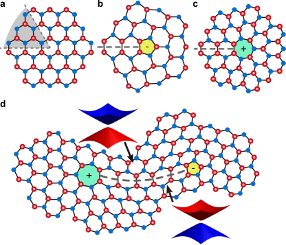
When , the disclination is ficticious in the sense that it can be moved around freely, so long as it terminates at the topological defect, by adjusting the assignment of sites to the and sublattices. In the continuum limit, the states of the honeycomb lattice are described by a pair of Dirac cones. The introduction of a TD imposes a disclination associated with a nontrivial boundary condition for the Dirac cone states, which several authors have shown can be gauged away—i.e., the boundary condition can be transformed into a regular continuity condition via the introduction of a matrix-valued gauge field González et al. (1993); Lammert and Crespi (2000, 2004); Rüegg and Lin (2013).
For , the case we are primarily interested in, the disclination is physical and cannot be gauged away Rüegg and Lin (2013). The disclination consists of neighboring sites of the same sublattice, which is strongly reminiscent of valley Hall domain walls and hence indicates that valley Hall-like topological edge states should exist along the disclination. (But unlike a valley Hall domain wall, which is only allowed to form a loop or terminate at exterior lattice edges, the disclination can terminate at a point in the bulk, at the position of the topological defect.) In Appendix A, we present a theoretical analysis of the Dirac cone states in the continuum limit, showing that they indeed experience a valley Hall-like domain wall at the disclination—i.e., each valley sees a change in sign of the Dirac mass across the disclination.
To confirm the existence of edge states bound to disclinations, we performed experiments on VPC with dielectric pillars. The pillars are sandwiched between parallel metal plates, and the experiments are performed in the microwave regime. Details of the setup are given in Appendix B.
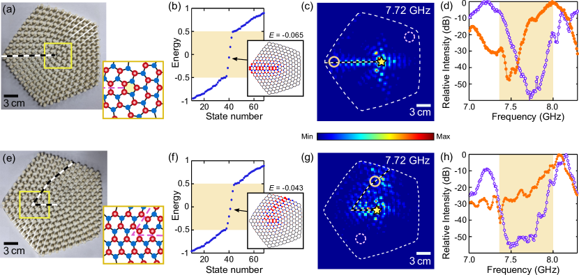
In the first set of experiments, we designed and fabricated VPC with a single pentagonal TD at the center, as shown in Fig. 2(a) and (e). To create these patterns, we start with a or sector, populate it with an unoptimized triangular lattice, and close-pack those lattice sites using the molecular dynamics simulator LAMMPS Plimpton (1995). The other sectors are then determined by five- or seven-fold rotational symmetry, yielding a lattice centered on a TD. The honeycomb-like dual lattice is generated by interpreting the triangular lattice sites as the incenters of the honeycomb motifs Mansha et al. (2016).
The lattice sites are “colored” by assigning them to sublattice or , corresponding to pillar radius or respectively (see Appendix B). Wherever possible, neighboring sites are assigned to opposite sublattices, but this cannot be achieved everywhere: there is always a disclination—a string of lattice edges joining neighboring sites of the same sublattice—emanating from the topological defect. By changing the lattice coloring, we can vary the path of the disclination, including making it turn sharp corners. The top and bottom rows of Fig. 2 show results for two different disclination choices.
To study the qualitative features of these lattice configurations, we calculate the energy spectrum of the corresponding tight-binding models. Fig. 2(b) and (f) show results for the two different disclinations, with nearest neighbor hopping and on-site mass and for the and sublattices. For these parameters (which are chosen for convenience, not to fit experiments), the equivalent honeycomb lattice has a bulk band gap at . The numerical results show that the lattices with a TD have eigenstates in the band gap. As shown in the insets of Fig. 2(b) and (f), the states are localized to the disclination, similar to domain wall states of valley Hall insulators.
Fig. 2(c) and (g) plot the experimentally measured intensity profiles for transverse mangetic (TM) waves emitted by a dipole source placed at the TD (oriented perpendicular to the plane). The excitation frequency of lies within the bulk band gap of an equivalent VPCl with the same choice of parameters (–; see Appendix B). We observe that the light emitted by the dipole is guided along the disclination, including around a sharp corner in the case of Fig. 2(g). In Fig. 2(d) and (h), we plot the experimentally measured frequency dependence of the local field intensities averaged over different regions of the lattice. In the frequency range of the bulk band gap, there is a clear intensity dip when the sampling region lies away from the disclination, but no dip when the sampling region lies over the disclination.
For comparison, we also investigated a “photonic graphene” lattice in which every pillar has the same radius (i.e., sublattice symmetry is unbroken). According to previous theoretical studies,TDs in such lattices should not create localized resonances Lammert and Crespi (2000, 2004); Rüegg and Lin (2013), and due to the lack of sublattice symmetry breaking there is no disclination on which edge states can appear. This is consistent with our experimental findings, which are summarized in Appendix C.
III Waveguiding with topological and non-topological defects
The lattices studied in the previous section have a relatively simple arrangement, with five- or seven-fold rotational symmetry around a central TD. In this section, we study more complex VPC with TDs hosting freeform topological waveguides.
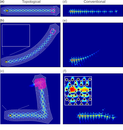
To investigate this empirically, we implemented several large-scale VPCs hosting topological and non-topological waveguides. As shown in Fig. 3, each waveguide forms an open arc following a straight path, a curved path, or a curved path containing a sharp bend. Each topological waveguide runs along a disclination connecting a pentagonal and a heptagonal TD; the lattice generation procedure is similar to the one previously described (i.e., generation of an unoptimized lattice containing the desired topological defects, close packing, conversion to a dual honeycomb-like lattice, and lattice coloring). The parameters of the VPCs are the same as before (see Appendix B).
Figure 3(a)–(c) shows simulated field distributions produced by a dipole source placed at one TD. For all three configurations, we observe a roughly uniform intensity distribution along the entire open arc of the waveguide. The waveguides can thus be regarded as 1D Fabry-Pérot-like optical cavities, with the topological defects serving as end mirrors (i.e., the waveguide modes experience complete inter-valley scattering and back-reflection at these points). The uniformity of the intensity distribution indicates that there is negligible Anderson localization, as well as negligible backscattering at the sharp bend in the case of Fig. 3(c).
For comparison, we also implemented a set of conventional (non-topological) waveguides in similar photonic lattices. The lattices have the same bulk parameters as before (i.e., the same pillar radii and mean inter-pillar spacings), but lack topological defects. The waveguides do not run along disclinations, but are instead formed by the selective removal of pillars along a desired route. In a perfectly crystalline lattice, photonic bandstructure calculations show that the pillar removal procedure creates a band of defect modes in the frequency range –, close to the center of the bulk band gap (these are not topological modes, so they do not span the gap). Simulations show that the defect modes transmit efficiently when the waveguide follows a straight line [Fig. 3(d)], but suffer from localization when the route is curved [Fig. 3(e)]. They are also unable to guide light efficiently around sharp corners [Fig. 3(f)].
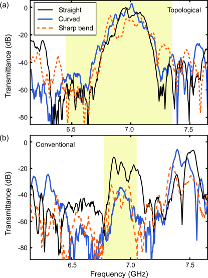
We experimentally implemented these six photonic structures, and measured the transmission between the two TDs of the waveguides. The results are shown in Fig. 4. For the topological waveguides, the three routes (straight, curved, and sharply bent) all produce similar transmission characteristics at frequencies close to the center of the bulk band gap. The operating frequency bandwidth appears to be somewhat narrower than the full width of the bulk band gap as predicted from simulations, possibly due to intrinsic losses in the ceramic material as well as input and output impedances. For the conventional waveguides, the bent and curved routes transmit markedly less efficiently, with transmittances around lower than the straight conventional waveguide, and – lower than the topological waveguides.
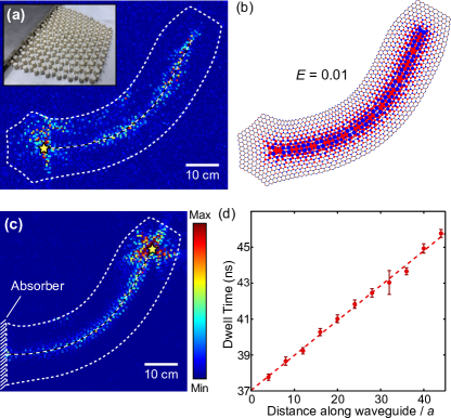
We also performed field-mapping experiments on a curved topological waveguide [Fig. 5(a)–(b)]. As shown in Fig. 5(a), strong field intensities are observed along the entire length of the waveguide, consistent with the behavior in simulations (Fig. 3). In these experiments, there is a air gap between the moving top plate and the pillars, which causes a small frequency shift in the band structure. The shifted bulk band gap is estimated to be – (see Appendix B).
To further probe the nature of the waveguide modes, we studied another sample in which the curved topological waveguide terminates at an external boundary lined with microwave-absorbing foam, rather than a TD. Due to the suppressed back-reflection, this waveguide should only contain waves traveling in one direction, away from the source. The experimental field intensity map is shown in Fig. 5(c). We then measured the dwell time at different positions along the waveguide Cheng et al. (2016). The dwell time is defined as , where is the phase of the measured field and is the angular frequency. To estimate the derivative, we approximate the derivative using a finite frequency spacing . For each data point, we use a total of 61 dwell time estimates, centered around the frequency close to the center of the gap. The resulting mean (and standard error of the mean) are plotted in Fig. 5(d). We find that the dwell time scales linearly with distance (arc length) along the curved waveguide, consistent with the expectation that the edge states propagate ballistically.
IV Discussion
We have demonstrated that TDs-induced disclinations in VPCs enable a novel scheme for implementing complex large-scale photonic structures, by placing TDs at the desired end-points and adjusting the disclinations to follow the desired waveguide routes. The waveguides enjoy much greater resistance to backscattering than freeform waveguides in amorphous photonic lattices designed without topological principles Florescu et al. (2013); Man et al. (2013). Though originally implemented at microwave frequencies, our all-dielectric design can be straightforwardly scaled to higher frequencies, as demonstrated by the recent implementation of VPCs in the optical regime Shalaev et al. (2019). From a fundamental point of view, we have demonstrated a new interplay between the real-space topology of a lattice and the momentum-space topology of Bloch wavefunctions, which is different from the previously-known topological bulk-edge correspondence principle. This phenomenon makes the presence of TDs in 2D honeycomb lattices, previously a relatively subtle effect, now easily observable. In future work, it will be interesting to investigate TDs and disclinations in other types of topological photonic lattices, such as higher-order topological insulators Noh et al. (2018), as well as experimentally accessing other phenomena associated with TDs such as anomalous Aharanov-Bohm effects and localized zero modes González et al. (1993); Lammert and Crespi (2000, 2004); Sitenko and Vlasii (2007); Cortijo and Vozmediano (2007); Rüegg and Lin (2013); de Souza et al. (2014); Jeong et al. (2008); Vozmediano et al. (2010); Yazyev and Louie (2010); Kotakoski et al. (2011); Wei et al. (2012).
Appendix A Effects of Topological Lattice Defects on Dirac Cone States
In this Appendix, we describe the continuum limit for 2D honeycomb lattices containing topological defects, and the role of the disclinations attached to those defects.
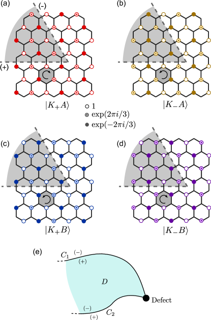
We begin with a perfect honeycomb lattice without topological defects. Let denote a set of Dirac point states, where is the valley index and is the sublattice index. As shown in Fig. 6(a)–(d), these states can be defined so that the amplitudes on the lattice sites are , where , with each Dirac point state occupying a single sublattice, or . Note that the two states in each valley have opposite chirality. The basis wavefunctions, , obey the time-reversal relation
| (1) |
Microscopic wavefunctions can be expressed as
| (2) |
where the ’s are slowly-varying envelope functions. These form a four-component spinor field that is governed by a 2D Dirac equation , where
| (3) |
Here is the Dirac velocity, () denote valley (sublattice) Pauli matrices, is the sublattice detuning, and is the eigenfrequency or eigenenergy.
Next, we introduce a topological defect, e.g. by deleting the sector marked in gray in Fig. 6(a)–(d). We can use the same pattern of site amplitudes as before to define a set of basis functions for the altered lattice Lammert and Crespi (2000, 2004). Then Eq. (2) still applies, but the Dirac equation governing may be changed. There are two distinct modifications to account for: (i) the lattice is spatially distorted in order to join up the seams of the deleted (or inserted) sector, which alters the effective Hamiltonian; (ii) the wavefunctions must satisfy some boundary condition along the disclination.
We consider these two issues in turn. The distortion of the lattice can be modeled as a local frame rotation, which manifests in the effective Hamiltonian as follows:
| (4) |
where is a position-dependent frame rotation angle. The lattice strain may also introduce other changes to , such as additional synthetic gauge fields, which we shall neglect. The frame rotation angle is discontinous across the disclination, with
| (5) |
where applies to a pentagonal (heptagonal) defect.
Next, we determine the boundary conditions along the disclination. An examination of Fig. 6(a)–(d) indicates that
where the and superscripts respectively indicate the clockwise and counterclockwise sides of the seams. However, these coefficients are specific to this choice of defect position; the more general form of the disclination boundary condition is
| (6) |
where
| (7) |
with for a pentagonal (heptagonal) defect Rüegg and Lin (2013). Note that this holds even if the disclination is not straight. The form of is constrained by the time-reversal condition (1), and by the fact that crossing the disclination swaps valley and sublattice indices, leaving the chirality unchanged.
The boundary condition for the envelope functions is
| (8) |
where is the matrix defined in Eq. (7). This can be deduced from Eqs. (2) and (6), by requiring that the microscopic wavefunction be continuous across the disclination González et al. (1993); Lammert and Crespi (2000, 2004).
As discussed in Section II, the position of the disclination has no physical effects for . To see this, consider the scenario shown in Fig. 6(d). Let be a solution in which Eqs. (5) and (8) hold along a disclination . If we want to move the disclination to , let be the area bounded between and , and let
| (10) |
Then,
Hence, the condition (8) has shifted from to . Likewise, we can use Eq. (9) to show that now obeys Eq. (5) along and is continuous along .
The model also points to the existence of topological edge states along the disclination when . Near the disclination, and sufficiently far from the topological defect, we can apply the transformation (6) to one side of the string; this switches the sign of on that side, while making the wavefunctions and frame rotation angles continuous along the disclination. This is locally equivalent to having two decoupled valleys with opposite signs of on opposite sides of the disclination.
Appendix B Design of the Photonic Lattice
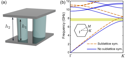
The valley hall lattices are implemented experimentally using ceramic pillars of refractive index , arranged in the space between parallel metal plates [Fig. 7(a)]. Since the experiment occurs in the microwave regime, the top and bottom plates act as perfect electrical conductors. The pillars are placed in a honeycomb-like lattice, have have radii and for the two sublattices. As the lattice is amorphous, there is a distribution of pillar separations; the lattice is scaled so the mean next nearest neighbor distance (roughly speaking, the lattice constant of the equivalent honeycomb lattice) is . All pillars have height .
For the static transmission measurements of Fig. 4, we set (i.e., the plates directly touch the pillars). Calculations on the equivalent 3D photonic crystal (i.e., an infinite perfectly crystalline lattice with the same structural parameters) show that the band structure is almost identical to that of a 2D lattice (like in the simulations of Fig. 3), with band gap at –.
For the field-mapping experiments (Figs. 2 and 5), we take (i.e., there is a air gap to avoid direct mechanical contact between the moving top plate and the pillars). The air gap induces a slight frequency shift relative to the 2D band structure. Fig. 7(b) plots the in-plane band structure of the equivalent crystal lattice with lattice constant . If the pillars on both sublattices have radius , there are two Dirac points at at the corners of the hexagonal Brillouin zone. If the pillars on the two sublattices have radii and , the band gap occurs at –.
Appendix C TDs in Photonic Graphene
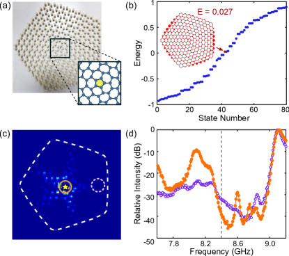
We fabricated an experimental sample based on an “photonic graphene” with a pentagonal TD in the center [Fig. 8(a)], i.e all pillars having equal radius . To help understand the qualitative implications of this lattice geometry, Fig. 8(b) plots the energy spectrum of a tight-binding model based on this lattice, with nearest neighbor hopping and on-site mass . As expected, there is no band gap. We examined the individual eigenstates and found none that are strongly localized at the TD; the intensity distribution of a typical eigenstate (with energy ) is shown in the inset to Fig. 8(b). This is consistent with previous theoretical analyses of topological defects in graphene Lammert and Crespi (2000, 2004); Rüegg and Lin (2013), which showed that such defects act upon Dirac cone states like a gauge field rather than a confining potential.
Fig. 8(c) plots the measured field intensity map with a dipole source (oriented perpendicular to the plane) placed at the TD. The source frequency is , close to the predicted Dirac frequency of [see Fig. 7(b)]. Unlike the VPCs shown in Fig. 2 in manuscript, no waveguiding is observed due to the lack of a disclination. The frequency dependence of the field intensity, plotted in Fig. 8(d), shows no apparent resonance associated with the topological defect.
Rüegg and Lin have found that if T is broken, topological defects in such lattices can generate localized bound states Rüegg and Lin (2013). Interestingly, such bound states are tied to the Chern number of the surrounding lattice and are robust against perturbations. In future work, photonic lattices could be used to to realize this theoretical prediction, either using magneto-optic materials to directly break T, or using three-dimensional structures in which an axial direction serves as an effective time Ozawa et al. (2019).
References
- Ozawa et al. (2019) T. Ozawa, H. M. Price, A. Amo, N. Goldman, M. Hafezi, L. Lu, M. C. Rechtsman, D. Schuster, J. Simon, O. Zilberberg, and I. Carusotto, Rev. Mod. Phys. 91, 015006 (2019).
- Bansil et al. (2016) A. Bansil, H. Lin, and T. Das, Rev. Mod. Phys. 88, 021004 (2016).
- Hafezi et al. (2011) M. Hafezi, E. A. Demler, M. D. Lukin, and J. M. Taylor, Nat. Phys. 7, 907 (2011).
- Wang et al. (2008) Z. Wang, Y. D. Chong, J. D. Joannopoulos, and M. Soljačić, Phys. Rev. Lett. 100, 013905 (2008).
- Wang et al. (2009) Z. Wang, Y. Chong, J. D. Joannopoulos, and M. Soljačić, Nature 461, 772 (2009).
- Dong et al. (2017) J.-W. Dong, X.-D. Chen, H. Zhu, Y. Wang, and X. Zhang, Nat. Mater. 16, 298 (2017).
- Shalaev et al. (2019) M. I. Shalaev, W. Walasik, A. Tsukernik, Y. Xu, and N. M. Litchinitser, Nat. Nanotech. 14, 31 (2019).
- Hadad et al. (2018) Y. Hadad, J. C. Soric, A. B. Khanikaev, and A. Alù, Nat. Electron. 1, 178 (2018).
- Wang et al. (2019) Y. Wang, L.-J. Lang, C. H. Lee, B. Zhang, and Y. D. Chong, Nat. Commun. 10, 1102 (2019).
- St-Jean et al. (2017) P. St-Jean, V. Goblot, E. Galopin, A. Lemaître, T. Ozawa, L. Le Gratiet, I. Sagnes, J. Bloch, and A. Amo, Nat. Photon 11, 651 (2017).
- Zhao et al. (2018) H. Zhao, P. Miao, M. H. Teimourpour, S. Malzard, R. El-Ganainy, H. Schomerus, and L. Feng, Nat. Commun. 9, 981 (2018).
- Parto et al. (2018) M. Parto, S. Wittek, H. Hodaei, G. Harari, M. A. Bandres, J. Ren, M. C. Rechtsman, M. Segev, D. N. Christodoulides, and M. Khajavikhan, Phys. Rev. Lett. 120, 113901 (2018).
- Ota et al. (2018) Y. Ota, R. Katsumi, K. Watanabe, S. Iwamoto, and Y. Arakawa, Commun. Phys. 1, 86 (2018).
- Bandres et al. (2018) M. A. Bandres, S. Wittek, G. Harari, M. Parto, J. Ren, M. Segev, D. N. Christodoulides, and M. Khajavikhan, Science 359, 4005 (2018).
- Harari et al. (2018) G. Harari, M. A. Bandres, Y. Lumer, M. C. Rechtsman, Y. D. Chong, M. Khajavikhan, D. N. Christodoulides, and M. Segev, Science 359, 4003 (2018).
- Ma and Shvets (2016) T. Ma and G. Shvets, New. J. Phys 18, 025012 (2016).
- Gao et al. (2017) F. Gao, H. Xue, Z. Yang, K. Lai, Y. Yu, X. Lin, Y. Chong, G. Shvets, and B. Zhang, Nat. Phys. 14, 140 (2017).
- He et al. (2019) X.-T. He, E.-T. Liang, J.-J. Yuan, H.-Y. Qiu, X.-D. Chen, F.-L. Zhao, and J.-W. Dong, Nat. Comm. 10, 872 (2019).
- Wu and Hu (2015) L.-H. Wu and X. Hu, Phys. Rev. Lett. 114, 223901 (2015).
- Barik et al. (2018) S. Barik, A. Karasahin, C. Flower, T. Cai, H. Miyake, W. DeGottardi, M. Hafezi, and E. Waks, Science 359, 666 (2018).
- Mermin (1979) N. D. Mermin, Rev. Mod. Phys. 51, 591 (1979).
- Kosterlitz (2017) J. M. Kosterlitz, Rev. Mod. Phys. 89, 040501 (2017).
- González et al. (1993) J. González, F. Guinea, and M. A. H. Vozmediano, Nucl. Phys. B 406, 771 (1993).
- Lammert and Crespi (2000) P. E. Lammert and V. H. Crespi, Phys. Rev. Lett. 85, 5190 (2000).
- Vozmediano et al. (2010) M. A. H. Vozmediano, M. I. Katsnelson, and F. Guinea, Phys. Rep. 496, 109 (2010).
- Kotakoski et al. (2011) J. Kotakoski, A. V. Krasheninnikov, U. Kaiser, and J. C. Meyer, Phys. Rev. Lett. 106, 105505 (2011).
- de Souza et al. (2014) J. de Souza, C. de Lima Ribeiro, and C. Furtado, Physics Letters A 378, 2317–2324 (2014).
- Yazyev and Louie (2010) O. V. Yazyev and S. G. Louie, Nat. Mater. 9, 806 (2010).
- Lahiri et al. (2010) J. Lahiri, Y. Lin, P. Bozkurt, I. I. Oleynik, and M. Batzill, Nat. Nanotech. 5, 326 (2010).
- Huang et al. (2011) P. Y. Huang, C. S. Ruiz-Vargas, A. M. van der Zande, W. S. Whitney, M. P. Levendorf, J. W. Kevek, S. Garg, J. S. Alden, C. J. Hustedt, Y. Zhu, J. Park, P. L. McEuen, and D. A. Muller, Nature 469, 389 (2011).
- Warner et al. (2012) J. H. Warner, E. R. Margine, M. Mukai, A. W. Robertson, F. Giustino, and A. I. Kirkland, Science 337, 209 (2012).
- Plotnik et al. (2014) Y. Plotnik, M. C. Rechtsman, D. Song, M. Heinrich, J. M. Zeuner, S. Nolte, Y. Lumer, N. Malkova, J. Xu, A. Szameit, and et al., Nature Materials 13, 57–62 (2014).
- Rüegg and Lin (2013) A. Rüegg and C. Lin, Phys. Rev. Lett. 110, 046401 (2013).
- Miyazaki et al. (2003) H. Miyazaki, M. Hase, H. T. Miyazaki, Y. Kurokawa, and N. Shinya, Phys. Rev. B 67, 235109 (2003).
- Edagawa et al. (2008) K. Edagawa, S. Kanoko, and M. Notomi, Phys. Rev. Lett. 100, 013901 (2008).
- Florescu et al. (2009) M. Florescu, S. Torquato, and P. J. Steinhardt, Proc. Natl. Acad. Sci. 106, 20658–20663 (2009).
- Yang et al. (2010) J.-K. Yang, C. Schreck, H. Noh, S.-F. Liew, M. I. Guy, C. S. O’Hern, and H. Cao, Phys. Rev. A 82, 053838 (2010).
- Imagawa et al. (2010) S. Imagawa, K. Edagawa, K. Morita, T. Niino, Y. Kagawa, and M. Notomi, Phys. Rev. B 82, 115116 (2010).
- Man et al. (2013) W. Man, M. Florescu, E. P. Williamson, Y. He, S. R. Hashemizad, B. Y. C. Leung, D. R. Liner, S. Torquato, P. M. Chaikin, and P. J. Steinhardt, Proc. Natl. Acad. Sci. 110, 15886–15891 (2013).
- Florescu et al. (2013) M. Florescu, P. J. Steinhardt, and S. Torquato, Phys. Rev. B 87, 165116 (2013).
- Kramer and MacKinnon (1993) B. Kramer and A. MacKinnon, Rep. Prog. Phys. 56, 1469–1564 (1993).
- Bandres et al. (2016) M. A. Bandres, M. C. Rechtsman, and M. Segev, Phys. Rev. X 6, 011016 (2016).
- Mitchell et al. (2018) N. P. Mitchell, L. M. Nash, D. Hexner, A. M. Turner, and W. T. M. Irvine, Nat. Phys. 14, 380–385 (2018).
- Lammert and Crespi (2004) P. E. Lammert and V. H. Crespi, Phys. Rev. B 69, 035406 (2004).
- Plimpton (1995) S. Plimpton, J. Comp. Phys. 117, 1 (1995).
- Mansha et al. (2016) S. Mansha, Y. Zeng, Q. J. Wang, and Y. D. Chong, Opt. Express 24, 4890 (2016).
- Cheng et al. (2016) X. Cheng, C. Jouvaud, X. Ni, S. H. Mousavi, A. Z. Genack, and A. B. Khanikaev, Nat. Mater. 15, 542–548 (2016).
- Noh et al. (2018) J. Noh, W. A. Benalcazar, S. Huang, M. J. Collins, K. P. Chen, T. L. Hughes, and M. C. Rechtsman, Nat. Photon 12, 408 (2018).
- Sitenko and Vlasii (2007) Y. A. Sitenko and N. D. Vlasii, Nucl. Phys. B 787, 241 (2007).
- Cortijo and Vozmediano (2007) A. Cortijo and M. A. Vozmediano, Eur. Phys. J. Spec. Top. 148, 83 (2007).
- Jeong et al. (2008) B. W. Jeong, J. Ihm, and G.-D. Lee, Phys. Rev. B 78, 165403 (2008).
- Wei et al. (2012) Y. Wei, J. Wu, H. Yin, X. Shi, R. Yang, and M. Dresselhaus, Nat. Mater 11, 759 (2012).