Towards bright and pure single photon emitters at 300 K based on GaN quantum dots on silicon
Abstract
Quantum dots (QDs) based on III-nitride semiconductors are promising for single photon emission at non-cryogenic temperatures due to their large exciton binding energies. Here, we demonstrate GaN QD single photon emitters operating at 300 K with under continuous wave excitation. At this temperature, single photon emission rates up to 6 106 s-1 are reached while is maintained. Our results are achieved for GaN QDs embedded in a planar AlN layer grown on silicon, representing a promising pathway for future interlinkage with optical waveguides and cavities. These samples allow exploring the limiting factors to key performance metrics for single photon sources, such as brightness and single photon purity. While high brightness is assured by large exciton binding energies, the single photon purity is mainly affected by the spectral overlap with the biexcitonic emission. Thus, the performance of a GaN QD as a single photon emitter depends on the balance between the emission linewidth and the biexciton binding energy. We identify small GaN QDs with an emission energy in excess of 4.2 eV as promising candidates for future room temperature applications, since the biexciton binding energy becomes comparable to the average emission linewidth of around 55 meV.
Quantum dots (QDs) based on III-V semiconductors have attracted a lot of attention for their use as non-classical light sources, with the single photon source being the simplest and most elemental representative. Such a source of single photons should be as bright as possible, while retaining a high single photon purity Senellart et al. (2017); Schweickert et al. (2018). However, key metrics for such QD-based single photon sources are usually achieved at cryogenic temperatures with the seminal In(Ga)As/(Al)GaAs system Dou et al. (2008); Dusanowski et al. (2015); Cavigli et al. (2012). Identifying a material platform that can enable sufficiently performant single photon sources up to room temperature remains a challenging quest. In this respect, the main contenders are point defects in wide-bandgap semiconductors (2D materials He et al. (2015) and bulk semiconductors Castelletto et al. (2014); Morfa et al. (2012)), nitrogen and silicon vacancies in diamond Aharonovich et al. (2011), as well as semiconductor QDs Michler et al. (2000); Tribu et al. (2008); Lin et al. (2017). It would be advantageous to employ a material system with high integrability into a suitable photonic environment that offers epitaxial control. In this regard, III-nitrides offer a unique possibility as bipolar doping can be achieved, foreign and homoepitaxial substrates are available, and growth and processing techniques are well established, leading to their widespread implementation at an industrial scale for solid state lighting.
III-nitrides have shown promising advances in terms of single photon emission (SPE) by employing GaN/AlN Santori et al. (2005); Kako et al. (2006), GaN/AlGaN Holmes et al. (2014); Arita et al. (2017) and InGaN/GaN QDs Kremling et al. (2012); Jemsson et al. (2015); Wang et al. (2017); Gačević et al. (2017); Cho et al. (2018). Furthermore, SPE at temperatures as high as 350 K Holmes et al. (2016) and two-photon emission up to 50 K Callsen et al. (2013) have been demonstrated. The progress towards room temperature operation is directly linked to the exciton-phonon coupling. With rising temperature the phonon bath becomes increasingly populated. Optical and acoustic phonon populations can lead to effects such as charge carrier escape from the trapping potential of the QD reducing the brightness Holmes et al. (2016); Dou et al. (2008); Dusanowski et al. (2015); Cavigli et al. (2012) and emission linewidth broadening Krummheuer et al. (2002); Rol et al. (2007); Holmes et al. (2013); Ostapenko et al. (2012). The latter, is directly linked to the process of dephasing Callsen et al. (2013), which also limits the coherent manipulation of excitonic qubits Holmes et al. (2013); Thoma et al. (2016). For these reasons, the exciton-phonon interaction is generally considered as detrimental for QD-based single photon sources. Interestingly, for the specific case of GaN/AlN QDs a benefit can be drawn from the particularly strong exciton-phonon coupling Callsen et al. (2015). Hönig et al. Hönig et al. (2014) have shown that the biexciton cascade in GaN/AlN QDs often requires a phonon-mediated spin flip process in order to decay into the QD ground state.
In this work we explore key performance metrics of GaN/AlN QDs directly grown on Si(111) substrate. This choice of substrate would allow for future integration of the QDs into photonic nanostructures, owing to the high etching selectivity between the two material systems Vico Triviño et al. (2013); Roland et al. (2014); Rousseau et al. (2017). Furthermore, the balance between detrimental and beneficial effects induced by the exciton-phonon coupling is assessed. Thus, GaN/AlN single QDs are shown to be bright single photon sources with count rates at the sample surface on the order of 106 - 107 s-1 at room temperature. Power-dependent second order autocorrelation function measurements () were carried out at room temperature and the traces examined in the framework of a multiple-level system including the biexciton (XX), higher order excitonic complexes, and spectral diffusion. All probed QDs displayed single photon characteristics at 300 K with an average = 0.23 and a minimum of = 0.17 0.08.
Results
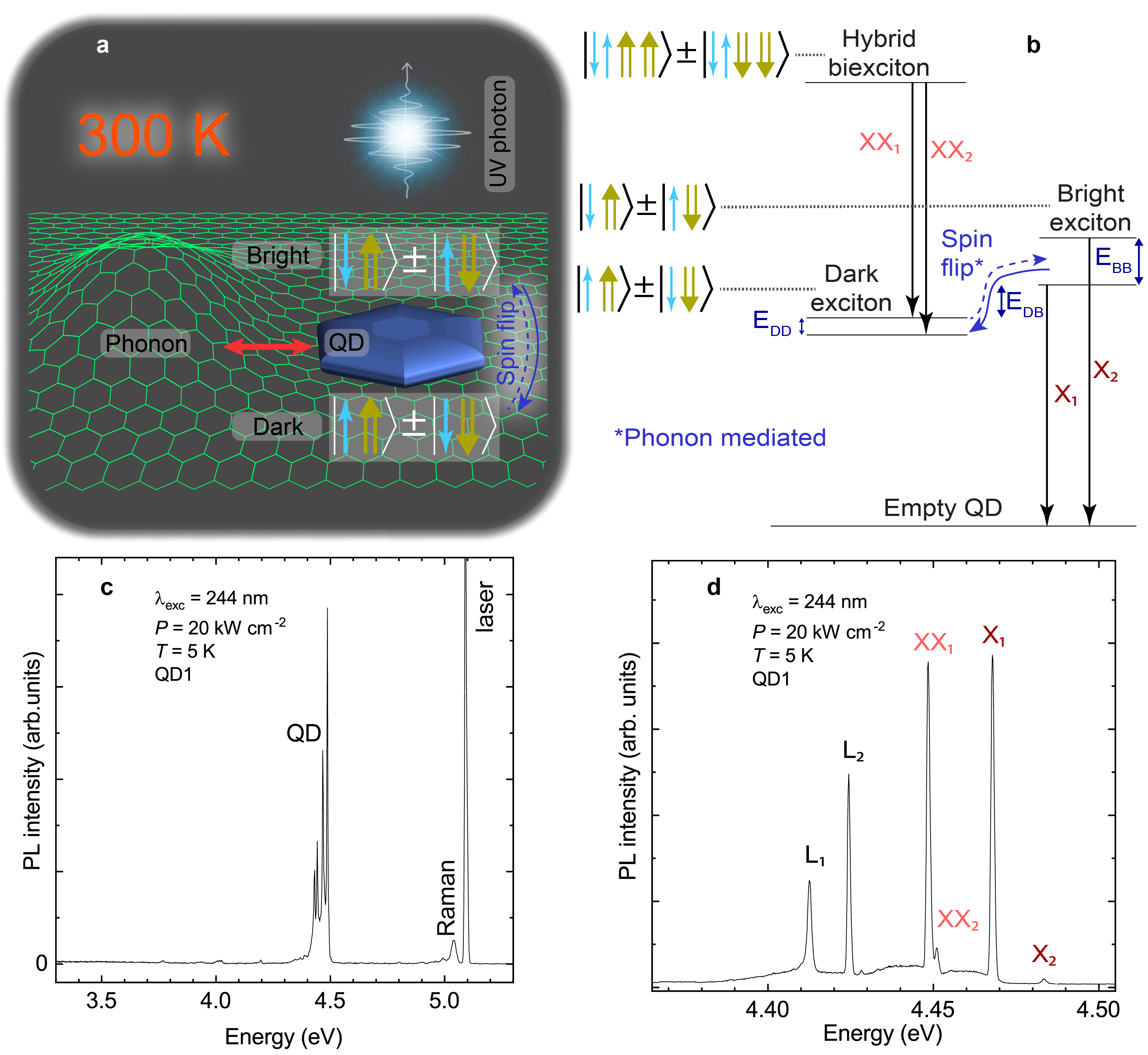
Phonons play an important role in the SPE process in GaN QDs as they provide the energy conservation for the spin flip from dark to bright excitons as illustrated in Fig. 1 a. Dark excitons are constantly generated in GaN QDs due to the presence of a so-called hybrid biexciton Hönig et al. (2014). In the hybrid biexciton, the two electrons have opposite spins, whereas the holes have parallel spins; which is the energetically stable configuration due to the occurrence of huge hole masses in GaN Rodina et al. (2001). For this spin configuration, the total spin of the electrons is = +1/2 -1/2 and that of the holes is = +(-) 3/2 +(-) 3/2 and hence the total excitonic angular momentum () of the hybrid biexciton amounts to = 3. A diagram of the relevant energy levels, their spin configurations and radiative transitions are displayed in Fig. 1 b. The hybrid biexciton-exciton cascade shown in Fig. 1 b deviates from the classical biexciton cascade; upon decay of the hybrid biexciton in a one-photon process ( = 1), conservation of angular momentum implies the population of the dark-exciton states with = 2. The dark excitons can then transition into bright exciton state with = 1 via a phonon-assisted spin flip process Labeau et al. (2003); Roszak et al. (2007); Hönig et al. (2014). This process is illustrated in Fig. 1 a and 1 b by the blue dashed arrow. The intricate physical mechanism behind the phonon-assisted spin flip process is still debated in literature Woods et al. (2002); Johansen et al. (2010); Khosla et al. (2018). This latter process depends on the thermal population of phonons and the dark to bright energy splitting (), see Fig. 1 b. The spin flip from bright to dark (solid blue arrow) requires the emission of a phonon and hence does not depend on temperature. As a consequence, the bright exciton states are thermally activated by the phonon-mediated spin flip. Further on, due to QD asymmetry, the bright states display fine structure splitting (FSS) Kindel et al. (2010) denoted by in Fig. 1 b. A similar, but smaller splitting occurs for the excitonic dark states, which is denoted by in Fig. 1 b Hönig et al. (2014).
A recurring feature of the optical signature of single GaN QDs at low temperature is the presence of several peaks, of which four peaks dominate in intensity (see further examples in the supplementary material). A broad energy range, low temperature micro-photoluminescence (-PL) spectrum of a typical GaN QD (QD1) is displayed in Fig. 1 c showcasing the absence of background emission, along with a high-resolution spectrum in Fig. 1 d. Some of these transitions were identified within the framework of the hybrid biexciton. The radiative decays of the hybrid biexciton into the exciton’s dark states (XX1 and XX2) and the exciton’s bright states (X1 and X2) are labeled in the -PL spectrum shown in Fig. 1 d in agreement with the solid, black arrows of Fig. 1 b. The identification of the lines was confirmed by power- and polarization-dependent measurements (see supplementary material). All lines are linearly polarized, with L1, L2, XX1 and X2 being cross polarized to XX2 and X1. The nature of the two lower energy peaks ( and ) is currently being investigated. The strong exciton-phonon interaction is already evident in the -PL spectrum of Fig. 1 d, as each peak is accompanied by a broad low energy side-band that is associated to acoustic phonons Ostapenko et al. (2012). Indeed, the emission characteristics and the radiative decay of the hybrid XX are heavily impacted by the exciton-phonon interaction as illustrated in Fig. 1 a.
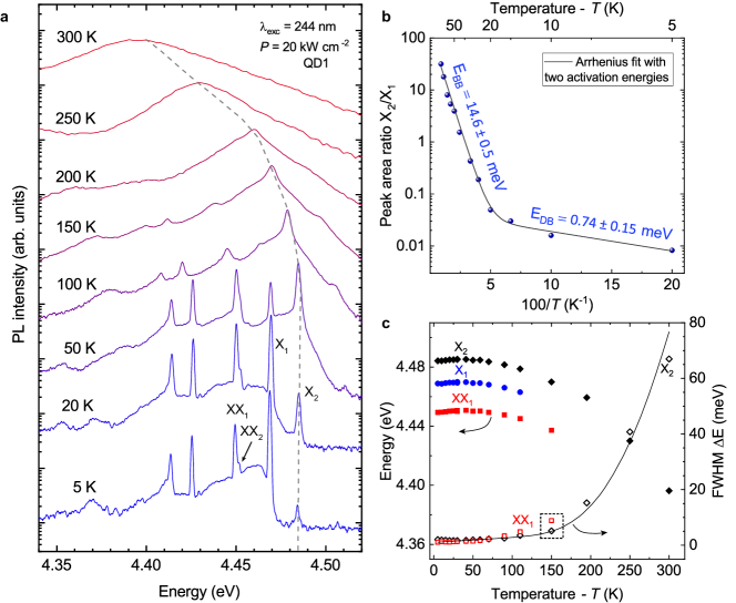
Since the spin flip from the dark to bright state is phonon mediated Hönig et al. (2014); Sallen et al. (2009); Fernée et al. (2009), temperature has an important role in the intensity of each transition. The -PL spectrum of QD1 is plotted in Fig. 2 a as a function of sample temperature. The excitation power density was set to 20 kW cm-2. As the temperature is increased, X2 rises in intensity and matches X1 at about 40 K. At a temperature of around 150 K the spectrum is completely dominated by X2. The intensity ratio of X1 and X2 was evaluated with the peak area and plotted as a function of temperature in Fig. 2 b. The data can be fitted with an Arrhenius equation and two activation energies, these energies approximate the dark to bright energy difference () and the bright () FSS Hönig et al. (2014) introduced in Fig. 1.
The energy and full width at half maximum (FWHM) of the bright states and the biexciton were followed throughout the investigated temperature range and are plotted in Fig. 2 c. The emission of X2 could be tracked over the whole temperature range. It redshifts by about 90 meV from 5 K to 300 K, which corresponds to that of the AlN matrix material Guo et al. (2001). Notice an additional blueshift in the temperature range from 5 to 40 K on the order of 1 meV, which could originate from the negative thermal expansion coefficient of AlN at low temperatures Figge et al. (2009). Simultaneously, the spectral line broadens to about 60 meV. The FWHM () was modeled (solid line in Fig. 2 c) using the following equation Fischer et al. (1997):
| (1) |
where is the inhomogeneous linewidth at 0 K, is the coupling to acoustic phonons, is the coupling to longitudinal optical phonons (LO) and is the energy of LO phonons. is readily available from the PL data and amounts to 102 meV. Callsen et al. found that the of GaN QDs scales from the value of unstrained GaN for large QDs towards that of AlN for small QDs. This is due to the exciton-LO-phonon interaction averaging over both the GaN QD and the AlN matrix surroundings Callsen et al. (2015). Then, the constants , , and were fitted to the data with resulting values of 1 0.1 meV, 18 2 eV/K, and 3.57 0.26 eV, respectively. The extracted value is larger than the one obtained by Demangeot et al. Demangeot et al. (2009), suggesting that the coupling strength to phonons is specific to each QD as illustrated by linewidth statistics. In Fig. 3 a, FWHM statistic at a sample temperature of 300 K is presented. The scatter yields an average value of 55 meV with a standard deviation of 7 meV (based on 112 emission lines). Fluctuating charges surrounding GaN QDs can lead to large inhomogeneous broadenings at low temperatures Kindel et al. (2014). The impact of fluctuating charges on the FWHM of single GaN QDs is exacerbated due to the quantum confined Stark effect present in polar III-nitride nanostructures. Hence, the linewidth measured at low temperature depends strongly on the excitonic dipole moment and therefore on the QD emission energy. As opposed to the low temperature case Kindel et al. (2014), no clear correlation could be observed between the emission energy and the linewidth, signaling a phonon dominated broadening. For a QD to provide SPE at 300 K, a biexciton binding energy () comparable to or larger than the linewidth is required in order to avoid spectral overlap. In Fig. 3 a, values found in the literature are plotted along with the two QDs presented in this work Holmes et al. (2019); Hönig et al. (2014); Simeonov et al. (2008). A trend of increasing as a function of emission energy can be deduced. At emission energies above 4.2 eV, can become comparable to the linewidth rendering small QDs emitting at higher energies even more appealing.
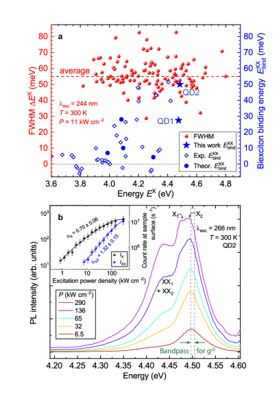
Excitation-power-dependent -PL measurements of QD2 are displayed in Fig. 3 b at a sample temperature of 300 K along with the bandpass employed for measurements. As the power is increased, an additional peak appears on the low energy side, which we suggest to identify as the XX. The integrated intensity of the peaks ( and for the exciton and biexciton, respectively) is marked in the inset of Fig. 3 b. The scaling of and with excitation power density was modeled with a Poisson distribution Grundmann and Bimberg (1997), where is the excitation power density and is the number of excitons present in the QD. A fit to the data yielded = 0.70 0.06 and = 1.32 0.15. The value of the exponents () are consistent with previous reports on hybrid biexcitons in GaN QDs Hönig et al. (2014).
A key feature of a practical single photon source is its brightness, which can be compared to other systems by considering the count rate at the sample surface Aharonovich et al. (2016). The brightness of the QD was estimated for the selected spectral band pass of 8 meV used during the -measurements. The brightness of QD2 was quantified by measuring the detection losses in the optical setup. At a temperature of 300 K and an excitation power of 6.5 kW cm-2, the count rate at the sample surface was estimated to be 1.9 ( 0.7) 106 s-1.
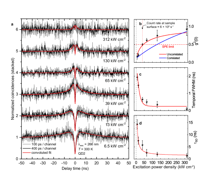
The -PL emission of these QDs, which is close to background free (see Fig. 1 c), together with the large values and count rates at the sample surface in the 106 s-1 regime, make these QDs suitable for SPE at 300 K. The performance of QD2 as a single photon source was probed as a function of excitation power density. The results are displayed in Fig. 4 a. The experimental traces were fitted with a multiple-level model for the biexciton-exciton cascade Kindel (2010) that also considers bunching due to spectral diffusion () Sallen et al. (2010) convoluted with the instrument response function (IRF):
| (2) |
where
| (3) |
is the second order autocorrelation function of the exciton, with , with the decay time and the pump rate. For vanishing excitation powers, tends to the two-level expression: Fox (2006). Time-resolved PL experiments performed on the QD ensemble at the same emission energy give access to , while and the spectral diffusion parameters are ascertained by a fit to the data shown in Fig. 4 a.
A clear room temperature antibunching can be observed at zero time delay proving SPE. At the lowest reported excitation power density, the single photon purity reaches = 0.17 0.08. However, as the excitation power density is increased, also increases and surpasses the single photon limit ( = 0.5) for an excitation power density of 39 kW cm-2 (see Fig. 4 b). At this excitation power density, the count rate at the sample surface amounts to 6 106 s-1.
The single photon purity seems to be mainly curtailed by the XX emission, cf. Fig. 3 b. A quantification of the spectral overlap of the X and XX emission is given in the supplementary material. Although a of 47 meV was measured for this specific QD, the XX broadening of this particular QD amounts to almost 80 meV and thus photons from the XX are also present in the investigated spectral window of 8 meV as depicted in Fig. 3b. Hence, for rising excitation powers an increasingly prominent luminescence background occurs in the X detection window due to the presence of XX. Thus, the photon stream is contaminated, which limits the achievable value. However, for a precise quantification of this limitation it is of utmost importance to determine whether the background luminescence is (a) correlated or (b) uncorrelated to the X emission.
Generally, in the biexciton-exciton cascade, the decay of XX and X should be temporally correlated, leading to a correlation between the two photon streams linked to XX and X. For the correlated case (a), the resulting values can be modeled as described in the supplementary material based on a multiexcitonic model, neglecting the dark excitons. Practically, as soon as the XX and X emissions overlap in the detection bandpass, all auto- and cross-correlation contributions to must be summed. As a result of the corresponding theoretical treatment, we obtain the blue, solid line in Fig. 4 b.
For case (b), the single photon purity can be estimated based on Sallen et al. Sallen et al. (2009):
| (4) |
The red, solid line in Fig. 4 b depicts a fit to the experimental values (considering the limited time resolution of the setup) based on equation 4. Here we consider and , as determined by the series of excitation-power-dependent spectra shown in Fig. 3 b and its inset. A surprisingly good agreement is found between the data and the theoretical treatment assuming an uncorrelated background emission, cf. Fig. 4 b. Interestingly, in contrast to case (a), the assumption of uncorrelated photon streams related to XX and X does not lead to an underestimation of as a function of excitation power density.
The observation that the assumption of an uncorrelated photon stream (case (b)) leads to a better agreement with the experiemental data than the assumption of a correlated photon stream (case (a)), could be understood in terms of the hybrid biexciton cascade depicted in Fig. 1 b. The spin-flip process between the dark and bright exciton states should randomize the emission of photons stemming from the overall cascade. However, based on the present measurements, the balance between the correlated and uncorrelated contributions to the overall background emission, which degrade the values, remains obscured. Therefore, future measurements should target auto- and cross-correlation analyses for X and XX with variable bandpasses. Clearly, also a better trade-off between and the occurring FWHM can be found as suggested by the data shown in Fig. 3 a.
The loss in single photon purity with increasing excitation power density is accompanied by a narrowing of the antibunching peak as shown in Fig. 4 a. In Fig. 4 c, we plot the corresponding FWHM of the antibunching peak as a function of excitation power density. For the considered multiple-level system, this temporal FWHM can be calculated by inverting equation 3:
| (5) |
where is the Lambert function. Although a narrowing of the antibunching peak is not inherently detrimental to the SPE performance, it can impact the uncertainty of the measurements as the setup’s temporal resolution is approached.
Another salient feature of the -measurements is the appearance of a photon bunching phenomenon overlapping with the antibunching signature. Following the analysis of Sallen et al. Sallen et al. (2010), we assume that this bunching is due to spectral diffusion as the emission shifts in and out of the detection window, cf. Fig. 3 b. With increasing excitation power density the characteristic time of the bunching () decreases. This is due to the fact that the rate of spectral diffusion mostly depends on the occupation probability of charge trapping defects near the QD, which in turn depends on the excitation power density: Holmes et al. (2015); Gao et al. (2019).
Finally, measurements were performed on several QDs at 300 K with an excitation power density of 20 kW cm-2. QDs with an emission energy between 4.4 and 4.6 eV and large values were selected in order to maintain the validity of the previous discussion. All measured QDs displayed antibunching (see supplementary material). The average value amounted to 0.23 0.05. The high yield of GaN QDs displaying SPE at 300 K together with the high count rates and the use of Si substrates pave a promising pathway towards future integration of these QDs into integrated photonic platforms. For example, integration of a QD into an optical cavity has been shown to increase the indistinguishability of the photons as it decreases phonon decoherence processes which are particularly pronounced at elevated temperatures Grange et al. (2017). Further on, quantum frequency down-conversion schemes such as the one presented by Zaske et al. Zaske et al. (2012), enable the conversion of QD based single photon sources to telecom wavelengths.
Summary
In conclusion we have demonstrated that self-assembled GaN/AlN QDs on Si substrates can provide SPE at 300 K. Their spectral signature and their behavior with temperature can be explained by a hybrid XX model and strong exciton-phonon interaction. These QDs remain bright even at room temperature, with typical count rates at the sample surface on the order of 106 - 107 s-1. Photon statistics displayed an enhanced single photon purity for low excitation powers due to the suppressed contribution of the XX. The overlapping bunching in the is explained in terms of spectral diffusion. The probed QDs exhibited SPE at 300 K with an average value and a minimum value of .
Methods
The sample was grown by NH3-molecular beam epitaxy (MBE). It consists of 100 nm of high temperature AlN on Si(111), followed by a plane of GaN QDs, a 20 nm AlN top barrier and finally a second plane of GaN QDs. Further details on the growth of the AlN layer and the QDs can be found in Refs. Tamariz et al. (2017, 2019). The top QD plane was used for atomic force microscopy (AFM) and subsequently evaporated in the MBE reactor under vacuum at a temperature of 800 ∘C. Mesa structures and position markers were then fabricated by e-beam lithography. The developed regions of the resist were etched down to a depth of about 60 nm, so that no QDs remain outside of the mesa and marker structures. The mesa sizes range from 2 m to 50 nm in diameter. From AFM measurements, the QD density was estimated to be 1010 cm-2 (see supplementary material). Furthermore, AFM revealed a broad QD size distribution, which is advantageous for the study of the optical features of QDs emitting over a wide range of energies.
The optical properties were investigated by -PL spectroscopy. The QDs were excited either with a 266 nm or a 244 nm continuous wave laser. The sample has a very thin wetting layer, estimated at a thickness of 1.5 ML, that is not excited with the employed lasers. The sample was loaded in a closed-cycle He cryostat (Cryostation C2 from Montana Instruments, Inc.) and the luminescence was collected by an 80 infinity corrected microscope objective suited for the ultraviolet spectral range (NA = 0.55). The laser spot size was estimated to have a diameter of 1 m. The luminescence is then routed either to a high resolution spectrometer or a Hanbury Brown and Twiss interferometer for measurements.
Supplementary material
See supplementary material for additional structural and spectroscopic information, as well as the treatment of correlated emission in the measurements.
Acknowledgements
This work was supported by the Swiss National Science Foundation through Grant 200021E_15468 and 200020_162657 and by the Marie Sklodowska-Curie action “PhotoHeatEffect" (Grant No. 749565) within the European Union’s Horizon 2020 research and innovation program.
Author contribution
S.T., G.C. and J.S. performed the optical measurements. S.T. grew the sample and K.S. performed the nano-mesa fabrication. S.T., G.C., J.S. and R.B. analyzed the data. S.T. and G.C. wrote the manuscript with contributions from all authors. N.G. initiated and supervised the entire project.
References
- Senellart et al. (2017) P. Senellart, G. Solomon, and A. White, Nat. Nanotechnol. 12, 1026 (2017).
- Schweickert et al. (2018) L. Schweickert, K. D. Jöns, K. D. Zeuner, S. F. Covre da Silva, H. Huang, T. Lettner, M. Reindl, J. Zichi, R. Trotta, A. Rastelli, and V. Zwiller, Appl. Phys. Lett. 112, 093106 (2018).
- Dou et al. (2008) X. M. Dou, X. Y. Chang, B. Q. Sun, Y. H. Xiong, Z. C. Niu, S. S. Huang, H. Q. Ni, Y. Du, and J. B. Xia, Appl. Phys. Lett. 93, 101107 (2008).
- Dusanowski et al. (2015) Ł. Dusanowski, M. Syperek, A. Maryński, L. H. Li, J. Misiewicz, S. Höfling, M. Kamp, A. Fiore, and G. Sȩk, Appl. Phys. Lett. 106, 233107 (2015).
- Cavigli et al. (2012) L. Cavigli, S. Bietti, N. Accanto, S. Minari, M. Abbarchi, G. Isella, C. Frigeri, A. Vinattieri, M. Gurioli, and S. Sanguinetti, Appl. Phys. Lett. 100, 231112 (2012).
- He et al. (2015) Y. M. He, G. Clark, J. R. Schaibley, Y. He, M. C. Chen, Y. J. Wei, X. Ding, Q. Zhang, W. Yao, X. Xu, C. Y. Lu, and J. W. Pan, Nat. Nanotechnol. 10, 497 (2015).
- Castelletto et al. (2014) S. Castelletto, B. C. Johnson, V. Ivády, N. Stavrias, T. Umeda, A. Gali, and T. Ohshima, Nat. Mater. 13, 151 (2014).
- Morfa et al. (2012) A. J. Morfa, B. C. Gibson, M. Karg, T. J. Karle, A. D. Greentree, P. Mulvaney, and S. Tomljenovic-Hanic, Nano Lett. 12, 949 (2012).
- Aharonovich et al. (2011) I. Aharonovich, A. D. Greentree, and S. Prawer, Nat. Photonics 5, 397 (2011).
- Michler et al. (2000) P. Michler, A. Imamoğlu, M. D. Mason, P. J. Carson, G. F. Strouse, and S. K. Buratto, Nature 406, 968 (2000).
- Tribu et al. (2008) A. Tribu, G. Sallen, T. Aichele, R. André, J.-P. Poizat, C. Bougerol, S. Tatarenko, and K. Kheng, Nano Lett. 8, 4326 (2008).
- Lin et al. (2017) X. Lin, X. Dai, C. Pu, Y. Deng, Y. Niu, L. Tong, W. Fang, Y. Jin, and X. Peng, Nat. Commun. 8, 1132 (2017).
- Santori et al. (2005) C. Santori, S. Götzinger, Y. Yamamoto, S. Kako, K. Hoshino, and Y. Arakawa, Appl. Phys. Lett. 87, 051916 (2005), 0502013 [cond-mat] .
- Kako et al. (2006) S. Kako, C. Santori, K. Hoshino, S. Götzinger, Y. Yamamoto, and Y. Arakawa, Nat. Mater. 5, 887 (2006).
- Holmes et al. (2014) M. J. Holmes, K. Choi, S. Kako, M. Arita, and Y. Arakawa, Nano Lett. 14, 982 (2014).
- Arita et al. (2017) M. Arita, F. Le Roux, M. J. Holmes, S. Kako, and Y. Arakawa, Nano Letters 17, 2902 (2017).
- Kremling et al. (2012) S. Kremling, C. Tessarek, H. Dartsch, S. Figge, S. Höfling, L. Worschech, C. Kruse, D. Hommel, and A. Forchel, Appl. Phys. Lett. 100, 061115 (2012).
- Jemsson et al. (2015) T. Jemsson, H. Machhadani, P. O. Holtz, and K. F. Karlsson, Nanotechnology 26, 065702 (2015).
- Wang et al. (2017) T. Wang, T. J. Puchtler, T. Zhu, J. C. Jarman, L. P. Nuttall, R. A. Oliver, and R. A. Taylor, Nanoscale 9, 9421 (2017).
- Gačević et al. (2017) Ž. Gačević, M. Holmes, E. Chernysheva, M. Müller, A. Torres-Pardo, P. Veit, F. Bertram, J. Christen, J. M. González Calbet, Y. Arakawa, E. Calleja, and S. Lazić, ACS Photonics 4, 657 (2017).
- Cho et al. (2018) J. H. Cho, Y. M. Kim, S. H. Lim, H. S. Yeo, S. Kim, S. H. Gong, and Y. H. Cho, ACS Photonics 5, 439 (2018).
- Holmes et al. (2016) M. J. Holmes, S. Kako, K. Choi, M. Arita, and Y. Arakawa, ACS Photonics 3, 543 (2016).
- Callsen et al. (2013) G. Callsen, A. Carmele, G. Hönig, C. Kindel, J. Brunnmeier, M. R. Wagner, E. Stock, J. S. Reparaz, A. Schliwa, S. Reitzenstein, A. Knorr, A. Hoffmann, S. Kako, and Y. Arakawa, Phys. Rev. B 87, 245314 (2013).
- Krummheuer et al. (2002) B. Krummheuer, V. M. Axt, and T. Kuhn, Phys. Rev. B 65, 195313 (2002).
- Rol et al. (2007) F. Rol, S. Founta, H. Mariette, B. Daudin, L. S. Dang, J. Bleuse, D. Peyrade, J.-M. Gérard, and B. Gayral, Phys. Rev. B 75, 125306 (2007).
- Holmes et al. (2013) M. Holmes, S. Kako, K. Choi, P. Podemski, M. Arita, and Y. Arakawa, Phys. Rev. Lett. 111, 057401 (2013).
- Ostapenko et al. (2012) I. A. Ostapenko, G. Hönig, S. Rodt, A. Schliwa, A. Hoffmann, D. Bimberg, M. R. Dachner, M. Richter, A. Knorr, S. Kako, and Y. Arakawa, Phys. Rev. B 85, 081303(R) (2012).
- Thoma et al. (2016) A. Thoma, P. Schnauber, M. Gschrey, M. Seifried, J. Wolters, J. H. Schulze, A. Strittmatter, S. Rodt, A. Carmele, A. Knorr, T. Heindel, and S. Reitzenstein, Phys. Rev. Lett. 116, 033601 (2016).
- Callsen et al. (2015) G. Callsen, G. M. O. Pahn, S. Kalinowski, C. Kindel, J. Settke, J. Brunnmeier, C. Nenstiel, T. Kure, F. Nippert, A. Schliwa, A. Hoffmann, T. Markurt, T. Schulz, M. Albrecht, S. Kako, M. Arita, and Y. Arakawa, Phys. Rev. B 92, 235439 (2015).
- Hönig et al. (2014) G. Hönig, G. Callsen, A. Schliwa, S. Kalinowski, C. Kindel, S. Kako, Y. Arakawa, D. Bimberg, and A. Hoffmann, Nat. Commun. 5, 5721 (2014).
- Vico Triviño et al. (2013) N. Vico Triviño, U. Dharanipathy, J.-F. Carlin, Z. Diao, R. Houdré, and N. Grandjean, Appl. Phys. Lett. 102, 081120 (2013).
- Roland et al. (2014) I. Roland, Y. Zeng, Z. Han, X. Checoury, C. Blin, M. El Kurdi, A. Ghrib, S. Sauvage, B. Gayral, C. Brimont, T. Guillet, F. Semond, and P. Boucaud, Appl. Phys. Lett. 105, 011104 (2014).
- Rousseau et al. (2017) I. Rousseau, I. Sánchez-Arribas, K. Shojiki, J.-F. Carlin, R. Butté, and N. Grandjean, Phys. Rev. B 95, 125313 (2017).
- Rodina et al. (2001) A. V. Rodina, M. Dietrich, A. Göldner, L. Eckey, A. Hoffmann, A. L. Efros, M. Rosen, and B. K. Meyer, Phys. Rev. B 64, 115204 (2001).
- Labeau et al. (2003) O. Labeau, P. Tamarat, and B. Lounis, Phys. Rev. Lett. 90, 257404 (2003).
- Roszak et al. (2007) K. Roszak, V. M. Axt, T. Kuhn, and P. Machnikowski, Phys. Rev. B 76, 195324 (2007).
- Woods et al. (2002) L. M. Woods, T. L. Reinecke, and Y. Lyanda-Geller, Phys. Rev. B 66, 161318(R) (2002).
- Johansen et al. (2010) J. Johansen, B. Julsgaard, S. Stobbe, J. M. Hvam, and P. Lodahl, Phys. Rev. B 81, 081304 (2010).
- Khosla et al. (2018) M. Khosla, S. Rao, and S. Gupta, Sci. Rep. 8, 8385 (2018).
- Kindel et al. (2010) C. Kindel, S. Kako, T. Kawano, H. Oishi, Y. Arakawa, G. Hönig, M. Winkelnkemper, A. Schliwa, A. Hoffmann, and D. Bimberg, Phys. Rev. B 81, 241309(R) (2010).
- Sallen et al. (2009) G. Sallen, A. Tribu, T. Aichele, R. André, L. Besombes, C. Bougerol, S. Tatarenko, K. Kheng, and J. P. Poizat, Phys. Rev. B 80, 085310 (2009).
- Fernée et al. (2009) M. J. Fernée, B. N. Littleton, and H. Rubinsztein-Dunlop, ACS Nano 3, 3762 (2009).
- Guo et al. (2001) Q. Guo, M. Nishio, H. Ogawa, and A. Yoshida, Phys. Rev. B 64, 113105 (2001).
- Figge et al. (2009) S. Figge, H. Kröncke, D. Hommel, and B. M. Epelbaum, Applied Physics Letters 94, 101915 (2009).
- Fischer et al. (1997) A. J. Fischer, W. Shan, G. H. Park, J. J. Song, D. S. Kim, D. S. Yee, R. Horning, and B. Goldenberg, Phys. Rev. B 56, 1077 (1997).
- Demangeot et al. (2009) F. Demangeot, D. Simeonov, A. Dussaigne, R. Butté, and N. Grandjean, Phys. Status Solidi C 6, S598 (2009).
- Kindel et al. (2014) C. Kindel, G. Callsen, S. Kako, T. Kawano, H. Oishi, G. Hönig, A. Schliwa, A. Hoffmann, and Y. Arakawa, Phys. Status Solidi Rapid Res. Lett. 8, 408 (2014).
- Holmes et al. (2019) M. J. Holmes, M. Arita, and Y. Arakawa, Semicond. Sci. Technol. 34, 033001 (2019).
- Simeonov et al. (2008) D. Simeonov, A. Dussaigne, R. Butté, and N. Grandjean, Phys. Rev. B 77, 075306 (2008).
- Grundmann and Bimberg (1997) M. Grundmann and D. Bimberg, Phys. Rev. B 55, 9740 (1997).
- Aharonovich et al. (2016) I. Aharonovich, D. Englund, and M. Toth, Nat. Photonics 10, 631 (2016).
- Kindel (2010) C. H. Kindel, Study on Optical Polarization in Hexagonal Gallium Nitride Quantum Dots, Ph.D. thesis, The University of Tokyo (2010).
- Sallen et al. (2010) G. Sallen, A. Tribu, T. Aichele, R. André, L. Besombes, C. Bougerol, M. Richard, S. Tatarenko, K. Kheng, and J.-P. Poizat, Nat. Photonics 4, 696 (2010).
- Fox (2006) M. Fox, Quantum optics: an introduction, Vol. 15 (Oxford University Press, 2006).
- Holmes et al. (2015) M. Holmes, S. Kako, K. Choi, M. Arita, and Y. Arakawa, Phys. Rev. B 92, 115447 (2015).
- Gao et al. (2019) K. Gao, H. Springbett, T. Zhu, R. A. Oliver, Y. Arakawa, and M. J. Holmes, Appl. Phys. Lett. 114, 112109 (2019).
- Grange et al. (2017) T. Grange, N. Somaschi, C. Antón, L. De Santis, G. Coppola, V. Giesz, A. Lemaître, I. Sagnes, A. Auffèves, and P. Senellart, Phys. Rev. Lett. 118, 253602 (2017).
- Zaske et al. (2012) S. Zaske, A. Lenhard, C. A. Keßler, J. Kettler, C. Hepp, C. Arend, R. Albrecht, W. M. Schulz, M. Jetter, P. Michler, and C. Becher, Phys. Rev. Lett. 109, 147404 (2012), 1204.6253 .
- Tamariz et al. (2017) S. Tamariz, D. Martin, and N. Grandjean, J. Cryst. Growth 476, 58 (2017).
- Tamariz et al. (2019) S. Tamariz, G. Callsen, and N. Grandjean, Appl. Phys. Lett. 114, 082101 (2019).