Optimal architecture for diamond-based wide-field thermal imaging
Abstract
Nitrogen-Vacancy centers in diamond possess an electronic spin resonance that strongly depends on temperature, which makes them efficient temperature sensor with a sensitivity down to a few mK/. However, the high thermal conductivity of the host diamond may strongly damp any temperature variations, leading to invasive measurements when probing local temperature distributions. In view of determining possible and optimal configurations for diamond-based wide-field thermal imaging, we here investigate, both experimentally and numerically, the effect of the presence of diamond on microscale temperature distributions. Three geometrical configurations are studied: a bulk diamond substrate, a thin diamond layer bonded on quartz and diamond nanoparticles dispersed on quartz. We show that the use of bulk diamond substrates for thermal imaging is highly invasive, in the sense that it prevents any substantial temperature increase. Conversely, thin diamond layers partly solve this issue and could provide a possible alternative for microscale thermal imaging. Dispersions of diamond nanoparticles throughout the sample appear as the most relevant approach as they do not affect the temperature distribution, although NV centers in nanodiamonds yield lower temperature sensitivities compared to bulk diamond.
Thermal imaging, enabling fast and accurate monitoring of heat distribution at sub-micron scales, has become decisive in a broad range of fields from exploratory research up to prototyping and manufacturing in nanomaterials science, nanoelectronics, nanophotonics or nanochemistry. Various detection schemes are being explored in this respect Quintanilla and Liz-Marzand (2018). These schemes include tip-enhanced infrared or Raman thermometry Weng et al. (2018); Li et al. (2018), scanning thermal microscopy (SThM) Majundar (1999); Gomes, Assy, and Chapuis (2015), SQUID-based nano-thermometry Halbertal et al. (2016) or nanoscale fluorescence thermometry making use of fluorescent nanoparticles either dispersed on the probed sample or attached to the tip of an atomic force microscope (AFM) Aigouy et al. (2005). Yet none of these techniques can simultaneously provide fast, sensitive (in the sub-K/ range), and quantitative thermal imaging with a sub-micron spatial resolution under ambient conditions.
Nitrogen-Vacancy (NV) centers in diamond have garnered growing attention in the last decade, notably because their electron spin resonance can be detected optically Gruber et al. (1997) and strongly depends on various external perturbations. This dependence has enabled to implement highly sensitive NV-based quantum sensors capable to locally probe several physical quantities including strain Trusheim and Englund (2016); Broadway et al. (2019), electric Dolde et al. (2011); Michl et al. (2019) and magnetic fields Degen, Reinhard, and Cappellaro (2017); Rondin et al. (2014); Levine et al. (2019). The sensing capabilities of the NV center have also been extended to thermometry Kucsko et al. (2013), building on the variation of the zero-field splitting parameter of its electron spin sublevels with temperature Acosta et al. (2010). A thermal sensitivity in the range of mK/ was demonstrated for single NV centers hosted in nanodiamonds Neumann et al. (2013) and can reach values down to few mK/ while using NV centers with long spin coherence times embedded in ultrapure bulk diamond samples Kucsko et al. (2013); Wang et al. (2015); Neumann et al. (2013); Toyli et al. (2013). Besides building on the temperature dependance of the spin resonance, temperature sensing with NV centers in diamond, can utilize the temperature dependance of their optical response (Debye-Waller factor, zero-phonon line or Anti-Stokes photoluminescence wavelength)Tran et al. (2019); Plakhotnik et al. (2014); such all-optical schemes have also been extended to other point defects in diamond, including SiV, GeV or SnV colored centers Nguyen et al. (2018); Fan et al. (2018); Alkahtani et al. (2018). Last but not least, the temperature sensitivities of NV centers can be pushed down to few tens K/, by relying on a transduction of temperature gradients on magnetic fields probed by their electronic spinsWang et al. (2018); Liu et al. (2019).
These thermal sensing modalities can be exploited for thermal imaging. A first strategy consists in grafting a NV-doped nanodiamond at the apex of either an optical fiber or an AFM tip, which is scanned above the surface of the sample to be probed Fedotov et al. (2014); Laraoui et al. (2015); Tetienne et al. (2016). The spatial resolution of thermal imaging is then ultimately limited by the nanodiamond size. Such a scanning-NV configuration however requires a complex experimental apparatus and suffers from long acquisition times. In addition, the thermal sensitivity is impaired by the short spin coherence time of NV centers hosted in nanodiamonds. Another approach makes use of stationary NV centers in a wide-field detection scheme Neumann et al. (2013); Wang et al. (2015); Andrich et al. (2018). Although the spatial resolution is then fundamentally limited by diffraction ( nm), this approach offers faster acquisition times and a simple experimental configuration. To date, wide-field thermal imaging has been solely demonstrated with NV-doped nanodiamonds directly dispersed on the surface of a target sample.
In this paper, we investigate whether this method could be extended to NV centers hosted in an ultrapure bulk diamond sample in view of improving the thermal sensitivity thanks to the improved NV spin coherence time. To this end, we first experimentally analyze the temperature distribution induced by a micron-size heat source deposited on the surface of a bulk diamond material. The results are then compared to numerical simulations performed for a bulk diamond, a nm thin diamond membrane deposited on quartz, and nanodiamonds directly dispersed on the heat source. This study shows that any detection scheme based on bulk diamond is highly perturbative due to the large thermal conductivity of diamond. Dispersions of nanodiamonds in the vicinity of the heat source, appear as the most relevant configuration for invasive-less wide-field thermal imaging, while thin diamond membranes could provide an effective option for thermal imaging at microscale.
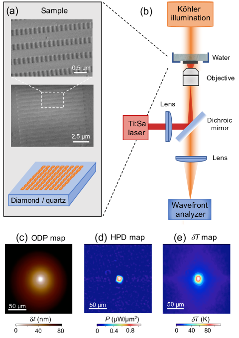
The heat source here consists of an array of gold nanoparticles illuminated at their plasmonic resonance wavelength Baffou and Quidant (2013); Baffou et al. (2013). We consider assemblies of gold cuboids with a thickness nm, a width nm, and a length ranging from nm to nm. As illustrated in Figure 1(a), the metallic cuboids are arranged in periodic two-dimensional rectangular patterns, each with constant cuboid dimensions and with a side-to-side distance of nm along the cuboid’s width direction and of along the cuboid’s length direction. These thermoplasmonic arrays were fabricated on two substrates, namely an ultrapure electronic grade diamond substrate grown by chemical vapor deposition (Element 6) and on a quartz substrate used as reference. The process combines an electron-beam lithography step, the deposition of 5 nm of titanium and 35 nm of gold, followed by a lift-off. Under continuous near-infrared laser illumination at their absorption resonance, the thermoplasmonic structures give rise to a delocalised temperature distribution, fairly uniform throughout the array Richardson et al. (2009); Baffou et al. (2013). The increase in temperature induced by the array is then governed, inter alia, by the absorption cross-section of each cuboids, the number of cuboids forming the array and the intensity of the infrared laser illumination.
Temperature variations induced by the thermoplasmonic structures were imaged using quadriwave lateral shearing interferometry Baffou et al. (2012) [see Fig. 1(b)]. This technique uses a wavefront analyser to indirectly provide temperature distributions with a diffraction-limited spatial resolution and an accuracy of about K. It relies on the temperature-dependent refractive index of a surrounding water layer covering the thermoplasmonic arrays. The heat generated by the arrays results in a steady-state temperature distribution, which provokes modifications of the refractive index in the water. These spatial variations in refractive index result in a wavefront distortion of a white light source illuminating the sample in a Köhler configuration. Such local distortions are recorded on a wavefront analyser, providing spatially-resolved optical path difference (OPD) maps. A typical OPD map recorded for a thermoplasmonic array deposited on quartz is shown in Figure 1(c). Post-processing of these data then enables retrieving the spatial distribution of the heat power density (HPD) [Fig. 1(d)] and of the spatial temperature variations [Fig. 1(e)]. This processing relies on a modeling of heat diffusion based on Green’s functions formalism Baffou et al. (2012).
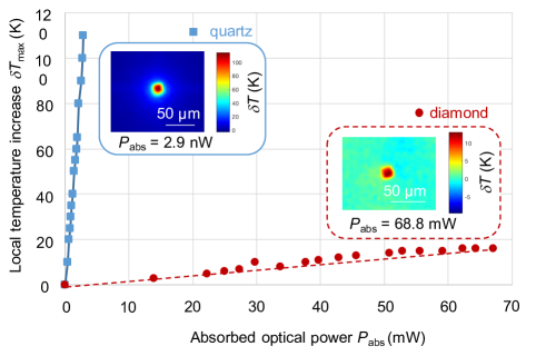
The plasmonic resonance wavelength of the heating structures varies both with the substrate and the shape of the metallic cuboids. In order to obtain a reliable comparison between the heat generated on an ultrapure diamond substrate and on a quartz substrate, experimental conditions leading to similar absorption cross-sections of the thermoplasmonic arrays were carefully selected. As explained in details in Ref. Baffou et al. (2012), the absorbed power can be inferred through a spatial integration of the HPD image. The absorption cross-section is then given by , where is the infrared laser intensity (power per unit area) and the number of cuboids forming the thermoplasmonic array. Similar absorption cross-sections nm2 were found for (i) nm2 cross-section cuboids illuminated at nm on the quartz substrate and for (ii) nm2 cross-section cuboids illuminated at nm on the diamond substrate.
With such experimental conditions, thermal images were recorded while increasing the absorbed infrared laser power . As shown in Figure 2, the maximum local heating evolves linearly with for both substrates, as expected. However, for equivalent absorption powers, the heating induced by the thermoplasmonic array on the quartz substrate is much higher than the one observed on diamond. A difference of two orders of magnitude is observed, with a maximum heating per absorbed power of K/mW and K/mW for quartz and diamond substrates, respectively. This discrepancy results from the large difference in thermal conductivity of the substrates. While is about W/(m.K) in quartz, it reaches values almost three-order of magnitudes higher in diamond with W/(m.K) depending on its purity. Consequently, while heat dissipation in quartz material is rather low, heat transfer in diamond is highly efficient. As such, the diamond substrate acts as a thermal sink that cools the heat source Setoura et al. (2013). Any architecture of thermal imagers based on bulk diamond will thus be perturbative: the measured temperature, though recorded with a high sensitivity, will be the temperature of the heat source however significantly cooled by the diamond substrate hosting the NV centers probes, down to temperatures that may be too small to be measured. This precludes the use of bulk diamond samples for wide-field thermal imaging.
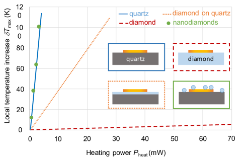
In order to reduce heat dissipation in bulk diamond, one alternative approach could be to rely on a thin diamond membrane bonded on a low thermal conductivity substrate, such as quartz. Figure 3 gathers finite-difference time-domain (FDTD) simulations based on heat conduction modeling of the temperature increase as a function of the heat power for three different diamond-based architectures: (i) a bulk diamond, (ii) a nm thin diamond membrane on quartz, and (iii) nanodiamonds dispersed on the heat source. The achieved temperature increase in the diamond-quartz heterostructure, is much higher than the one predicted for bulk diamond, and gets closer to the one expected on quartz. This stems from the strongly reduced effective thermal conductivity of the diamond-quartz heterostructure, in which the effective heat release through diamond occurs no longer in three but in two dimensions. In view of applications for thermal imaging, this partly lifts the limitations encountered with bulk diamond. However the heat diffusion throughout the diamond layer would still yield a lateral spreading of the temperature distribution over a length scale of few m’s, thus limiting the spatial resolution.
Conversely, the temperature of nanodiamonds exactly matches the one expected on the low thermal conductivity quartz substrate (see Fig. 3), with a homogenous temperature distribution across the entire nanodiamond volume. This thermalization of the nanodiamonds with the local thermal bath, combined with the constant temperature profile within the nanoparticle, allows for a non-perturbative measurement of the heat source temperature, despite the randomness in the position of the NV spin sensor inside the nanodiamond.
These results enable us to specify the optimal configuration for NV-based wide-field thermal imaging. Though bulk diamond imagers would provide the highest temperature sensitivity due to increased spin coherence times, efficient heat transfer in such high thermal conductivity material unavoidably lead to a significant cooling of the sample to be probed and thus prevents any effective temperature mapping at sub-micron scales. Engineered heterostructures stacking thin diamond membranes over low conductive substrates, feature significantly reduced heat diffusion, providing a valuable option for imaging at microscale. The most relevant configuration for non-invasive wide-field thermal imaging yet consists of random or ordered dispersions of diamond nanostructures on the hot sample to be probed. These thermal imagers may bring competitive imaging modalities with implications in the fields of micro- and nano-electronics, nanoplasmonics, or chemistry at nanoscale.
The authors acknowledge financial support from the French Research National Agency (through ANR THESEUS grant), from the center National de la Recherche Scientifique (through CNRS TEMPO grant) and from the European Commission (through H2020 program’s ASTERIQS, TSAR and ThermoQuant grants). This work was also partly supported by the french RENATECH network.
References
- Quintanilla and Liz-Marzand (2018) M. Quintanilla and L. M. Liz-Marzand, “Guiding rules for selecting a nanothermometer,” Nano Today 19, 126 (2018).
- Weng et al. (2018) Q. Weng, S. Komiyama, L. Yang, Z. An, P. Chen, S.-A. Biehs, Y. Kajihara, and W. Lu, “Imaging of nonlocal hot-electron energy dissipation via shot noise,” Science 360, 775 (2018).
- Li et al. (2018) L. Li, K. Liu, B. Suen, Q. Liu, and F. E. King, A.and Talke, “Numerical and experimental study of near-field heating using tip-enhanced raman spectroscopy (ters),” Tribol. Lett. 66, 26 (2018).
- Majundar (1999) A. Majundar, “Scanning thermal microscopy,” Annu. Rev. Mater. Sci. 29, 505–585 (1999).
- Gomes, Assy, and Chapuis (2015) S. Gomes, A. Assy, and P.-O. Chapuis, “Scanning thermal microscopy: A review,” physica status solidi (a) 212, 477–494 (2015).
- Halbertal et al. (2016) D. Halbertal, J. Cuppens, M. Ben Shalom, L. Embon, N. Shadmi, Y. Anahory, H. R. Naren, J. Sarkar, A. Uri, Y. Ronen, Y. Myasoedov, L. S. Levitov, E. Joselevich, A. K. Geim, and E. Zeldovn, “Nanoscale thermal imaging of dissipation in quantum systems,” Nature 539, 407–410 (2016).
- Aigouy et al. (2005) L. Aigouy, G. Tessier, M. Mortier, and B. Charlot, “Scanning thermal imaging of microelectronic circuits with a fluorescent nanoprobe,” Applied Physics Letters 87, 184105 (2005).
- Gruber et al. (1997) A. Gruber, A. Dräbenstedt, C. Tietz, L. Fleury, J. Wrachtrup, and C. V. Borczyskowski, “Scanning confocal optical microscopy and magnetic resonance on single defect centers,” Science 276, 2012–2014 (1997).
- Trusheim and Englund (2016) M. E. Trusheim and D. Englund, “Wide-field strain imaging with preferentially aligned nitrogen-vacancy centers in polycrystalline diamond,” New J. Phys. 18, 123023 (2016).
- Broadway et al. (2019) D. A. Broadway, B. C. Johnson, M. S. J. Barson, S. E. Lillie, N. Dontschuk, D. J. McCloskey, A. Tsai, T. Teraji, D. A. Simpson, A. Stacey, J. C. McCallum, J. E. Bradby, M. W. Doherty, L. C. L. Hollenberg, and J.-P. Tetienne, “Microscopic imaging of the stress tensor in diamond using in situ quantum sensors,” Nano Lett. 19, 4543–4550 (2019).
- Dolde et al. (2011) F. Dolde, H. Fedder, M. W. Doherty, T. Nöbauer, F. Rempp, G. Balasubramanian, T. Wolf, F. Reinhard, L. C. L. Hollenberg, F. Jelezko, and J. Wrachtrup, “Electric-field sensing using single diamond spins,” Nat. Phys 7, 459–463 (2011).
- Michl et al. (2019) J. Michl, J. Steiner, A. Denisenko, A. Bulau, A. Zimmermann, K. Nakamura, H. Sumiya, S. Onoda, P. Neumann, J. Isoya, and J. Wrachtrup, “Robust and accurate electric field sensing with solid state spin ensembles,” Nano Lett. 19, 4904–4910 (2019).
- Degen, Reinhard, and Cappellaro (2017) C. L. Degen, F. Reinhard, and P. Cappellaro, “Quantum sensing,” Rev. Mod. Phys. 89, 035002 (2017).
- Rondin et al. (2014) L. Rondin, J.-P. Tetienne, T. Hingant, J.-F. Roch, P. Maletinsky, and V. Jacques, “Magnetometry with nitrogen-vacancy defects in diamond,” Reports on Progress in Physics 77, 056503 (2014).
- Levine et al. (2019) E. V. Levine, M. J. Turner, P. Kehayias, C. A. Hart, N. Langellier, R. Trubko, D. R. Glenn, R. R. Fu, and R. L. Walsworth, “Principles and techniques of the quantum diamond microscope,” Nanophotonics (2019), 10.1515/nanoph-2019-0209.
- Kucsko et al. (2013) G. Kucsko, P. C. Maurer, N. Y. Yao, M. Kubo, H. J. Noh, P. K. Lo, H. Park, and M. D. Lukin, “Nanometre-scale thermometry in a living cell,” Nature 500, 54 (2013).
- Acosta et al. (2010) V. M. Acosta, E. Bauch, M. P. Ledbetter, A. Waxman, L.-S. Bouchard, and D. Budker, “Temperature dependence of the nitrogen-vacancy magnetic resonance in diamond,” Phys. Rev. Lett. 104, 070801 (2010).
- Neumann et al. (2013) P. Neumann, I. Jakobi, F. Dolde, C. Burk, R. Reuter, G. Waldherr, J. Honert, T. Wolf, A. Brunner, J. H. Shim, D. Suter, H. Sumiya, J. Isoya, and J. Wrachtrup, “High-precision nanoscale temperature sensing using single defects in diamond,” Nano Letters 13, 2738–2742 (2013).
- Wang et al. (2015) J. Wang, F. Feng, J. Zhang, J. Chen, Z. Zheng, L. Guo, W. Zhang, X. Song, G. Guo, L. Fan, C. Zou, L. Lou, W. Zhu, and G. Wang, “High-sensitivity temperature sensing using an implanted single nitrogen-vacancy center array in diamond,” Phys. Rev. B 91, 155404 (2015).
- Toyli et al. (2013) D. M. Toyli, C. F. de las Casas, D. J. Christle, V. V. Dobrovitski, and D. D. Awschalom, “Fluorescence thermometry enhanced by the quantum coherence of single spins in diamond,” Proceedings of the National Academy of Sciences 110, 8417–8421 (2013), https://www.pnas.org/content/110/21/8417.full.pdf .
- Tran et al. (2019) T. T. Tran, B. Regan, E. A. Ekimov, Z. Mu, Y. Zhou, W. Gao, P. Narang, A. S. Solntsev, M. Toth, I. Aharonovich, and C. Bradac, “Anti-stokes excitation of solid-state quantum emitters for nanoscale thermometry,” Science Advances 5, eaav9180 (2019).
- Plakhotnik et al. (2014) T. Plakhotnik, M. W. Doherty, J. H. Cole, R. Chapman, and N. B. Manson, “All-optical thermometry and thermal properties of the optically detected spin resonances of the nv?center in nanodiamond,” Nano Letters 14, 4989 (2014).
- Nguyen et al. (2018) C. T. Nguyen, R. E. Evans, A. Sipahigil, M. K. Bhaskar, D. D. Sukachev, V. N. Agafonov, V. A. Davydov, L. F. Kulikova, F. Jelezko, and M. D. Lukin, “All-optical nanoscale thermometry with silicon-vacancy centers in diamond,” Appl. Phys. Lett. 112, 203102 (2018).
- Fan et al. (2018) J.-W. Fan, I. Cojocaru, J. Becker, I. V. Fedotov, M. H. A. Alkahtani, A. Alajlan, S. Blakley, M. Rezaee, A. Lyamkina, Y. N. Palyanov, Y. M. Borzdov, Y.-P. Yang, A. Zheltikov, P. Hemmer, and A. V. Akimov, “Germanium-vacancy color center in diamond as a temperature sensor,” ACS Photonics 5, 765 (2018).
- Alkahtani et al. (2018) M. Alkahtani, I. Cojocaru, X. Liu, T. Herzig, J. Meijer, J. Kupper, T. Luhmann, A. V. Akimov, and P. R. Hemmer, “Tin-vacancy in diamonds for luminescent thermometry,” Appl. Phys. Lett. 112, 241902 (2018).
- Wang et al. (2018) N. Wang, G.-Q. Liu, W.-H. Leong, H. Zeng, X. Feng, S.-H. Li, F. Dolde, H. Fedder, J. Wrachtrup, X.-D. Cui, S. Yang, Q. Li, and R.-B. Liu, “Magnetic criticality enhanced hybrid nanodiamond thermometer under ambient conditions,” Phys. Rev. X 8, 011042 (2018).
- Liu et al. (2019) C.-F. Liu, W.-H. Leong, K. Xia, X. Feng, A. Finkler, A. Denisenko, J. Wrachtrup, A. Li, and R.-B. Liu, “Ultra-sensitive hybrid diamond nanothermometer,” (2019), arXiv:1912.12097 [quant-ph] .
- Fedotov et al. (2014) I. V. Fedotov, S. Blakley, E. E. Serebryannikov, N. A. Safronov, V. L. Velichansky, M. O. Scully, and A. M. Zheltikov, “Fiber-based thermometry using optically detected magnetic resonance,” Applied Physics Letters 105, 261109 (2014), https://doi.org/10.1063/1.4904798 .
- Laraoui et al. (2015) A. Laraoui, H. Aycock-Rizzo, Y. Gao, X. Lu, E. Riedo, and C. A. Meriles, “Imaging thermal conductivity with nanoscale resolution using a scanning spin probe,” Nature Communications 6, 8954 (2015).
- Tetienne et al. (2016) J.-P. Tetienne, A. Lombard, D. A. Simpson, C. Ritchie, J. Lu, P. Mulvaney, and L. C. L. Hollenberg, “Scanning nanospin ensemble microscope for nanoscale magnetic and thermal imaging,” Nano Letters 16, 326–333 (2016).
- Andrich et al. (2018) P. Andrich, J. Li, X. Liu, F. J. Heremans, P. F. Nealey, and D. D. Awschalom, “Microscale-resolution thermal mapping using a flexible platform of patterned quantum sensors,” Nano Letters 18, 4684–4690 (2018).
- Baffou and Quidant (2013) G. Baffou and R. Quidant, “Thermo-plasmonics: using metallic nanostructures as nano-sources of heat,” Laser & Photonics Reviews 7, 171–187 (2013).
- Baffou et al. (2013) G. Baffou, P. Berto, E. Bermudez Urena, R. Quidant, S. Monneret, J. Polleux, and H. Rigneault, “Photoinduced heating of nanoparticle arrays,” ACS Nano 7, 6478–6488 (2013).
- Richardson et al. (2009) H. H. Richardson, M. T. Carlson, P. J. Tandler, P. Hernandez, and A. O. Govorov, “Experimental and theoretical studies of light-to-heat conversion and collective heating effects in metal nanoparticle solutions,” Nano Letters 9, 1139–1146 (2009).
- Baffou et al. (2012) G. Baffou, P. Bon, J. Savatier, J. Polleux, M. Zhu, M. Merlin, H. Rigneault, and S. Monneret, “Thermal imaging of nanostructures by quantitative optical phase analysis,” ACS Nano 6, 2452–2458 (2012).
- Setoura et al. (2013) K. Setoura, Y. Okada, D. Werner, and S. Hashimoto, “Observation of nanoscale cooling effects by substrates and the surrounding media for single gold nanoparticles under cw-laser illumination,” ACS Nano 7, 7874–7885 (2013).