Photon-assisted tunneling at the atomic scale: Probing resonant Andreev reflections from Yu-Shiba-Rusinov states
Abstract
Tunneling across superconducting junctions proceeds by a rich variety of processes, which transfer single electrons, Cooper pairs, or even larger numbers of electrons by multiple Andreev reflections. Photon-assisted tunneling combined with the venerable Tien-Gordon model has long been a powerful tool to identify tunneling processes between superconductors. Here, we probe superconducting tunnel junctions including an impurity-induced Yu-Shiba-Rusinov (YSR) state by exposing a scanning tunneling microscope with a superconducting tip to microwave radiation. We find that a simple Tien-Gordon description describes tunneling of single electrons and Cooper pairs into the bare substrate, but breaks down for tunneling via YSR states by resonant Andreev reflections. We develop an improved theoretical description which is in excellent agreement with the data. Our results establish photon-assisted tunneling as a powerful tool to analyze tunneling processes at the atomic scale which should be particularly informative for unconventional and topological superconductors.
Subgap states in superconductors Balatsky et al. (2006); Heinrich et al. (2018); Sauls (2018); Lutchyn et al. (2018) provide a local probe of interactions competing with superconductivity Deacon et al. (2010); Franke et al. (2011); Lee et al. (2014); Jellinggaard et al. (2016); Lee et al. (2017); Schneider et al. (2019); Liebhaber et al. (2020) and govern the Josephson coupling in superconducting junctions Bretheau et al. (2013). They also provide promising arenas for quantum computing applications, owing to protection by the quasiparticle gap Zazunov et al. (2003); Chtchelkatchev and Nazarov (2003); Janvier et al. (2015) or by topology Kitaev (2001). A wealth of information can thus be obtained from tunneling experiments on subgap states. The differential conductance reveals the energy of the bound states Yazdani et al. (1997); Ji et al. (2008), spatially resolves electron and hole components of bound state wavefunctions in scanning tunneling microscopy Ménard et al. (2015); Choi et al. (2017), and provides access to inelastic relaxation rates underlying quasiparticle poisoning Ruby et al. (2015a); Albrecht et al. (2017). In recent years, this has been instrumental in attempts to distinguish Majorana from Andreev and Yu-Shiba-Rusinov (YSR) states Lutchyn et al. (2018).
Reliably extracting this information requires a microscopic understanding of the tunneling mechanism. Indeed, tunneling across superconducting junctions proceeds by a remarkably rich variety of processes. As single-electron tunneling requires sufficient energy to excite quasiparticles in the superconducting source and drain, transport at low energies is dominated by multi-electron processes including Cooper pair tunneling near zero bias Josephson (1962); Naaman et al. (2001) and multi-electron tunneling via (multiple) Andreev reflections at higher subgap biases Schrieffer and Wilkins (1963); Taylor and Burstein (1963); Andreev (1964); Ternes et al. (2006). Unlike standard differential conductance measurements, photon-assisted tunneling directly reveals the effective charge of the transferred carriers through the sideband spacings in the bias voltage as well as in the amplitude of the high-frequency (HF) radiation Tien and Gordon (1963); Falci et al. (1991); Roychowdhury et al. (2015).
Here, we provide direct evidence for various tunneling mechanisms at the atomic scale by exposing a scanning tunneling microscope (STM) to high-frequency radiation. We first use photon-assisted tunneling from a superconducting tip into a pristine superconducting substrate to identify single-electron tunneling both above and within the superconducting gap, as well as Cooper-pair tunneling and Andreev reflections at subgap voltages. We then exploit the resolution and the tunability of the junction conductance afforded by an STM to unravel charge transfer processes in the presence of atomic-scale structures Ruby et al. (2015a); Randeria et al. (2016); Farinacci et al. (2018); Brand et al. (2018). We demonstrate this capability by investigating resonant tunneling via YSR states of individual magnetic adatoms. Remarkably, we observe that in the presence of subgap states, photon-assisted Andreev reflections exhibit distinct deviations from standard Tien-Gordon theory. Our more elaborate theory explains these deviations and shows how they encode properties of the subgap states as well as the underlying tunneling processes, including the transferred charge.
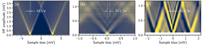
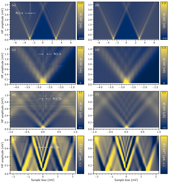
For our experiments, we implemented a high-frequency (HF) circuit into our STM setup at 1.3 K with the final cable terminating close to the STM junction and acting as an efficient HF antenna [see Supplementary Information (SI)]. We use a superconducting Pb-coated tungsten tip facing a Pb(111) or Pb(110) surface. At large junction resistance, tunneling occurs beyond a threshold voltage of , where single-electron tunneling becomes possible and excites one quasiparticle each in tip and substrate. In the presence of 40-GHz radiation, the resulting Bardeen-Cooper-Schrieffer (BCS) coherence peaks in the differential conductance dd split into symmetric sidebands with distinct maxima spaced by (Fig. 1a). Electrons can emit or absorb photons while tunneling, so that the threshold voltages follow from . The photon sidebands are observable within a V-shaped region as a function of bias voltage and HF amplitude (Fig. 1a), as the number of photons is limited by the maximal energy which the tunneling electron can exchange with the radiation field. The separation of sidebands is direct evidence for single-electron tunneling.
A quantitative understanding is provided by the Tien-Gordon model which includes the HF radiation as an additional voltage applied to the junction Tien and Gordon (1963). Including the resulting modulation of the energy levels in the electrodes predicts differential conductance sidebands
| (1) |
The strength of the th sideband involves the Bessel function and denotes dd in the absence of HF radiation. Here, we have already generalized the Tien-Gordon formula to the case that electrons are transferred in an elementary tunneling process Falci et al. (1991). Using Eq. (1) for single-electron tunneling () with the data in the absence of the HF radiation as input, we find excellent agreement with our experimental results (see SI).
Unlike single-electron tunneling, Cooper-pair tunneling does not excite tip or substrate and can thus be observed as a zero-bias Josephson peak once the junction conductance is sufficiently large. The radiation field also splits the Josephson peak into a distinct V-shaped structure of resonant sidebands (Fig. 1b, see also Roychowdhury et al. (2015)). The sideband spacings in bias voltage and in HF amplitude are now , corresponding to half the value observed for the BCS coherence peaks. This is consistent with as expected for electron pairs and thus provides direct evidence for Cooper-pair tunneling. Indeed, simulations based on Eq. (1) with are in excellent agreement with the experimental maps (see SI).
To further substantiate our ability to determine the elementary charge carriers in superconducting STM junctions, we investigate Andreev reflections in the HF field Chauvin et al. (2006). The first Andreev reflection can be resolved at for sufficiently high junction conductance ( in Fig. 1c). This dd peak emerges from the transfer of a Cooper pair into the substrate, leaving two quasiparticles behind in the tip, and a corresponding process generating quasiparticles in the substrate. The radiation field splits the Andreev reflection peaks into V-shaped patterns similar to those of the Josephson peak. (Note that we show for better resolution.) We find a sideband spacing of , equal to , revealing the underlying charge transfer of (see Fig. 2a for a sketch of the process leading to the first sideband).
The Tien-Gordon approach as embodied by Eq. (1) is thus highly successful at describing photon-assisted tunneling between tip and bulk superconducting substrate, directly revealing the number of electrons involved in the elementary tunneling process. We now extend the technique to tunneling into YSR states induced by magnetic adatoms. Remarkably, we find that in general, Eq. (1) breaks down for tunneling into subgap states and has to be replaced by a more elaborate description.
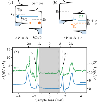
We induce YSR states by depositing Mn atoms on a Pb(111) surface. Mn atoms have been shown to remain stable when approached by the tip, with the junction conductance changing over several orders of magnitude Ruby et al. (2015a). Differential conductance spectra recorded on the Mn atoms reveal several YSR states (Fig. 2c, blue) at bias voltages , with YSR-state energies . These can be understood as a multiplet of orbitals with its degeneracy partially lifted by the local crystal field Ruby et al. (2016). Here, we focus on the most intense YSR resonance at . While the position of the resonance, labeled as , remains unchanged when approaching the adatom with the STM tip and changing the junction conductance by three orders of magnitude, the relative magnitude of the resonances at positive and negative bias changes and eventually inverts (see Fig. 2c and extracted intensities in SI). The inversion reflects a transition from dominant single-electron tunneling at large tip distances (Fig. 2c, green) to dominant Andreev processes at small distances (Fig. 2c, blue) and manifests the asymmetry between the electron wave function and hole wavefunction of the YSR state, Ruby et al. (2015a).
Measured dd maps of photon-assisted tunneling through Pb–Mn–Pb junctions are shown in Fig. 3a and b and exhibit clear deviations from the Tien-Gordon expression in Eq. (1). At high junction conductances (Fig. 3b), the maps still resemble a V-shaped pattern for positive bias voltages, but are distinctly different for negative biases. Most strikingly, the V-shaped pattern gives way to a Y-shaped form, which resembles none of the maps for the unstructured surface. Even for positive bias voltages with its V-shaped pattern, the data are surprising. While tunneling at these junction conductances is dominated by Andreev reflections and thus transfers electron pairs Ruby et al. (2015a), the periods of the intensity modulations seemingly indicate single-electron tunneling.
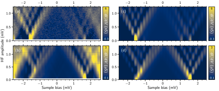
These unexpected results contrast with dd maps at lower junction conductance (Fig. 3a), which show V-shaped patterns centered at for both bias polarities. Moreover, the observed period of the intensity modulations is consistent with the expectation Ruby et al. (2015a) that tunneling is dominated by individual electrons which leave behind a quasiparticle in the tip and occupy the YSR state at energy [see Fig. 2b, with a similar hole process for )]. With the corresponding thresholds for photon-assisted tunneling, we apply the Tien-Gordon model to the individual tunneling rates and obtain
| (2) |
for electrons of energy in the substrate. Here, is the tunneling rate in the absence of radiation (see SI for details). At these low junction conductances, inelastic processes in the substrate (with rate , see Fig. 2b) empty the YSR state long before the next tunneling event, so that tunneling is the rate-limiting step. The current can then be computed by integrating the tunneling rate (2) and a corresponding hole rate with appropriate thermal occupation factors. (For the full expressions, see SI.) The result in Fig. 3c exhibits excellent agreement with our data in Fig. 3a. In particular, the calculation also reproduces a second V-shaped structure centered at which originates from thermally activated quasiparticles Ruby et al. (2015a) (see also SI). Unlike our simulations for unstructured substrates, these simulations use only the YSR asymmetry and relaxation rates as derived from experiment as input, providing strong confirmation for the interpretation of the underlying processes.
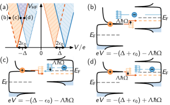
At larger junction conductances, inelastic relaxation out of the YSR state becomes slower than electron and hole tunneling across the junction. Tunneling is then dominated by resonant Andreev reflections. Focusing first on negative bias voltages near , this process involves hole tunneling into the negative-energy YSR state, electron tunneling out of the positive energy YSR state, and breaking of a Cooper pair in the substrate (Fig. 2b). The resonant nature of this process has two important implications. First, Andreev reflection from YSR states is much stronger than from unstructured substrates. Second, there are separate thresholds for electron and hole tunneling. The condition for holes is complemented by for electrons (see Fig. 4 for illustration and representative processes). Without HF radiation, the electron process is automatically above threshold when the hole process is. But with HF radiation, this is in general no longer the case.
As a result of the maximal number of absorbed or emitted photons, the separate thresholds define two distinct V-shaped regions at negative biases, one for holes, (left red V in Fig. 4a), and another one for electrons, (left blue V in Fig. 4a). Resonant Andreev reflection takes place when electron and hole processes are both above threshold, so that only the outer (red) V-shaped region appears in experiment. The Y shape results from the strongly asymmetric electron and hole amplitudes of the YSR state, . Due to this asymmetry, the hole tunneling rate is generically significantly larger than the electron rate . Thus, electron tunneling is, roughly speaking, the rate-limiting step governing the tunneling current, and features due to are much more pronounced. This explains why sidebands appear with high intensity in regions where the two V shapes overlap and why the observed maxima remain spaced by despite the underlying two-electron tunneling. The thresholds for the hole processes still contribute to the low-voltage arm of the Y (full red line in Fig. 4a). Here, hole tunneling just sets in and is comparable in rate to electron tunneling. Thus, in this region, hole thresholds are visible in addition to electron thresholds, resulting in the prominent double structure of the low-voltage arm of the Y shape observed in Fig. 3b (see SI for more details). The results of a full theory of resonant Andreev reflections, which properly treats it as a single coherent process involving both electron and hole tunneling, are shown in Fig. 3d. Using only few experimental parameters as input, we find excellent agreement with our data, reproducing the Y shape including the double structure as well as the sideband spacing (see SI for details).
At positive bias, the outer V shape, centered at (blue in Fig. 4a), emerges from the electron condition, and the inner one around (red) from the hole condition. Again, structure is only visible within the outer (blue) V shape where both electron and hole processes are above threshold. But the ‘rate-limiting’ electron tunneling is now associated with the outer (blue) V shape. Consequently, pronounced sidebands appear within the entire outer V shape, again spaced by . These observations are also nicely reproduced by our theoretical calculations of the resonant Andreev reflections in Fig. 3d. We finally emphasize that the inner V shapes at large junction conductance should not be confused with the thermal processes at low junction conductance. Thermal processes require inelastic relaxation and are therefore much weaker than resonant Andreev reflections at large junction conductance.
In conclusion, exposing a scanning tunneling microscope with a superconducting tip to high-frequency radiation constitutes a powerful tool to investigate the subgap structure of superconducting substrates with atomic resolution. Here, we have established this ability for YSR states and showed that the data provide a comprehensive picture of the tunneling process. Exploiting the tunability of the junction conductance over several orders of magnitude, we have specifically obtained exquisite insight into the contributions of Andreev processes to subgap tunneling.
Such Andreev processes should provide a particularly revealing window into the physics of unconventional and topological superconductors, making atomic-resolution photon-assisted tunneling highly promising for such systems. For instance, strongly disordered superconducting films are believed to exhibit a transition from a pseudogap regime with preformed Cooper pairs into a superconducting phase with long-range phase coherence Dubouchet et al. (2019). Spatially resolved photon-assisted tunneling promises detailed information on the nature of subgap tunneling processes, their spatial variation, and hence the nature of pairing correlations. As a second example, resonant Andreev reflections underlie tunneling experiments probing putative Majorana modes Law et al. (2009); Flensberg (2010), for instance in chains of magnetic adatoms on -wave superconductors Nadj-Perge et al. (2014); Ruby et al. (2015b); Pawlak et al. (2016); Feldman et al. (2017); Jeon et al. (2017); Kim et al. (2018). Photon-assisted tunneling can not only ascertain the nature of the tunneling processes, but also serve to distinguish true zero-energy states from states with a small, but finite energy . In fact, finite-energy states with electron and hole wave functions of the same order exhibit splittings due to the separate electron and hole thresholds which should be detectable with high resolution due to their large multiplicity throughout the -shaped region.
Acknowledgements.
We thank K. Flensberg for fruitful discussions and C. Lotze for technical support. We gratefully acknowledge funding by the European Research Council under the Consolidator Grant "NanoSpin", by Deutsche Forschungsgemeinschaft and Agence National de Recherche under grant "JOSPEC", and by CRCs 183 and 910 of Deutsche Forschungsgemeinschaft.References
- Balatsky et al. (2006) A. V. Balatsky, I. Vekhter, and J. X. Zhu, Rev. Mod. Phys. 78, 373 (2006).
- Heinrich et al. (2018) B. W. Heinrich, J. I. Pascual, and K. J. Franke, Prog. Surf. Sci. 93, 1 (2018).
- Sauls (2018) J. A. Sauls, Phil. Trans.R. Soc. A 376, 20180140 (2018).
- Lutchyn et al. (2018) R. M. Lutchyn, E. P. A. M. Bakkers, L. P. Kouwenhoven, P. Krogstrup, C. M. Marcus, and Y. Oreg, Nature Rev. Mat. 3, 52 (2018).
- Deacon et al. (2010) R. S. Deacon, Y. Tanaka, A. Oiwa, R. Sakano, K. Yoshida, K. Shibata, K. Hirakawa, and S. Tarucha, Phys. Rev. Lett. 104, 076805 (2010).
- Franke et al. (2011) K. J. Franke, G. Schulze, and J. I. Pascual, Science 332, 940 (2011).
- Lee et al. (2014) E. J. Lee, X. Jiang, M. Houzet, R. Aguado, C. M. Lieber, and S. De Franceschi, Nat. Nanotechnol. 9, 79 (2014).
- Jellinggaard et al. (2016) A. Jellinggaard, K. Grove-Rasmussen, M. H. Madsen, and J. Nygård, Phys. Rev. B 94, 064520 (2016).
- Lee et al. (2017) E. J. H. Lee, X. Jiang, R. itko, R. Aguado, C. M. Lieber, and S. De Franceschi, Phys. Rev. B 95, 180502 (2017).
- Schneider et al. (2019) L. Schneider, M. Steinbrecher, L. Rózsa, J. Bouaziz, K. Palotás, M. dos Santos Dias, J. Wiebe, and R. Wiesendanger, npj Quantum Materials 4, 42 (2019).
- Liebhaber et al. (2020) E. Liebhaber, S. Acero González, R. Baba, G. Reecht, B. W. Heinrich, S. Rohlf, K. Rossnagel, F. von Oppen, and K. J. Franke, Nano Letters 20, 339 (2020).
- Bretheau et al. (2013) L. Bretheau, Ç. Ö. Girit, H. Pothier, D. Esteve, and C. Urbina, Nature 499, 312 (2013).
- Zazunov et al. (2003) A. Zazunov, V. S. Shumeiko, E. N. Bratus’, J. Lantz, and G. Wendin, Phys. Rev. Lett. 90, 087003 (2003).
- Chtchelkatchev and Nazarov (2003) N. M. Chtchelkatchev and Y. V. Nazarov, Phys. Rev. Lett. 90, 226806 (2003).
- Janvier et al. (2015) C. Janvier, L. Tosi, L. Bretheau, Ç. Ö. Girit, M. Stern, P. Bertet, P. Joyez, D. Vion, D. Esteve, M. F. Goffman, H. Pothier, and C. Urbina, Science 349, 1199 (2015).
- Kitaev (2001) A. Y. Kitaev, Physics Uspekhi 44, 131 (2001).
- Yazdani et al. (1997) A. Yazdani, B. A. Jones, C. P. Lutz, M. F. Crommie, and D. M. Eigler, Science 275, 1767 (1997).
- Ji et al. (2008) S.-H. Ji, T. Zhang, Y.-S. Fu, X. Chen, X.-C. Ma, J. Li, W.-H. Duan, J.-F. Jia, and Q.-K. Xue, Phys. Rev. Lett. 100, 226801 (2008).
- Ménard et al. (2015) G. C. Ménard, S. Guissart, C. Brun, S. Pons, V. S. Stolyarov, F. Debontridder, M. V. Leclerc, E. Janod, L. Cario, D. Roditchev, P. Simon, and T. Cren, Nature Phys. 11, 1013 (2015).
- Choi et al. (2017) D.-J. Choi, C. Rubio-Verdú, J. De Bruijckere, M. M. Ugeda, N. Lorente, and J. I. Pascual, Nature Commun. 8, 15175 (2017).
- Ruby et al. (2015a) M. Ruby, F. Pientka, Y. Peng, F. von Oppen, B. W. Heinrich, and K. J. Franke, Phys. Rev. Lett. 115, 087001 (2015a).
- Albrecht et al. (2017) S. M. Albrecht, E. B. Hansen, A. P. Higginbotham, F. Kuemmeth, T. S. Jespersen, J. Nygård, P. Krogstrup, J. Danon, K. Flensberg, and C. M. Marcus, Phys. Rev. Lett. 118, 137701 (2017).
- Josephson (1962) B. Josephson, Physics Letters 1, 251 (1962).
- Naaman et al. (2001) O. Naaman, W. Teizer, and R. C. Dynes, Phys. Rev. Lett. 87, 097004 (2001).
- Schrieffer and Wilkins (1963) J. R. Schrieffer and J. W. Wilkins, Phys. Rev. Lett. 10, 17 (1963).
- Taylor and Burstein (1963) B. N. Taylor and E. Burstein, Phys. Rev. Lett. 10, 14 (1963).
- Andreev (1964) A. F. Andreev, Sov. Phys. JETP 19, 1228 (1964).
- Ternes et al. (2006) M. Ternes, W. D. Schneider, J. C. Cuevas, C. P. Lutz, C. F. Hirjibehedin, and A. J. Heinrich, Phys. Rev. B 74, 132501 (2006).
- Tien and Gordon (1963) P. K. Tien and J. P. Gordon, Phys. Rev. 129, 647 (1963).
- Falci et al. (1991) G. Falci, V. Bubanja, and G. Schön, Z. Phys. B 85, 451 (1991).
- Roychowdhury et al. (2015) A. Roychowdhury, M. Dreyer, J. R. Anderson, C. J. Lobb, and F. C. Wellstood, Phys. Rev. Appl. 4 (2015).
- Randeria et al. (2016) M. T. Randeria, B. E. Feldman, I. K. Drozdov, and A. Yazdani, Phys. Rev. B 93, 161115 (2016).
- Farinacci et al. (2018) L. Farinacci, G. Ahmadi, G. Reecht, M. Ruby, N. Bogdanoff, O. Peters, B. W. Heinrich, F. von Oppen, and K. J. Franke, Phys. Rev. Lett. 121, 196803 (2018).
- Brand et al. (2018) J. Brand, S. Gozdzik, N. Néel, J. L. Lado, J. Fernández-Rossier, and J. Kröger, Phys. Rev. B 97, 195429 (2018).
- Chauvin et al. (2006) M. Chauvin, P. vom Stein, H. Pothier, P. Joyez, M. E. Huber, D. Esteve, and C. Urbina, Phys. Rev. Lett. 97, 067006 (2006).
- Ruby et al. (2016) M. Ruby, Y. Peng, F. von Oppen, B. W. Heinrich, and K. J. Franke, Phys. Rev. Lett. 117, 186801 (2016).
- Dubouchet et al. (2019) T. Dubouchet, B. Sacépé, J. Seidemann, D. Shahar, M. Sanquer, and C. Chapelier, Nat. Phys. 15, 233 (2019).
- Law et al. (2009) K. T. Law, P. A. Lee, and T. K. Ng, Phys. Rev. Lett. 103, 237001 (2009).
- Flensberg (2010) K. Flensberg, Phys. Rev. B 82, 180516 (2010).
- Nadj-Perge et al. (2014) S. Nadj-Perge, I. K. Drozdov, J. Li, H. Chen, S. Jeon, J. Seo, A. H. MacDonald, B. A. Bernevig, and A. Yazdani, Science 346, 602 (2014).
- Ruby et al. (2015b) M. Ruby, F. Pientka, Y. Peng, F. von Oppen, B. W. Heinrich, and K. J. Franke, Phys. Rev. Lett. 115, 197204 (2015b).
- Pawlak et al. (2016) R. Pawlak, M. Kisiel, J. A. Klinovaja, T. Meier, S. Kawai, T. Glatzel, D. Loss, and E. Meyer, npj Quantum Inf. 2, 16035 (2016).
- Feldman et al. (2017) B. E. Feldman, M. T. Randeria, J. Li, S. Jeon, Y. Xie, Z. Wang, I. K. Drozdov, B. Andrei Bernevig, and A. Yazdani, Nat. Phys. 13, 286 (2017).
- Jeon et al. (2017) S. Jeon, Y. Xie, J. Li, Z. Wang, B. A. Bernevig, and A. Yazdani, Science 358, 772 (2017).
- Kim et al. (2018) H. Kim, A. Palacio-Morales, T. Posske, L. Rózsa, K. Palotás, L. Szunyogh, M. Thorwart, and R. Wiesendanger, Science Advances 4, eaar5251 (2018).
Supplementary Information
S1 Experimental Details
S1.1 Implementation of high-frequency circuit
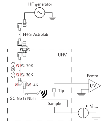
Exposing a scanning tunneling microscope (STM) to high-frequency (HF) radiation in the GHz range requires a dedicated circuit Baumann et al. (2015); Natterer et al. (2019); Friedlein et al. (2019); Seifert et al. (2020). Typical cables in low-temperature STMs are designed for efficient filtering of environmental radiation, which would otherwise induce noise in the tunneling junction. Thus, high-frequency signals require separate cables, which transmit the signal without compromising other stability and resolution criteria of the STM.
We have designed a circuit in parallel to the STM cables. A sketch of the setup is shown in Fig. S1. The HF signal from a signal generator (R&S® SMB 100A) is transmitted to the chamber via a semi-flexible cable (H+S Astrolab KK-SF240-2X11SK, ). All connectors outside and inside the chamber as well as the feedthrough (Allectra 242-SMAD40G-C16) are designed as SMK , suited for frequencies up to . Inside the UHV chamber, a silver-plated beryllium-copper coaxial cable (SC-219/50-SB-B, ) is passed through the cryostat and attached to the cryostat’s radiation shields. At the bottom of the -plate of the croystat it is connected (via SMK connectors) to a superconducting niobium titanate (NbTi) coaxial cable (SC-086/50-NbTi-NbTi, ), which has negligible attenuation losses at low temperature. This cable terminates close to the STM junction with the outer conductor being removed over a length of and bent up .
S1.2 Characterization of HF circuit
The HF signal applied to the antenna effectively modulates the bias voltage across the STM junction. When we applied the minimum output signal, i.e., of our signal generator (R&S® SMB 100A), the superconducting energy gap completely vanished, reflecting an effective bias voltage modulation of several mV. For lower bias-voltage modulations, we inserted a attenuator at the output of the signal generator. To characterize the HF radiation arriving at the STM junction, we make use of the highly nonlinear current-voltage characteristics of a superconductor-superconductor tunneling junction. A similar scheme can be used at other nonlinearities such as inelastic spin excitations Baumann et al. (2015).
We set the bias voltage close to the nonlinearity in the current-voltage characteristic . In the case of a Pb–Pb junction, we applied , which is just below the onset of quasiparticle tunneling across the superconductor–superconductor junction at . We then switch on the HF radiation (see sketch in Fig. S2a) and measure the time-averaged current as a function of applied HF power (Fig. S2b). We determine the damping by fitting the experimental time-averaged current to
| (S1) |
where is the damping, is the power of the source in dBm and is its impedance. Here, we use that the power level in dBm can be converted to conventional units by (mW)= mW. The extracted damping is shown in Fig. S2c.
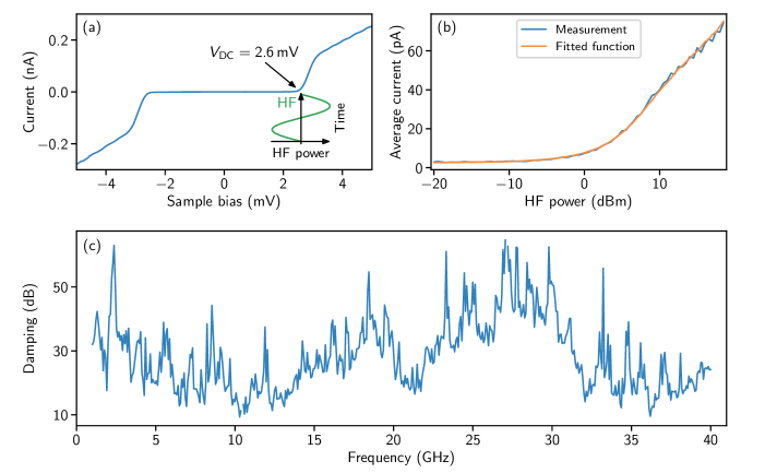
Alternatively, the effective radiation power at the STM junction can be determined by comparison with Tien-Gordon theory. The -shaped splitting of, e.g., the BCS coherence peaks in the power-dependent dd maps provides an accurate measure of the radiation power that leads to photon-assisted tunneling (see main text). This method is very efficient for specific frequencies, but would be rather time consuming for a full frequency-dependent characterization of the HF circuit. We used the method to monitor variations of the damping properties over the timescale of the measurements for the presented experiments at a constant frequency of .
S1.3 Experimental parameters
Table S1 collects the experimental parameters at which the measurements presented in the figures, both in the main text and the supplementary, were taken.
S2 Theoretical considerations
Here, we present theoretical considerations on photon-assisted tunneling in superconductor-superconductor junctions. We begin with a brief summary of photon-assisted tunneling from a superconducting tip into a pristine superconducting substrate, including the three processes for which we show experimental data in the main text: (i) single-electron tunneling at (coherence peaks), (ii) Andreev reflections at , and (iii) the Josephson peak at . We will use a Fermi-golden-rule approach for all three of these processes. This then provides the background for a discussion of photon-assisted resonant Andreev reflections through Yu-Shiba-Rusinov (YSR) states.
S2.1 General formulation
Tunneling from a superconducting tip with Hamiltonian into a superconducting substrate with Hamiltonian is described by the tunneling Hamiltonian
| (S2) |
where denotes the electron creation operators at position and with spin in the tip () or the substrate (). The position of the tip is denoted by . The overall Hamiltonian
| (S3) |
conserves the total number of particles . The bias voltage between tip and substrate is included through different chemical potentials and for tip and substrate,
| (S4) |
and consists of an applied voltage as well as an voltage,
| (S5) |
The voltage is generated by the radiation field of frequency Tien and Gordon (1963).
The BCS descriptions of the superconducting tip and substrate start from the grand-canonical Hamiltonians and , which measure the single-particle energies in tip and substrate from the respective chemical potentials and . This makes it useful to perform the time-dependent canonical transformation
| (S6) |
which transforms the Hamiltonian (S3) into , i.e.,
| (S7) |
Here we used that and conserve and , so that . In contrast, the tunneling Hamiltonian only conserves the total number of electrons , but not and separately. This makes the transformed tunneling Hamiltonian time dependent,
| (S8) |
where the time-dependent phase
| (S9) |
includes the effects of the applied bias voltage.
The transformed Hamiltonian can now be treated within BCS mean field approximation, so that the unperturbed Hamiltonian becomes
| (S10) |
Here, denotes the normal-state dispersion, the superconducting gap is taken to be identical for tip and substrate, and we temporarily assume a pristine substrate without magnetic adatom.
S2.2 Tunneling into pristine superconductors
S2.2.1 Coherence peaks
Single-electron tunneling across a superconducting junction creates a quasiparticle each in source and drain electrode in the final state and consequently requires a threshold voltage of . The resulting coherence peaks are split into sidebands by the radiation field. To obtain these sidebands, we expand the time-dependent phase factor appearing in the tunneling Hamiltonian into a Fourier series,
| (S11) |
with the coefficients involving the Bessel functions . Assuming that temperature is small compared to the superconducting gap, tunneling only occurs from source to drain, and Fermi’s golden rule gives
| (S12) |
for the tunneling current. Here, we have expressed the electron operators in terms of Bogoliubov quasiparticle operators in the usual way, and denote the familiar electron and hole quasiparticle wavefunctions in BCS theory, and is the quasiparticle energy. (We assume identical superconductors for tip and substrate, as is the case in the experiment.) The prefactor of two accounts for spin. Thus, we obtain Tien and Gordon (1963)
| (S13) |
in terms of the current-voltage characteristic in the absence of the radiation field. A standard calculation reduces to the familiar result Tinkham (2004)
| (S14) |
of the semiconductor model. Here, denotes the Fermi function and
| (S15) |
the (identical) superconducting densities of states of tip and substrate. ( is the normal state density of states.)
Equation (S12) shows that the sidebands of the coherence peaks are spaced by in bias voltage . The oscillations of the Bessel functions for imply modulations of the sideband strength with a period of as a function of the amplitude of the radiation field. Finally, the Bessel functions are strongly suppressed for , limiting the sidebands to a -shaped region in color plots as a function of and .
S2.2.2 Andreev reflections
At subgap voltages and sufficiently low temperatures, the elementary tunneling processes involve the transfer of multiple electrons. Here, we focus on Andreev processes transfering two electrons across the junction which are still clearly resolved in our experiment. This process creates a Cooper pair in the drain electrode, leaving behind two quasiparticles in the source, or annihilates a Cooper pair in the source, creating two quasiparticles in the drain. Each of the two tunneling electrons gains an energy of due to the applied bias 111One can equivalently consider the tunneling process as energy conserving (in the absence of the radiation field) with different chemical potentials of source and drain, or the chemical potentials as identical, but the tunneling process as changing the electron energy by . We base pictorial representations of the tunneling processes on the first possibility. The second possibility is adapted to the time-dependent tunneling Hamiltonian (S8), and we use corresponding language here when discussing the theoretical calculations. so that the process requires a threshold voltage . The corresponding amplitude can be obtained by expanding the -matrix to quadratic order in the tunneling Hamiltonian. The intermediate state has two quasiparticles, one each in the source and drain electrodes, and the tunneling electron gains an energy of order due to the applied bias voltage. Thus, the intermediate state has an energy denominator of order in the vicinity of the threshold voltage and in the absence of the HF radiation. The bias changes the energy denominator by at most due to photon emission and absorption. As long as is small compared to , we can approximate the second-order contribution to the matrix as
| (S16) |
Then, the time-dependent phase factors from both tunneling Hamiltonians combine into
| (S17) |
A Fermi golden rule calculation of the contribution of Andreev reflection to the current will thus give sidebands (see Zimmermann and Keck (1996) for an alternative Blonder-Tinkham-Klapwijk approach),
| (S18) |
where is the current-voltage characteristic in the absence of the radiation field. This Tien-Gordon-like formula directly encodes the two-electron nature of the tunneling process through the sideband spacing in bias voltage and the oscillation period as a function of . This derivation also implies that deviations from the Tien-Gordon-like formula can appear for larger HF amplitudes or larger HF frequencies. For the parameters of our experiment, these deviations appear weak.
S2.2.3 Josephson peak
In our experiment, the tunneling current near zero bias is due to incoherent transfer of Cooper pairs between source and drain electrodes. In the absence of the radiation field, the Cooper pairs gain or lose an energy of in the tunneling process. Cooper pair tunneling from the source to the drain electrode must therefore be associated with dissipating excess energy to the electromagnetic environment of the junction (see, e.g., Ingold and Nazarov (1992) for a review). (A minimal model of the environment is an Ohmic resistor in series with the junction Ingold and Nazarov (1992).) Conversely, tunneling of Cooper pairs from drain to source electrode can occur when absorbing an energy of from the environment. Within a strictly classical description of the environment, absorption and (stimulated) emission are equally likely, resulting in a vanishing net current across the junction. A nonzero net current appears in a quantum description of the environment due to spontaneous emission processes 222The Josephson peak can also be described within the RCSJ model, expressing the Josephson current in terms of the phase difference across the junction and computing the (Langevin) dynamics of the phase to linear order in the Josephson energy. While one obtains the same result, this calculation requires one to include only classical voltage fluctuations..
Cooper-pair transfer proceeds via an intermediate state with a quasiparticle each in source and drain electrode. Since the Josephson peak occurs for , the corresponding energy denominator can be approximated by . Again, as long as , the energy denominator remains unaffected by photon absorption or emission. Then, as for Andreev reflections, the time-dependent phase factors combine and the amplitude for Cooper-pair transfer from tip to substrate becomes
| (S19) |
with the Josephson energy (obeying the usual Ambegaokar-Baratoff relation). To describe the coupling to the environment, the tunneling Hamiltonian needs to be complemented by the operator describing the charge transfer of associated with the tunneling Cooper pair. Fermi’s golden rule then yields the Tien-Gordon-like expression for the current (see Falci et al. (1991) for a functional integral approach)
| (S20) |
which directly encodes the transfer of electron pairs between tip and substrate. The current in the absence of the HF radiation takes the form Ingold and Nazarov (1992)
| (S21) |
and
| (S22) |
Neglecting the junction capacitance for simplicity, the function in the exponent takes the form Ingold and Nazarov (1992)
| (S23) |
where . While the first term in the curly brackets is symmetric in and thus classical for , the second term is odd and purely quantum. Expanding to linear order in this term and performing the integrals, one finds the result Ivanchenko and Zil’berman (1968); Grabert and Ingold (1999); Naaman et al. (2001)
| (S24) |
for the Josephson peak in terms of the critical current of the junction.
S2.3 Resonant Andreev reflections through YSR states
Like Andreev reflections and Josephson tunneling into pristine superconductors, resonant Andreev reflections through YSR states also transfer electron pairs between substrate and tip. Nevertheless, HF radiation affects resonant Andreev reflections in qualitatively different ways compared to the tunneling processes into pristine superconductors discussed above. The simple Tien-Gordon-like expressions (S18) and (S20) for photon-assisted tunneling of electron pairs used in essential ways that the energy denominator of the intermediate state and hence the pair tunneling amplitude can be taken as independent of energy (and thus a -function in time). It is a result of this fact that the time-dependent phase factors associated with the two tunneling electrons combine into a single factor which in effect halves the spacing between sidebands compared to single-electron tunneling. Clearly, this breaks down when considering resonant Andreev reflections through a bound state of energy for which the pair tunneling amplitude has a sharp resonance associated with the bound state.
Moreover, tunneling into pristine superconductors could be described in low-order perturbation theory in the tunneling Hamiltonian. In general, this is no longer possible for resonant Andreev reflections. In fact, the rates for tunneling across the junction can also dominate the width of the bound-state resonance, thus necessitating a treatment to all orders in perturbation theory Ruby et al. (2015). In experiment, the width is dominated by inelastic relaxation processes for small tunneling amplitudes (large tip-substrate distances) and by tip-substrate tunneling for large tunneling amplitudes (small tip-substrate distances) Ruby et al. (2015). In the first case, the current is due to single-electron transfers. An electron tunnels across the junction into the YSR state and subsequently, the resulting quasiparticle is inelastically excited into the continuum. This process can be described in low-order perturbation theory in the tunneling Hamiltonian. In the second case, the transfer of the first electron is accompanied by the transfer of a second electron, with the two electrons combining into a Cooper pair in the substrate. Alternatively, this process can be described within the Andreev picture in which electron tunneling is reflected as a hole. The width of the bound state resonance is now dominated by the electron and hole tunneling rates, so that the description of this process must include all orders in perturbation theory.
S2.3.1 Resonant Andreev reflections in the absence of a radiation field
In general, the tunneling current via YSR states is the sum of single- and two-electron (resonant Andreev) processes, . Reference Ruby et al. (2015) derived the expressions
| (S25) | ||||||
| (S26) |
for these currents in the absence of HF irradiation. These expressions clearly display the resonance structure of the tunneling amplitudes as a result of the YSR state of energy . The width of the resonance includes the tunneling rates
| (S27) | ||||
| (S28) |
for electrons and holes as well as the rates and for inelastic excitations. Here, denotes the rate for exciting a quasiparticle occupying the positive-energy YSR state into the quasiparticle continuum, and the rate for occupying the YSR state from the continuum. We take and as phenomenological parameters of the model, which can be extracted directly from experiment outside the regime of resonant Andreev reflections. In the expressions for the electron and hole tunneling rates, and are the electron and hole wave functions of the YSR state at the location of the tip and . We also introduced the notation
| (S29) | ||||
| (S30) |
The corresponding definitions for and just differ by replacing and .
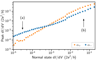
Experimentally, the regimes of dominant single-electron and dominant Andreev current can be distinguished by the dependence of the current on the normal-state conductance of the tunnel junctions Ruby et al. (2015). While the single-electron current is proportional to the normal-state conductance, the Andreev current has a sublinear dependence as a result of the tunneling rates appearing in the denominator of the bound-state resonance. The two regimes are also characterized by different asymmetries between the peak heights of the positive- and negative-voltage resonant Andreev peaks at . Analyzing the peak conductances at positive and negative bias Ruby et al. (2015), one finds that in the regime of dominant single-electron tunneling, their ratio is equal to . This uses the fact that the broadening is dominated by the relaxation rates and . In the regime of dominant resonant Andreev processes, the broadening is dominated by the tunneling rates , leading to an inversion of the ratio of peak heights which is now equal to .
S2.3.2 Photon-assisted resonant Andreev reflections through YSR states
It is natural to expect that HF radiation modifies the tunneling rates for electrons and holes due to photon emission and absorption processes. As the rates describe tunneling of single electrons and holes, we assume that the corresponding sideband spacing is equal to and that the weights of the sidebands are again given in terms of Bessel functions. We thus make the replacements
| (S31) | ||||
| (S32) | ||||
| (S33) |
in Eqs. (S25) and (S26), where we defined . The corresponding definitions for replace and . In this form, the rates account for the electron and hole tunneling rates and resulting broadening, including absorption and emission of any number of photons. Our theoretical simulations of photon-assisted tunneling into YSR states are based on these expressions combined with the current equations (S25) and (S26). We note that it is possible to give a systematic derivation of these expressions for photon-assisted tunneling through YSR states in the framework of a Keldysh Green function approach. This is beyond the scope of the present paper and will be presented in a separate publication.
S3 Further comparison of experiment and theory
S3.1 Simulations of photon-assisted tunneling into pristine substrates
We first consider photon-assisted tunneling into a pristine substrate. Eqs. (S13), (S18), and (S20) give Tien-Gordon-like expressions for the tunneling current, expressing the current in the presence of HF radiation in terms of the current without irradiation. Using these expressions, we can simulate the data in the presence of the HF irradiation based on our data without irradiation. The only free parameter is the damping determining the effective HF voltage at the junction.
Figure S3 shows that corresponding simulations of photon-assisted tunneling are in excellent agreement with our data for all three relevant processes, namely the Josephson peak in Fig. S3a,b [Eq. (S20)], Andreev reflection in Fig. S3c,d [Eq. (S18)], and the coherence peaks in Fig. S3e,h [Eq. (S13)]. In all cases, one correctly reproduces the -like splitting of the peaks as well as the dependence of the sidebands on bias voltage and HF amplitude.
We note that in the experiment, we artificially increased the damping of the transmission line with a attenuator. We observe that the total attenuation slowly fluctuates between . We attribute these fluctuations to external influences such as the He level of the cryostat. For the duration of one measurement sweep, however, we find the attenuation to be constant to a good approximation. We determine the damping by fitting one of the spectra of each sweep using the appropriate Tien-Gordon-like expressions in Eqs. (S13), (S18), and (S20).
S3.2 Basic tunneling processes in the presence of YSR states
S3.2.1 Tunneling processes without HF radiation
We now turn to our data on tunneling in the presence of YSR states. The dd traces in the absence of HF radiation in Figure S4 give an overview of the observed basic tunneling processes. Panel (a) corresponds to a low junction conductance (large tip-sample distance). We observe three peaks at labeled by , which we associate with three YSR states at energies induced by the Mn adatom. At small junction conductance, tunneling into the YSR states at is dominated by single-electron tunneling with rate , followed by inelastic excitation with rate into the quasiparticle continuum of the substrate (see Fig. S5a for a sketch). Similarly, at , tunneling proceeds by a corresponding hole process in which a hole tunnels from the tip into the negative-energy substrate YSR state, followed by a relaxation process with rate which refills the negative energy YSR state Ruby et al. (2015).
For small junction conductances, there are additional resonances at labeled by Ruby et al. (2015). These resonances are weaker compared to the resonances at since they involve thermally excited quasiparticles. For electron tunneling, the process requires thermal occupation of the positive-energy YSR state with rate , before tunneling into the tip with rate (see Fig. S5b for a sketch). This leads to a thermal replica of the YSR state at . The corresponding hole process is found at .
The single-electron tunneling processes are described theoretically by the expression given in Eq. (S25).
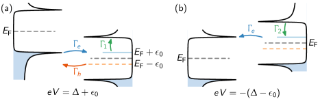
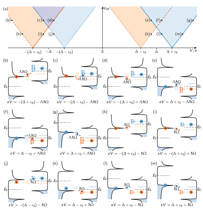
Figure S4b shows data for a high-conductance junction (small tip-substrate distance), so that tunneling into the YSR states is dominated by two-electron tunneling via resonant Andreev reflections (see Fig. S5a for a sketch and discussion above). This tunneling process can be distinguished from single-electron tunneling on the basis of the dependence on the normal-state junction conductance as explained above (see further discussion in Sec. S3.3 below). Resonant Andreev reflection is described theoretically by the expression given in Eq. (S26).
At high junction conductance, we observe additional peaks within the tip gap. The peak at zero bias originates from Josephson tunneling. Multiple Andreev reflections (MAR) through the Pb–Pb junction can be found at for . One also expects that resonant multiple Andreev reflections involving the YSR state appear at Farinacci et al. (2018). It is difficult to attribute the peaks labeled as MAR to a specific process due to the multitude of possible resonant Andreev processes associated to the three YSR states as well as (multiple) non-resonant MARs. The corresponding photon-assisted sidebands also remain unresolved.
S3.2.2 Tunneling processes in the presence of HF radiation
Resonant Andreev reflections in the presence of HF irradiation involve photon emission and absorption for both electron and hole. Extending the processes shown in Fig. 4 of the main text, we provide a more complete portfolio of processes in Fig. S6. These processes demonstrate that there are independent thresholds for electron and hole tunneling, and that these thresholds can be relevant in overlapping regions in the plane, see the overlap regions of the two V shapes centered at and .
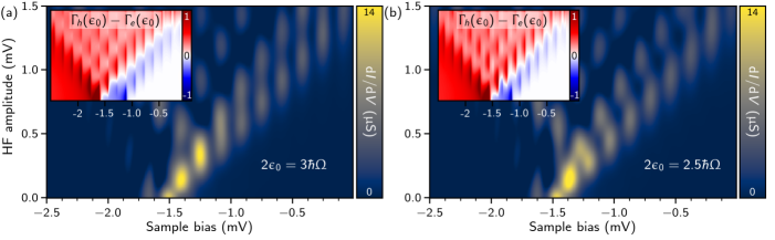
Figure S7 shows theoretical simulations on the double structure at the low-voltage arm of the Y pattern observed at negative biases for high junction conductance. For most parameters, the large asymmetry between hole and electron wave functions of the YSR state implies that only the electron thresholds for photon-assisted tunneling are visible in experiment. The underlying reason is that electron tunneling is weaker due to the smaller electron wavefunction, and thus effectively the rate-limiting process. The only exception occurs at the low-voltage side of the V-shaped region for hole tunneling at negative bias voltages. Here, the rate for electron tunneling, with threshods within the inner V shape, is already large, while hole tunneling is still weak since it is just barely allowed energetically. Thus, one expects to observe additional hole tunneling thresholds in the voltage range, where electron and hole tunneling are of the same order. The insets in Figure S7 show the difference of these tunneling rates. Indeed, the double structure of the low-voltage arm of the Y pattern occurs just in the region where the difference between the tunneling rates becomes small. Panels (a) and (b) differ in the ratio between and . For the parameters of panel (a), electron and hole thresholds appear at the same bias voltage. This is close to the situation in our experiment. In contrast, the two kinds of thresholds are shifted with respect to one another for the parameters in panel (b). Note that the lower structure (associated with hole tunneling) has a smaller apparent slope than the structure just above emerging from electron thresholds. The same apparent difference in slope is also clearly seen in the experimental data included in Fig. 3b of the main text.
S3.3 Simulation parameters
We emphasize that we can simulate the observed spectra for both single-electron and resonant Andreev tunneling via the YSR state based on a few parameters which can be extracted from experiment. This is distinctly different from the simulations in Fig. S3 which use the entire data set in the absence of HF irradiation as input. We now detail how we extract the necessary parameters.
With the exception of the overall tunneling strength at large junction conductance, we extract all parameters from the dd curves for low junction conductance in the absence of HF radiation. We assume that tip and substrate have not only the same gap, but also the same normal state density of states . We can then extract the dimensionless product involving the tunneling amplitude from the expression
| (S34) |
for the normal-state differential conductance of a tunnel junction. This yields . We can now choose parameters such that the peak heights and widths of the dd curves in the absence of HF radiation are well reproduced by Eq. (S25). This can be used to extract from the single-electron tunneling at positive bias voltages and at negative bias voltages. Moreover, the thermal peaks depend sensitively on the relaxation rates and . We also include a Dynes parameter to account for depairing interactions on the superconducting density of states (S15),
| (S35) |
adding an imaginary part to the energy. In addition, we include a Gaussian averaging of the dd traces with width which accounts for instrumental broadening. We find that the following set of parameters reproduces the experimental dd curves:
| (S36) | |||||
| (S37) | |||||
| (S38) | |||||
| (S39) | |||||
| (S40) | |||||
| (S41) |
In particular, we extract the ratio .
With this set of parameters, we can then simulate the dd curves in the presence of the HF radiation, as shown in Fig. 3c of the main paper.
Simulations of photon-assisted tunneling at high junction conductance require only one additional parameter, namely . We choose this parameter so that we find good overall agreement between Eq. (S26) and the measured data for high junction conductance in the absence of the HF radiation. With this procedure, we find . This is within 15% of the value which one would extract from the junction conductance on the basis of Eq. (S34). This completes the parameter set on which the simulation results shown in Fig. 3d of the main text are based.
We note that this parameter set also allows one to corroborate that electron and hole tunneling is slow (fast) compared to the relaxation rates and for low (high) junction conductance, implying that there is a crossover between single-electron and resonant Andreev tunneling. Indeed, we find for the electron and hole tunneling rates, evaluated at the peak of the superconducting density of states (including depairing parameter), the values
| (S42) | |||||
| (S43) |
at low junction conductance, and
| (S44) | |||||
| (S45) |
at large junction conductance. While the first set of tunneling rates are clearly smaller than and , the second are significantly larger.
This can also be double checked as follows. As a result of the asymmetry in the electron and hole wavefunctions, the amplitudes of peak heights for tunneling into the YSR state with reverses as the tip approaches the substrate and the normal state conductance of the junction increases Ruby et al. (2015). This is shown in Fig. S8. In particular, this indicates that panels (a) and (b) of Fig. S4 exhibit data in the regimes of dominant single-electron and dominant Andreev tunneling, respectively (see also the arrows in the figure).
References
- Baumann et al. (2015) S. Baumann, W. Paul, T. Choi, C. P. Lutz, A. Ardavan, and A. J. Heinrich, Science 350, 417 (2015).
- Natterer et al. (2019) F. D. Natterer, F. Patthey, T. Bilgeri, P. R. Forrester, N. Weiss, and H. Brune, Rev. Sci. Instrum. 90, 013706 (2019).
- Friedlein et al. (2019) J. Friedlein, J. Harm, P. Lindner, L. Bargsten, M. Bazarnik, S. Krause, and R. Wiesendanger, Rev. Sci. Instrum. 90, 123705 (2019).
- Seifert et al. (2020) T. S. Seifert, S. Kovarik, C. Nistor, L. Persichetti, S. Stepanow, and P. Gambardella, Phys. Rev. Research 2, 013032 (2020).
- Tien and Gordon (1963) P. K. Tien and J. P. Gordon, Phys. Rev. 129, 647 (1963).
- Tinkham (2004) M. Tinkham, Introduction to Superconductivity, 2nd ed. (Dover, 2004).
- Note (1) One can equivalently consider the tunneling process as energy conserving (in the absence of the radiation field) with different chemical potentials of source and drain, or the chemical potentials as identical, but the tunneling process as changing the electron energy by . We base pictorial representations of the tunneling processes on the first possibility. The second possibility is adapted to the time-dependent tunneling Hamiltonian (S8), and we use corresponding language here when discussing the theoretical calculations.
- Zimmermann and Keck (1996) U. Zimmermann and K. Keck, Z. Phys. B 101, 555 (1996).
- Ingold and Nazarov (1992) G.-L. Ingold and Y. V. Nazarov, in Single Charge Tunneling, NATO ASI Series B, edited by H. Grabert and M. H. Devoret (Plenum Press, New York, 1992) Chap. 294, pp. 21–107.
- Note (2) The Josephson peak can also be described within the RCSJ model, expressing the Josephson current in terms of the phase difference across the junction and computing the (Langevin) dynamics of the phase to linear order in the Josephson energy. While one obtains the same result, this calculation requires one to include only classical voltage fluctuations.
- Falci et al. (1991) G. Falci, V. Bubanja, and G. Schön, Z. Phys. B 85, 451 (1991).
- Ivanchenko and Zil’berman (1968) M. Ivanchenko and L. A. Zil’berman, Zh. Eksp. Teor. Fiz. 55 (1968), [Sov. Phys. JETP 28, 1272 (1969)].
- Grabert and Ingold (1999) H. Grabert and G.-L. Ingold, Superlatt. Microstruct. 25, 915 (1999).
- Naaman et al. (2001) O. Naaman, W. Teizer, and R. C. Dynes, Phys. Rev. Lett. 87, 097004 (2001).
- Ruby et al. (2015) M. Ruby, F. Pientka, Y. Peng, F. von Oppen, B. W. Heinrich, and K. J. Franke, Phys. Rev. Lett. 115, 087001 (2015).
- Farinacci et al. (2018) L. Farinacci, G. Ahmadi, G. Reecht, M. Ruby, N. Bogdanoff, O. Peters, B. W. Heinrich, F. von Oppen, and K. J. Franke, Phys. Rev. Lett. 121, 196803 (2018).