Pulse percolation conduction and multi-value memory
Abstract
We develop a theory of pulse conduction in percolation type of materials such as noncrystalline semiconductors and nano-metal compounds. For short voltage pulses, the corresponding electric currents are inversely proportional to the pulse length and exhibit significant nonohmicity due to strong local fields in resistive regions of the percolation bonds. These fields can trigger local switching events incrementally changing bond resistances in response to pulse trains. Our prediction opens a venue to a class of multi-value nonvolatile memory implementable with a variety of materials.
I Introduction
Nonvolatile memory cells are often based on disordered materials, noncrystalline or compound, with percolation conduction. Percolation in these systems efros ; shik ; snarskii is due to exponentially strong variations in local resistivities and the macroscopic conductivity is dominated by the bonds of the corresponding smallest random resistors allowing electric connectivity. Relevant for memory applications are percolation materials exhibiting plasticity, i. e. the ability to change their resistances in response to electric bias. They include metal oxides and chalcogenide compounds used respectively with resistive random access memory (RRAM) lanza2014 and phase change memory (PCM), sebastian2019 granular metals, gladskikh2014 and nano-composites.song2016
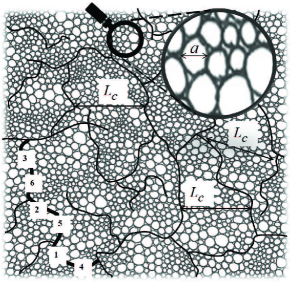
As a quick reminder, Fig. 1 shows random resistors forming bonds in a percolation cluster of correlation radius (mesh size) . The standard treatment assumes time independent currents continuous through the bonds. Because the bond constituting microscopic resistors are exponentially different, the current continuity requires significantly different local electric fields through them. The highest of those local fields produces the exponentially strong nonohmicity of percolation materials. shklovskii1976 ; shklovskii1979 ; aladashvili1989 ; patmiou2019
One distinct feature introduced here is that local electric fields in percolation bonds can be strong enough to structurally modify the underlying material through nonvolatile changes in its local resistivities; hence, percolation with plasticity (PWP).
Another feature introduced here to percolation analyses is the nonstationary pulse-shaped electric bias characteristic of nonvolatile memory operations. We will describe its related current-voltage characteristics and local switchings with fractional changes in the macroscopic resistance due to individual pulses. That feature appears similar to that of the spike-timing-dependent-plasticity (STDP) central to the functionality of neural networks (see fiete2010 ; markram2011 and references therein). From the practical standpoint, it paves a way to PWP multi-valued memory operated in the pulse regime and implementable with a variety of materials.
II Standard percolation vs. PWP
We start our discussion by outlining the concept of standard percolation juxtaposed with that of PWP.
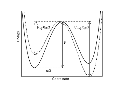
1) Standard percolation efros ; shik ; snarskii is dominated by the sparse, infinite, and conducting cluster between two large electrodes. That cluster’s bonds consist of minimally strong resistors with total concentration sufficient to form a connected structure. It is effectively uniform over distances (Fig. 1). Each bond consists of a large number () of random resistors, where quantities are more or less uniformly distributed in the interval . The physical meaning of depends on the type of system. For definiteness, we assume here corresponding to random barriers in noncrystalline materials illustrated in Fig. 3, where is the Boltzmann’s constant and is the temperature. In reality, the nature of percolation conduction can be more complex including e. g. finite size effects and thermally assisted tunneling between microscopic resistors in nanocomposites. lin2013 ; eletskii2015 These complications will not qualitatively change our conclusions.
As illustrated in Fig. 3, the bond forming microscopic resistors exhibit non-ohmicity shklovskii1979 ; patmiou2019 due to the field induced suppression of their barriers . A symmetric barrier of width is suppressed by , where and are the field strength on and voltage drop across -th resistor, and is the electron charge. The transition rates along and against the field are proportional to yielding the multiplier in the equation for current,
| (1) |
Because of the continuity of electric current and resistors’ nonohmicity, the applied voltage concentrates on the strongest resistor of a percolation bond (resistor 1 in Fig. 1) suppressing it to the level of the next strongest (resistor 2 in Fig. 1), so the two equally dominate the entire bond voltage drop. It then suppresses the next-next strongest resistors, etc. As a result, the percolation cluster changes its structure, resulting in the macroscopic non-ohmic conductivity.shklovskii1979 ; patmiou2019 ; shklovskii1976 ; aladashvili1989
Note the above outlined concept of fields concentrating on most resistive elements implies significant microscopic recharging necessary to create such strong fields. The recharging occurs over the relaxation times , where ps depending on the type of system. Here corresponds to the random barriers depicted in Fig. 3 and varies between different microscopic regions; they are exponentially higher for most resistive regions. The microscopic recharging while tacitly implied in the original non-ohmicity work, shklovskii1979 ; patmiou2019 ; shklovskii1976 ; aladashvili1989 was insignificant there due to the imposed steady state conditions, i. e. long enough time .
Three assumptions underly the standard percolation theory: (a) The topology of infinite percolation cluster between two electrodes. (b)The volatility of bias induced changes: local resistances adiabatically following voltages . (c) The quasistatic nature of biasing steady over times exceeding the local relaxation times .
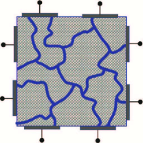
2) PWP systems violate all three of the above assumptions by: (a) opening a possibility of multiple () electrodes patmiou2019 as signal entrances/ports and not assuming the system dimensions exceeding and requiring description beyond the standard percolation theory raikh ; patmiou2019 ; (b) allowing for bias induced nonvolatile changes; and (c) operating under pulse shaped bias typical of neural networks (STDP). (The term “percolation” in PWP still reflects the underlying transport topology.)
We address these differences as follows. (a) Keeping in mind the case of multiple electrodes and/or below system dimensions, we concentrate on the pulse non-ohmic conduction of a single percolation bond. The case of infinite cluster will be addressed in passing [see Eq. (8)]. (b) We will explicitly incorporate the possibility of nonvolatile changes. (c) We develop a theory of non-ohmic percolation in the pulse regime.
III Non-ohmic pulse percolation
Consider the non-ohmic conductivity of a series of random resistors, with in in response to a voltage pulse of length [task (c) above]. A key addition to the standard dc analysis shklovskii1976 is the separation of all resistors into two groups: ‘slow’ () and ‘fast’ (). ‘Fast’ resistors maintain the current continuity adjusting their currents to local voltages as described in Eq. (1). However, ‘slow’ resistors lag behind thus operating as capacitors (for short enough recharging processes) and not developing any significant voltage drops across them.
The concept of slow resistors acting in a manner of capacitors has been proposed and verified earlier. dyre2000 ; abje2016 It may be appropriate to additionally explain here that capacitors do not accommodate significant voltages when in series with resistors because the former conduct due to displacement currents, , while the latter currents are real, where is the electric field strength, is the dielectric permittivity, and is the conductivity. The same current through capacitors is due to the rate of field change, unrelated to voltage, rather than the field itself proportional to voltage in resistors. Relating this understanding with microscopic models, we note that the displacement currents are due to charging/discharging processes in, say, capacitor electrodes, or in potential wells in Fig. 3, or in certain defect configurations responsible for electric potential distributions in percolation clusters.
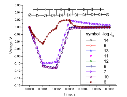
The resistor/capacitor equivalent circuit interpretation opens a pathway to equivalent circuit modeling. Furthermore, because the current-voltage characteristics of Eq. (1) are similar to that of a diode, the nonohmic resistors can be represented by diodes thus allowing the standard PSPICE circuit modeling. Some results of such modeling are presented in Fig. 4.
We conclude that the applied voltage is distributed mostly among the fast resistors. For that group, the voltage distribution is the same as for the dc voltage case, shklovskii1976
| (2) |
Here corresponds to the smallest value resistor affected by the bias and is voltage across the bond of length .
Presenting the total current in the form,
| (3) |
the condition of current continuity becomes,
| (4) |
Substituting the latter into Eq. (2) and replacing the sum with integral, yields,
| (5) | |||||
where is the total number of resistors in the bond. The multiplier in the integrand of Eq. (5) is the probability density normalized to resistors per bond. Note that gives the average difference between two successive values of ’s with being the number of resistors per bond of the percolation cluster. Its numerical value is estimated as shklovskii1976 ; raikh ; levin1987 .
Expressing
| (6) |
and considering Eq. (3) yields,
| (7) |
This result applies when the pulse time is shorter than the maximum relaxation time and is formally different from that of dc analysis shklovskii1976 by the substitution in Eq. (5). The two results coincide when . The dependence reflects the fact that the number of contributing ‘fast’ resistors decreases along with . We note that the scaling is close to the results of numerical modeling schroder2008 for ac percolation current when we set .
While we do not systematically consider the pulse conduction of the entire percolation cluster, it can be advanced based on the published approaches shklovskii1979 ; patmiou2019 with the above proposed modification, . This predicts the following current voltage characteristics,
| (8) |
Note that Eq. (8) functionally presents the well known Poole-Frenkel law for nonohmic conduction, however its exponent is now dependent on the voltage pulse duration, which remains to be addressed experimentally.
IV Pulse induced switching in PWP
It follows from Eqs. (4) and (6) that the highest voltage drop is on the largest-valued resistor (1 in Fig. 1),
| (9) |
which can be a significant fraction of the total applied voltage. The next high and other subsequent voltages (on resistors 2, 3, etc.) are incrementally smaller, , .

Numerically, increment can be quite appreciable, V, corresponding to rather high operational temperatures K of solid state memory cells. niraula2017 Such exceeds the observed statistical dispersion of threshold voltages karpov2008 that is below 0.05 V. Therefore, local voltages differ from each other enough to provide distinct switching events following the hierarchy of local resistors.
With the latter observation in mind, one can describe the pulse driven evolution of a PWP bond. Each microscopic bond element can exist in either high- or low-resistive state whose resistances, namely and , are orders of magnitude different. Because of the inherent randomness, values of form a broad spectrum, each being well above . Before pulse application, all the elements are in their high resistive state having random resistances . The applied bias concentrated on the strongest resistor (in the manner of Fig. 1) will change it from to by switching, i. e. by long lived structural transformation not responsive to subsequent voltage variations. That process takes time equal to pulse length, since the highest affected resistor is defined by the condition that it accommodates voltage during that time. The end of the process coincides with the end of pulse, after which the system finds itself under no bias, with resistance decreased by a factor . The next pulse will similarly eliminate the second strong resistor decreasing the integral bond resistance by another factor , etc. as illustrated in Fig. 5.
Note that the resistance graph in Fig. 5 presents the average picture: in reality, the spectrum of is not equidistant leading to variations between the step changes in . Secondly, we have tacitly assumed instantaneous switching events. In reality, the switching time (between the field application and structural transformation) depends on the field strength and becomes sufficiently short (in sub-nanoseconds) for rather strong fields. karpov2008 ; karpov2008a ; krebs2009 ; bernard2010 ; sharma2015 ; you2017
Empirically, the fields reliably leading to switching are in the range of MV/cm. The following estimate will show that such strong local electric fields are achievable. Assuming nm and yields nm. The strongest field in the bond is estimated by our theory as , and since , one gets V. The latter corresponds to a fairly attainable electric potential drop of kV across cm thick samples.
V Multi-valued memory
The sequences of stepwise resistance changes can be used as multiple memory records in PWP materials. The number of different memory values (steps) is estimated as , i. e.,
| (10) |
For a rough numerical estimate, we use as before , and , which yields . That number can be further increased by tweaking and . Combining the latter with large numbers of PWP pathways ( in Fig. 2) promises memory density above the current technology.
Presently, we are aware of only indirect evidence of sequential changes in resistance by pulses or continuous voltage ramping. song2016 ; gladskikh2014 ; wright2011 We hope that our predictions can trigger additional experiments that are helpful for determining the range of voltages which can cause sequential modifications (switching), the corresponding current-voltage characteristics that depend on pulse duration, and the number of switching events.
Two comments are in order here. The first one is related to the record erasing mechanisms. A possible answer refers to the known mechanisms of PCM and RRAM reset processes by Joule heat anneal and/or by using bipolar switching. For example, a moderate electric current during long enough time can anneal the pulse switched conducting regions to their original dielectric state. Alternatively, using materials with a degree of ferroelectricity can utilize the opposite polarity pulses for reverse switching. karpov2017
Secondly, our analysis of transport in a bond of random diodes might call upon building artificially assembled series of purposely different diodes. While they may be more controllable than the natural noncrystalline materials, their cost and dimensions remain questionable.
VI Conclusion
In conclusion, we have developed a theory of pulse non-ohmic transport in macro-bonds of percolation clusters. Our analysis predicts pulse train triggered multiple switching events in microscopic regions of PWP macro-bonds incrementally changing the logarithms of their resistances. These changes can pave a way to a class of superior multi-valued memory implementable with a variety of materials. The above analysis outlines the range of electric fields and material parameters suitable for PWP multivalued memory. Various experimental verifications are called upon including pulse regime nonohmicity and switching in percolation systems and properties of percolation clusters with multiple electrodes.
References
- (1) B. I. Shklovskii, A. L. Efros, Electronic Properties of Doped Semiconductors, Springer, 1984.
- (2) A. Y. Shik, Electronic properties of inhomogenious semiconductors, Gordon and Breach (1995).
- (3) A. A. Snarskii, I. V. Bezsudnov, V. A. Sevryukov, A. Morozovskiy, J. Malinsky, Transport Processes in Macroscopically Disordered Media: From Mean Field Theory to Percolation, Springer, NY 2016).
- (4) M. Lanza, A Review on Resistive Switching in High-k Dielectrics: A Nanoscale Point of View Using Conductive Atomic Force Microscope, Materials 7, 2155-2182 (2014); doi:10.3390/ma7032155
- (5) A. Sebastian, M. Le Gallo and E. Eleftheriou, Computational phase-change memory: Beyond von Neumann computing, J. Phys. D: Appl. Phys. 52, 44 (2019).
- (6) I. A. Gladskikh, N. B. Leonov, S. G. Przhibel’skii, and T. A. Vartanyan, The optical and electrical properties and resistance switching of granular films of silver on sapphire, J. Opt. Technol. 81 280 (2014).
- (7) Y. Song, H. Jeong, S. Chung, G. H. Ahn, T-Y Kim, J. Jang, D. Yoo, H. Jeong, A. Javey, T. Lee, Origin of multi-level switching and telegraphic noise in organic nanocomposite memory devices, Scientific Reports, 6, 3967 (2016); DOI: 10.1038/srep33967.
- (8) B. I. Shklovskii, Nonohmic hopping conduction, Soviet Physics: Semiconductors, 10, 855 (1976) [Fiz. Tekh. Poluprovodn. 10, 1440 (1976)]
- (9) B. I. Shklovskii, Percolation mechanism of electrical conduction in strong electric fields, Soviet Physics: Semiconductors, 13, 53 (1979) [Fiz. Tekh. Poluprovodn. 13, 93 (1979)]
- (10) D.I. Aladashvili, Z.A. Adamiya, K.G. Lavdovskii, E.I. Levin, and B.I.Shklovskii, Poole-Frenkel effect in the hopping conduction range of weakly compensated semiconductors, Fiz. Tekh. Poluprovodn, 23, 213 (1989) [Sov. Phys. Semicond. 23, 132 (1989)
- (11) Maria Patmiou, D. Niraula, and V. G. Karpov, The Poole-Frenkel laws and a pathway to multi-valued memory, Appl. Phys. Lett. 115, 083507 (2019); https://doi.org/10.1063/1.5115991.
- (12) I. R. Fiete, W. Senn, C. Z.H. Wang, and R.H.R. Hahnloser, Spike-Time-Dependent Plasticity and Heterosynaptic Competition Organize Networks to Produce Long Scale-Free Sequences of Neural Activity, Neuron, 65, 563–576 (2010).
- (13) H. Markram, Wulfram Gerstner, P. J. Sjöström, A history of spike-timing-dependent plasticity, Frontiers in Synaptic Neuroscience, 3, Article 4 (2011); doi: 10.3389/fnsyn.2011.00004.
- (14) K-C Lin, D. Lee, L. An, Y. H. Joo, Finite-Size Scaling Features of Electric Conductivity Percolation in Nanocomposites, Nanoscience and Nanoengineering 1, 15 (2013); DOI: 10.13189/nn.2013.010103
- (15) A. V. Eletskii, A. A. Knizhnik, B. V. Potapkin, J. M. Kenny, Electrical characteristics of carbon nanotube-doped composites, Uspekhi Fizicheskikh Nauk 185, 225 (2015) [Physics - Uspekhi 58 209 (2015)]; doi: https://doi.org/10.3367/UFNe.0185.201503a.0225
- (16) J. C. Dyre and T. B. Schrøder, Universality of ac conduction in disordered solids, Reviews of Modern Physics, 72, 873 (2000).
- (17) S. M. Abie, J. Bergli, Y. Galperin and 0. Grottem Martinsen, Universality of AC conductance in human hair, Biomed. Phys. Eng. Express 2 027002 (2016).
- (18) T. B. Schroder and J. C. Dyre, ac Hopping Conduction at Extreme Disorder Takes Place on the Percolating Cluster, Phys. Rev Lett. 101, 025901 (2008).
- (19) M. E. Raikh and I. M. Ruzin, Transmittancy fluctuations in randomly non-uniform barriers and incoherent mesoscopic in Mesoscopic Phenomena in Solids, edited by B. L. Altshuller, P. A. Lee, and R. A. Webb, (Elsevier, NY, 1991), p. 315.
- (20) E. I. Levin, I. M. Ruzin, B. I. Shklovskii,Transverse hopping conduxtivity of amorphous films in strong electric fields, Soviet Physics: Semiconductors, 22, 401 (1987) [Fiz. Tekh. Poluprovodn. 22, 642 (1987)]
- (21) D. Niraula and V. G. Karpov, Heat Transfer in Filamentary RRAM Devices, IEEE Transactions on Electron Devices, 64, 4106 (2017),
- (22) I. V. Karpov, M. Mitra, D. Kau, G. Spadini, Y. A. Kryukov, and V. G. Karpov, Evidence of field induced nucleation in phase change memory, Appl. Phys. Lett., 92, 173501 (2008).
- (23) V. G. Karpov,Y. A. Kryukov, I. V. Karpov and M. Mitra, Field-induced nucleation in phase change memory, Phys. Rev. B, 78, 052201 (2008).
- (24) D. Krebs, S. Raoux, C. T. Rettner, G. W. Burr, M. Salinga, M. Wuttig, Threshold field of phase change memory materials measured using phase change bridge devices. Appl. Phys. Lett. 95,082101, (2009); https://doi.org/10.1063/1.3210792.
- (25) Y. Bernard, P. Gonon, and V. Jousseaume, V. Resistance switching of Cu/SiO2Cu/SiO2 memory cells studied under voltage and current driven modes. Appl. Phys. Lett. 96, 193502, https://doi.org/10.1063/1.3428779 (2010).
- (26) A. A. Sharma, I. V. Karpov, R. Kotlyar, J. Kwon, M. Skowronski, and J. A. Bain Dynamics of electroforming in binary metal oxide-based resistive switching memory. J. Appl. Phys. 118, 114903,(2015); https://doi.org/10.1063/1.4930051.
- (27) J. Yoo, J.Park, J. Song, S. Lim, H. Hwang, Field-induced nucleation in threshold switching characteristics of electrochemical metallization devices. Appl. Phys. Lett. 111, 063109, (2017); https://doi.org/10.1063/1.4985165.
- (28) C. D. Wright, Y. Liu , K. I. Kohary , M. M. Aziz, and R. J. Hicken, Arithmetic and biologically-inspired computing using phase-change materials, Adv. Mater. 23 3408, (2011).
- (29) V. G. Karpov, D. Niraula, I. V. Karpov, and R. Kotlyar, Thermodynamics of Phase Transitions and Bipolar Filamentary Switching in Resistive Random-Access Memory, Phys. Rev. Applied, 8, 024028 (2017).