Polar InGaN/GaN quantum wells: Revisiting the impact of carrier localization on the green gap problem
Abstract
We present a detailed theoretical analysis of the electronic and optical properties of -plane InGaN/GaN quantum well structures with In contents ranging from 5% to 25%. Special attention is paid to the relevance of alloy induced carrier localization effects to the green gap problem. Studying the localization length and electron-hole overlaps at low and elevated temperatures, we find alloy-induced localization effects are crucial for the accurate description of InGaN quantum wells across the range of In content studied. However, our calculations show very little change in the localization effects when moving from the blue to the green spectral regime; i.e. when the internal quantum efficiency and wall plug efficiencies reduce sharply, for instance, the in-plane carrier separation due to alloy induced localization effects change weakly. We conclude that other effects, such as increased defect densities, are more likely to be the main reason for the green gap problem. This conclusion is further supported by our finding that the electron localization length is large, when compared to that of the holes, and changes little in the In composition range of interest for the green gap problem. Thus electrons may become increasingly susceptible to an increased (point) defect density in green emitters and as a consequence the nonradiative recombination rate may increase.
I Introduction
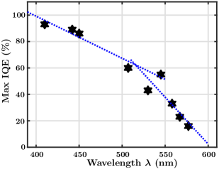
Wurtzite InGaN/GaN quantum well (QW) systems, grown along the polar -axis, have allowed the realization of optoelectronic devices that emit bright light over a wide spectral range, including emission at previously unattainable short wavelengths, with unprecedented efficiency. Ponce and Bour (1997); Akasaki and Amano (2006); Nakamura et al. (1993) However, the internal quantum efficiency (IQE) drops rapidly for emission wavelengths beyond the blue spectral range, Mukai et al. (1999); Humphreys (2008) as shown in Fig. 1. This effect is known as the “green gap” problem. Humphreys (2008); Krames et al. (2007) Given the dramatic reductions in energy use, and the associated reduction in carbon emissions which would result from the development of all-LED white light sources, utilizing red, green, and blue LEDs, Humphreys (2008) the understanding and circumvention of the green gap problem represents an urgent scientific and ecological objective. However, the origin of this phenomenon in InGaN-based emitters is still a matter of some debate. Focusing on -plane InGaN/GaN QWs, the green gap problem has been discussed on the basis of mainly three factors and their combined effect on the radiative/nonradiative recombination processes in these heterostructures.
The first of these factors is the decreasing material quality of InGaN/GaN QW systems with increasing In content. Crawford (2009); Langer et al. (2013a); Armstrong et al. (2012); Massabuau et al. (2014); Uedono et al. (2014); Hammersley et al. (2015) To grow InGaN QWs emitting in the green spectral region, low growth temperatures are typically required to suppress In atom desorption during growth and thus to achieve higher In contents. Hammersley et al. (2015) The results by Hammersley et al. Hammersley et al. (2015) indicated that these low growth temperatures lead to increased (point) defect densities. Additionally, with increasing In content in the well, the lattice mismatch between the InGaN QW and the GaN barrier increases, which encourages stress relaxation through defect formation. Crawford (2009); Langer et al. (2013a); Massabuau et al. (2014) In general, defects and structural imperfections can serve to reduce the IQE by acting as nonradiative recombination centers. Langer et al. (2013a, 2011) Some of these issues may be reduced using innovative growth techniques. Armstrong et al. (2015a); Zhu et al. (2017); Tian et al. (2017)
The second factor contributing to the green gap problem is a property intrinsic to wurtzite -plane InGaN/GaN QWs and is also related to the increase in lattice-mismatch induced strain with increasing In content. The increase in strain leads to an increase in the piezoelectric polarization vector field inside the InGaN QW. Ambacher et al. (2002); Patra and Schulz (2017) The resultant intrinsic electrostatic built-in field leads to a separation of electron and hole wave functions along the growth direction. This effect is also known as the quantum confined Stark effect (QCSE). Andreev and O’Reilly (2001) Thus, the higher the In content the larger the built-in field and the greater the reduction in the radiative recombination rate due to the separation of charge carriers.
Taken together, factor one (increased defect densities and nonradiative recombination rates), and factor two (reduction in radiative recombination rate) will have a negative impact on the radiative optical properties of InGaN-based light emitters. As discussed above, these limitations will be worsened for higher In contents and thus emission in the green spectral region.
Very recently, a third factor contributing to the green gap problem has received significant attention: carrier localization Yang et al. (2014); Auf der Maur et al. (2016); Jones et al. (2017); Karpov (2017, 2018); Nippert et al. (2016) due to (random) alloy fluctuations as well as structural inhomogeneities. Different groups have concluded that the alloy related carrier localization effects lead to an in-plane separation of electrons and holes in addition to the built-in field induced effect, described above. Auf der Maur et al. (2016); Karpov (2017, 2018); Watson-Parris et al. (2011)
Despite the large quantity of recent studies on this topic, there remains a significant degree of uncertainty as to which contribution is the dominant factor for the green gap problem, and accordingly how it may be best circumvented. Many works impute the green gap primarily to an increased defect density. Langer et al. (2011, 2013a); David et al. (2019) Other studies focus on carrier localization effects as the main source of this effect, Nippert et al. (2016); Auf Der Maur and Yu Karpov (2017); Karpov (2018) and assume that non-radiative recombination effects (such as defect-related Schockley-Read-Hall recombination) are independent of the In content. These recent theoretical studies, whereby the green gap is attributed to material intrinsic carrier localization result in a very pessimistic outlook in which the green gap cannot be closed via technological optimization of InGaN QWs. Auf Der Maur and Yu Karpov (2017); Karpov (2018) This emphasis on localization as a negative feature of InGaN QWs is an interesting development, given that localization is widely regarded as the mechanism by which InGaN-based light emitting devices, with their high defect densities, exhibit high efficiencies at all. Chichibu et al. (2006); Dawson et al. (2016)
Given this ambiguity and disagreement in the literature, and the distinct approaches that each of these hypotheses suggest for further development of InGaN technologies, we revisit in this work the contentious issue of the origin of the green gap. Our results show that the localization characteristics in InGaN QWs do not change strongly from blue to green emitters, but rather change very little in this wavelength range. This lack of variation in localization effects has not been considered or discussed in works attributing the green gap problem to carrier localization; only absolute numbers are discussed rather than focussing on changes in the carrier localization effects. Given that blue LEDs are very efficient, and that alloy induced carrier localization effects do not change dramatically between blue and green emitters, only slight changes to the radiative recombination rate would be expected. This casts doubt on the assumption that the nonradiative recombination due to defects is constant and In content independent; if it were, the sharp drop in max IQE (see Fig. 1) and/or wall plug efficiency (WPE), as we will discuss below, would be difficult to explain. So contrary to the pessimistic conclusion that due to alloy induced carrier localization effects the green gap problem cannot be solved, innovative growth techniques may allow for its closure. For example, Haller et al. Haller et al. (2017) have recently suggested that by growing an InGaN underlayer prior to the QW layers, it is possible to getter nonradiative point defects to the underlayer, thereby increasing efficiency.
In this work we come to our conclusion by using an atomistic multi-band tight-binding (TB) model that we first rigourously benchmark against experimental data for InGaN/GaN QWs emitting over a wide range of emission wavelengths. We study the photoluminescence (PL) peak energies, widths, and carrier localization lengths. Overall very good agreement between theory and experiment is found. This highlights that carrier localization effects are accurately described by our model, thus providing a solid foundation for analyzing and predicting the importance of carrier localization for the green gap problem.
The manuscript is organized as follows. In Sec. II.1 we introduce the theoretical framework. In Sec. II.2 structural properties of QW structures for the different In contents will be discussed along with a description how these are treated in the modeling. The results of our calculations are presented in Sec. III. A theory experiment comparison is given in Sec. III.2. The analysis of the carrier localization length is presented in Sec. III.3, followed by investigating the electron-hole wave function overlap as a function of In content in Sec. III.4. Our work is summarized in Sec. IV. Further details of the calculations and further supporting results are given in an Appendix.
| Quantity | Experiment | Theory EMA | Theory TBM | |||||||||||
|---|---|---|---|---|---|---|---|---|---|---|---|---|---|---|
| Indium content (%) | 53 | 123 | 153 | 192 | 252 | 5 | 12 | 15 | 19 | 25 | 5 | 10 | 15 | 25 |
| Well width (nm) | 2.50.3 | 2.70.3 | 2.90.3 | 3.20.2 | 3.30.2 | 2.5 | 2.7 | 2.9 | 3.2 | 3.3 | 2.85 | 2.9 | 3 | 3.5 |
| PL peak energy (eV) | 3.32 | 2.99 | 2.71 | 2.36 | 2.16 | 3.27 | 2.88 | 2.69 | 2.49 | 2.14 | 3.23 | 2.96 | 2.62 | 1.99 |
| FWHM (meV) | 23 | 62 | 76 | 56 | 61 | 34 | 50 | 58 | 69 | 75 | 35 | 59 | 84 | 93 |
II Theory and quantum well system
In this section we briefly review the theoretical framework used and the QW model systems studied. We start in Sec. II.1 with the theoretical framework and briefly introduce its main ingredients. In Sec. II.2 the supercell employed in our calculations is described.
II.1 Theoretical framework
Our theoretical framework is based on an atomistic nearest neighbor TB model. The matrix elements of the TB Hamiltonian describing the binary materials are treated as free parameters, which have been obtained by fitting the TB band structures to hybrid functional density functional theory data. Caro et al. (2013) While for In and Ga atoms the nearest neighbor environment always consists of N atoms, N atoms can have variable numbers of In and Ga atoms as nearest neighbors. To determine the N-onsite energies in an alloy, weighted averages of the InN and GaN binary values have been used, which is a widely used approximation in TB models for alloys. O’Reilly et al. (2002); Li and Pötz (1992); Boykin et al. (2007)
To achieve an atomistic description of the strain field in a strained InGaN QW, we utilize a valence force field (VFF) model. Caro et al. (2013) By minimizing the VFF elastic energy of the simulation supercell, the relaxed atomic positions of the system are determined. These then serve as input for the TB model, which accounts for the effect of strain on the electronic structure by an on-site correction to the matrix elements, the method of which is presented in Ref. Caro et al., 2013.
In addition to (local) strain effects, (local) built-in polarization fields also affect the electronic and ultimately the optical properties of InGaN/GaN QWs. Williams et al. (2005); Schulz et al. (2015a, b) In these systems in particular the strain induced piezoelectric contribution plays a major role. Williams et al. (2005); Patra and Schulz (2017); Andreev and O’Reilly (2001); Patra et al. (2017) Macroscopic, as well as local polarization effects are included in the calculation via the local polarization theory described in Ref. Caro et al., 2013.
By diagonalizing the constructed TB Hamiltonian matrix, the corresponding single-particle states are obtained. In previous work, Schulz et al. (2015a); Tanner et al. (2018); Dawson et al. (2016) we have shown that for -plane InGaN/GaN QWs at low temperatures, especially for well thicknesses exceeding 2.5 nm, Coulomb effects mainly lead to energetic shifts of the peak positions in the optical spectra but do not alter the localization characteristics significantly. Given that we are interested in carrier localization effects and characteristics, neglecting Coulomb (excitonic) effects is a reasonable starting point for our analysis. To study the optical properties of -plane InGaN/GaN QWs with varying In content at low temperatures, we use single-particle states and energies in conjunction with Fermi’s golden rule to obtain PL emission spectra. Schulz et al. (2006, 2015a) For low temperature and low carrier density studies we calculate the dipole matrix elements for electron and hole ground states for each microscopic alloy configuration. Even though a large number of microscopically different configurations have been used (see below), in Fermi’s Golden rule the -function, describing the energy conservation, has been replaced by a Lorentzian function with a standard deviation of 7 meV. For the composition range studied and for the number of considered microscopic configurations, this setting results generally in smooth low temperature PL spectra, with the broadening of the -function having a minimal effect on the width of the calculated spectra.
Finally, the supercell that contains the InGaN/GaN QW system and on which the calculations will be performed, has to be defined. This will be the topic of the next section.
II.2 Quantum well structures and simulation supercell
To study the importance of alloy-induced carrier localization to the green gap problem, we have chosen to model -plane InGaN/GaN QWs with In contents of 5%, 10%, 15%, and 25%, covering the blue to green spectral range. We simulate these QW systems using supercells with periodic boundary conditions that contain 81,920 atoms, corresponding to a system size of approximately nm3. The details of the structures used in our theoretical study are labeled as “TBM” in Table 1.
To compare and benchmark our results against literature, we make use of Refs. Watson-Parris et al., 2011, Graham et al., 2005 and Watson-Parris, 2011, where the optical properties of a series of -plane InGaN/GaN QWs have been studied in theoretical and experimental works. The theoretical results of Ref. Watson-Parris, 2011 were obtained in the framework of a modified 3D single-band effective mass approach, further details of which may be found in Ref. Watson-Parris, 2011. The details of the studied QWs are also presented in Table 1; experimental data from Graham et al. Graham et al. (2005) are entitled “Experiment”, while the results of the modified 3D single band effective mass approximation are labeled “EMA”. Since our focus is on general trends with increasing In content, we do not aim for a direct one-to-one comparison with the structures reported in Ref. Graham et al., 2005. Such a one-to-one theory-experiment comparison would in general be difficult, given that the In fractions and well widths reported in Ref. Graham et al., 2005 have been determined by electron energy-loss spectroscopy (EELS) and high resolution transmission electron microscopy (HRTEM), respectively, which result in large errors for the measured In contents and to a lesser degree for the well widths. For instance, when looking at the system with the lowest In content, grown at C, the well width is nm and the In content 5%. We therefore keep uncertainties in mind when comparing with data from Ref. Graham et al., 2005.
For our atomistic theoretical framework, information on the In atom distribution is also required. In the following we assume a random distribution of In atoms, which is consistent with experimental results, for instance, obtained by careful atom probe tomography studies. Graham et al. (2005); Monemar et al. (2002); O’Neill et al. (2003); Smeeton et al. (2003) We highlight that even the 25% In content sample is not expected to deviate from a random In atom distribution as the atom probe analysis in Ref. Galtrey et al., 2008 shows. Also, the same assumption about the random In atom distribution has been made by Watson-Parris et al. Watson-Parris (2011); Watson-Parris et al. (2011) in the modified 3D continuum-model. Since several studies have revealed that the alloy microstructure significantly impacts the optical properties of -plane InGaN QWs, Watson-Parris et al. (2011); Schulz et al. (2015a); Tanner et al. (2016); Auf der Maur et al. (2016); Piccardo et al. (2017); Jones et al. (2017) we have constructed, for each In content, 175 different configurations with different random In atom distributions. This allows us to obtain reliable statistical averages and to calculate quantities such as full width at half maximum (FWHM) of the PL spectra and thus to compare this data with experiment.
Using Fermi’s golden rule to calculate, as detailed above, the low temperature and low carrier density optical spectra in combination with the 175 different microscopic configurations, we find for all but the 25% In case smooth PL spectra; for the 25% In system, we still observe a slightly “noisy” PL spectrum. By using more configurations, or a wider Lorentzian function for each PL peak resulting from the different microscopic configurations, this “noise” could be mitigated; but, in order to keep the settings consistent across the different In contents, such adjustments have not been made. Thus, the predicted FWHM values for the 25% In well should be regarded as a lower bound for this system. Since we want to study the electronic structure and the optical properties in detail and for different temperatures, we consider for higher temperatures and carrier densities not only ground states of each of the microscopic configurations, but also excited states. Thus, we have calculated for each of the 175 different configurations per In content 20 electron and 40 hole states. With this we are able to account for the fact that carriers will populate excited states at elevated temperatures.
As a last ingredient we introduce structural inhomogeneities in the theoretical description, namely well width fluctuations (WWFs) at the upper interface of the well. Watson-Parris (2011); Watson-Parris et al. (2011); Schulz et al. (2015a) Following the experimental and theoretical work in Refs. Watson-Parris, 2011; Watson-Parris et al., 2011; Schulz et al., 2015a, these WWFs are described by disk-like objects with a diameter of approx. 5 nm and a height of 2 monolayers. It should be stressed that these objects allow now, in a spatially restricted region, the presence of In atoms in the GaN barrier. Given that we treat InGaN as a random alloy, the actual shape and form of these WWFs will vary and change from microscopic configuration to microscopic configuration. It should be noted that this situation is different when, for instance, compared to a continuum-based calculation, where the WWF would be rigid object with constant size and shape.
Effects such as penetration of In atoms into the barrier, beyond the above discussed WWFs, have not been included. Neglecting these effects is based on the following arguments given in the literature. First, it has recently been shown that by a careful choice of the growth conditions this effect can be reduced. Massabuau et al. (2017) While this In penetration effect could be expected to be of relevance for the samples of Ref. Graham et al., 2005, in structures grown more recently this effect is expected to be less pronounced. Moreover, Watson-Parris studied such a diffuse upper QW interface and concluded that this factor has no noticeable impact on carrier localization effects. Watson-Parris (2011) This stems from the fact that the distribution of the In atoms, when penetrating into the barrier, is homogeneous in the QW plane while in the observed WWFs the In content is more noticeably concentrated. Thus, the impact of the WWFs on carrier localization characteristics is much more pronounced than a diffuse upper interface. Finally, for a consistent comparison between the results of our model here and those of the modified 3D single-band effective mass model, Watson-Parris (2011); Watson-Parris et al. (2011) the same basic assumptions about the structural properties have been made. Following Ref. Watson-Parris et al., 2011 and based on the other considerations above, we exclude in our model In atom penetration into the barrier, except for effects introduced by WWFs.
III Results
Having introduced the theoretical framework and the InGaN/GaN QW systems to which it is applied, we present in the following subsections the results of our calculations. In a first step, in Sec. III.1, we give an overview of some general aspects of the electronic structure of -plane InGaN/GaN QWs. Special attention is paid to carrier localization effects. This analysis will support and underpin the findings of the following sections. In Sec. III.2 we use the experimental data extracted from Refs. Graham et al., 2005 and Watson-Parris, 2011 to benchmark our theoretical results across the In content composition range from 5% up to 25% and compare also to literature theory data by Watson-Parris et al. Watson-Parris (2011); Watson-Parris et al. (2011) (see above). In the following section, Sec. III.3, we study localization lengths as a function of the In content and temperature for a fixed carrier density. Our calculated values are compared with experimental literature data from the same study Graham et al. (2005) discussed in Sec. III.2. Finally, in Sec. III.4, the electron hole wave function overlaps are investigated. Attention is directed towards the contribution of the in-plane carrier separation to the reduction in the wave function overlap with increasing In content. Both Secs. III.3 and III.4 will shed light on the connection between carrier localization effects and changes in the optical properties of InGaN/GaN QWs when pushing the emission from the blue wavelength regime to the green and orange part of the spectrum.
III.1 General aspects of the electronic structure of -plane InGaN/GaN quantum wells
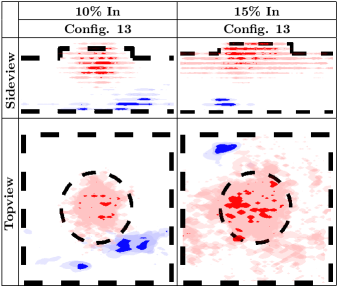
Figure 2 shows isosurface plots of the electron (red) and hole (blue) ground state charge densities for the microscopic configuration (Config.) 13 of InGaN QWs with 10% (left) and 15% In (right). The results are displayed for a sideview, perpendicular to the wurtzite -axis, and a topview, along the wurtzite -axis. Several aspects of these plots are of interest for the results discussed below. First, the side view reveals a salient feature of -plane InGaN QWs: the vertical separation of the electron and hole wave functions due to the built-in field. This significantly reduces the wave function overlap. Second, for both systems we find strongly localized hole ground state wave functions, revealing that random alloy fluctuations are sufficient to give rise to carrier localization effects. This localization of hole states is observed across all configurations. For electrons we find that wave functions are localized by the WWFs. In general, and also as in our previous results, Schulz et al. (2015a); Dawson et al. (2016); Tanner et al. (2018) the hole wave functions are more strongly localized than those of the electrons. We will return to this point later when discussing quantitatively the electron and hole localization lengths.
Taking these two points together, our results show that in polar InGaN/GaN QW systems the interplay between random alloy fluctuations, WWFs, and electrostatic built-in field results in both an out-of plane and an in-plane separation of the carriers. This stems from the fact that holes do not necessarily localize below the WWF where the electron is localized. We note that this in-plane carrier separation is also present in structures without WWFs, as we have discussed in previous studies, that the WWFs enhance, rather than produce, this phenomenon. Tanner et al. (2018) The underling cause of the in-plane separation is that, being separated to opposite ends of the QW by the built-in field, the electrons and hole each inhabit a different alloy/potential landscape, and those regions most energetically favorable for an electron to localize at the upper interface, are mainly uncorrelated with those regions energetically favorable for the holes to localize at the lower interface (cf. Fig. 2). The finding of an in-plane spatial separation is consistent with theoretical work of Watson-Parris et al., Watson-Parris et al. (2011) Auf der Maur et al., Auf der Maur et al. (2016) and Jones et al. Jones et al. (2017) It is also consistent with the pseudo donor-acceptor pair model introduced by Morel et al. Morel et al. (2003) to explain time-resolved optical properties of -plane InGaN/GaN QWs. In Refs. Auf der Maur et al., 2016; Karpov, 2017, 2018 by assuming a constant defect related nonradiative contribution, the in-plane separation or the combination with the built-in field is even regarded as the main driver behind the green gap problem. However, before turning to this question in more detail, we first start with benchmarking our theory against experimental data across the In composition and the resultant emission wavelength range relevant to the green gap problem. We note that our low temperature experimental data indicates (cf. Table 1) that 19% In and a well width of nm is enough to achieve emission in the spectral range relevant to the green gap problem. In the theoretical study of Ref. Auf der Maur et al., 2016, a well width of 3 nm and 30% In was required to push the emission wavelength to a comparable wavelength, bearing in mind that these calculations were carried out for emission at room temperature, the In content in the theoretical study in Ref. Auf der Maur et al., 2016 is noticeably different to the In content in the experimental work in Ref. Graham et al., 2005 (cf. Table 1), while the well width is not vastly different. Therefore, a detailed theory-experiment comparison is important to ensure that the theoretical model describes key optical properties of realistic and experimentally relevant structures correctly before it is applied to analyze the impact of carrier localization on the green gap problem.
III.2 Theory vs. experiment: PL peak position energies and full width at half maximum values
The low temperature and low excitation carrier density optical properties of InGaN/GaN QWs presented in Ref. Graham et al., 2005 provide an ideal starting point for comparing trends predicted by our theory for PL peak energies and FWHM values over a wide In composition range. In Table 1, the optical and structural properties of the studied QW systems are presented and summarized. As already discussed above, our aim is not to match structural properties or PL peak energies exactly. Rather we are interested in studying how the optical properties of polar InGaN/GaN QWs change with increasing In content and if we capture the main features of the measured spectra. When comparing the theoretical and experimental data presented in Table 1, our theory gives a good description of the PL peak energy with increasing In content. Furthermore, we find good agreement with the theoretical data from Refs. Watson-Parris et al., 2011; Watson-Parris, 2011, which used a modified 3D EMA that also accounts for random alloy fluctuations.
In a second step, our calculated FWHM values are compared with both the experimental Graham et al. (2005) and theoretical data Watson-Parris (2011); Watson-Parris et al. (2011) (cf. Table 1). It is important to note that the experimental optical studies have been carried out at low temperatures ( K) and low excitation carrier densities, so that it is reasonable to assume that occupation of excited (electron and hole) states is of secondary importance. Several features of this comparison are now of interest. Looking at Table 1, we observe that over the composition range from 5% to 15% In (PL peak energies between 2.6 eV and 3.35 eV), our theoretical results for the FWHM are in good agreement with the experimental data from Graham et al. Graham et al. (2005) In this energy (wavelength , In content) range an increase in the FWHM with decreasing PL energy (increasing emission wavelength ) is observed. The calculations from Refs. Watson-Parris, 2011; Watson-Parris et al., 2011 in this energy/composition range give always lower numbers, except for the 5% In case. Nevertheless, over the 5% to 15% In content range the trend of increasing FWHM values with decreasing PL peak energy (increasing In content) is also borne out by the EMA. It should be noted that we find good agreement between theory and experiment in terms of FWHM values without introducing In clustering effects, in contrast to a recent study. Di Vito et al. (2019) As already indicated above, even for the higher In content samples, we do not find experimental evidence for clustering. Turning to the higher In content systems (In content %) and lower PL peak energies, eV, both theoretical models predict a further increase of the FWHM. This is in contrast to the experimental data, which reveals a sudden drop in the FWHM in the energy range below eV (samples with 19% and 25% In, cf. Table 1). However, as we have highlighted above, given that these single QW (SQW) systems have been characterized by EELs and HRTEM, both nominal In content and well width may exhibit large error bars. Turning to the literature, recent results on multi QW (MQW) structures at room temperature show that the FWHM increases at longer wavelength/lower PL peak energies. Robin et al. (2018) Obviously, in these MQW systems other factors such as well to well variations could play a role. Thus, future studies, ideally with SQW samples of different In content, could target further careful optical and structural characterization of such systems, to shed more light on our observed discrepancies between theory and experiment. However, such a detailed and refined investigation is beyond the scope of the present study.
Overall, the comparison shows that our theoretical framework gives a good description of several of the optical features of -plane InGaN/GaN QWs across the In content range relevant to the green gap problem. Building on this, we now calculate carrier localization lengths as a function of the In content. This quantity has recently been used to establish a connection between (hole) localization effects and the green gap. Karpov (2017, 2018)
III.3 Carrier localization length
Different approaches have been used in the literature to evaluate the carrier localization length. These include, amongst others: the inverse participation ratio (IPR), Thouless (1974); Wegner (1980); Ludwig et al. (2003) the volume fraction, Chan et al. (2010) and the variance of the position operator. Watson-Parris (2011) Here, we use the IPR to calculate wave function localization lengths. To define the IPR, we recall that the TB wave function can be written as:
| (1) |
The index denotes the orbital type (,,,) in our nearest neighbor TB model and the label runs over the lattice sites of the supercell (). Based on Eq. (1), we can define the IPR as follows: Tanner et al. (2016)
| (2) |
For a Bloch (delocalized) state the IPR would be .Wegner (1980) Conversely, a localized state (only orbital contributions on the same lattice site ) would have an IPR value of . Given that a state with an IPR which is twice that of another state can be regarded two times more localized, we can use the volume of a reference state to associate a given IPR with a length. In this we follow a procedure similar to that of Thouless, Thouless (1974) who defined a localization length of for a cubic lattice with lattice spacing . However, we refine this procedure to account for the fact that we are dealing with a wurtzite crystal structure and more importantly with wurtzite QW systems which exhibit a built-in field. Therefore, we differentiate between the in- and out-of growth plane directions in these systems and go a step further than the isotropic localization length defined in other theoretical studies. Chan et al. (2010); Watson-Parris (2011); Karpov (2017) This treatment allows for a closer comparison between our theory and experimental data that reports on in-plane hole localization lengths. Graham et al. (2005)
To calculate the out-of plane localization length of a given state , we introduce the planar integrated probability density, :
| (3) |
where and are the in-plane (-plane) coordinates and denotes the nth layer along the -axis. This quantity represents a probability density per layer, where gives the probability that the carrier described by state be found in the nth layer of the supercell; , where is the number of -planes in the system. From this one-dimensional probability density we may define an IPR value, and follow Thouless Thouless (1974) to relate this to a length via the formula: , where is the average spacing between -layers in our relaxed supercells.
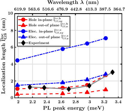
The in-plane localization length can be calculated by building on the out-of plane length and a reference state. We do not go into the detail of the calculations here, but present them in Appendix A. Using this approach we have calculated the in- and out-of plane average ground state (GS) localization lengths for electrons and holes by averaging over the 175 configurations for each In content . The results are shown as a function of the calculated PL peak energies in Fig. 3. The top -axis gives the corresponding emission wavelength . Here and in subsequent localization length plots, electron lengths are given in blue, and holes in red; in-plane lengths are denoted by filled circles, and out-of plane are denoted by filled triangles.
Figure 3 reveals three properties which are general across all quantities. First, the hole ground state wave functions are more localized than those of the electrons, in both the in- and out-of plane dimensions; this reflects the behavior seen in Fig. 2 and owes to the larger effective mass of the holes. Secondly, we note that there is a noticeable difference between all in- and out-of plane localization lengths; this highlights shortcomings which may be incurred by utilizing an isotropic localization length, as previous studies have. Karpov (2018); Chan et al. (2010) Thirdly, we highlight that all localization lengths reduce with decreasing PL peak energy, but that the rate of decrease is different for different quantities.
Turning to the specifics for the holes first, we note the in- and out-of plane localization lengths change very little for emission energies below 3 eV. The situation is slightly different for electrons, at least for the in-plane localization length. Here with increasing In content/wavelength the electron groundstate in-plane localization length decreases more strongly. We impute this to the strong impact that the combination of the built-in field and WWF has on the ground state electron wave function: as the field increases, the electron wave function is pushed more into the WWF and as a consequence is more laterally confined. We note two aspects of the QWs that affect this behavior: firstly, the WWFs and secondly the increasing well width with increasing In content. Keeping the well width fixed between the systems with 15% In and 25% In at, for instance, nm would reduce the QCSE in the 25% In case. In addition if WWFs would then also be absent, the electron localization length should increase compared to the data presented here; this in general would come into play for the higher In content regime where WWFs are more important. We note also that a very good agreement between our calculated hole in-plane localization lengths and data extracted experimentally from Huang-Rhys factor measurements is achieved, Graham et al. (2005) adding further trust that carrier localization effects are treated accurately in our modeling frame. Overall, this emphasizes the importance of benchmarking the theoretical model against experimental data so that carrier localization effects are not over- or underestimated.
So far we have only calculated ground state localization length values. Such an analysis should be sufficient when comparing our results to low temperature and low carrier density (below 1011 electron hole pairs cm-2) experimental data. Christian et al. (2018a) With increasing temperatures and carrier densities, energetically higher lying states become important. To shed light on this, we have calculated the mean localization length , with (in-plane) or (out-of plane), for both electrons () and holes () for low temperatures (here K) and at room temperature ( K). All the following calculations have been carried out for a fixed sheet carrier density of cm-2. We have chosen this carrier density to go beyond the low carrier density assumption, but at the same time to avoid entering the regime where emission from a higher energy band is observed in experimental studies, which stems from saturation of localized (ground) states. Christian et al. (2018a) In future studies, higher density regimes shall be targeted. However, to analyze trends in the average localization length and to gain insight into the impact of excited states on this quantity, our present approach is a good starting point.
Therefore, using our calculated energy distribution of electron and hole states and Fermi-Dirac statistics, is calculated via:
| (4) |
where denotes the Fermi-Dirac distribution for electrons () or holes (); is the total number of microscopic configurations () and denotes the number of states (; ). Given that our calculations show carrier localization effects, and that the wave vector is in general not a good quantum number, is treated as in the case of a quantum dot system with discrete energy levels and not a -dependent energy dispersion. Wu et al. (2009) In doing so, Eq. (4) allows us to obtain mean localization lengths at a given temperature , carrier density and In content . Further information, including the evolution of the hole localization length with energy and In content, is given in Appendix A.
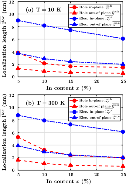
Our results as a function of the In content in the well are shown in Fig. 4 (a) for low temperatures ( K) and in (b) for room temperature ( K). Firstly, we see that carrier localization effects are still pronounced at higher carrier densities and temperatures. Comparing Fig. 3 with Fig. 4 (a) we find that the increased carrier density leads to an increase in all localization lengths. In the case of the holes this is attributable to the population of energetically higher-lying localized states (see also Appendix A for more details), whilst for the electrons the increase in length may be due to occupation of states outside of the WWF, which exhibit larger localization lengths due to the reduced (in-plane) confinement. In the absence of WWF a slight increase in the electron in-plane localization may be expected. Comparing Fig. 4 (a) with (b) we note that increasing temperature has little effect on all the localization lengths other than the in-plane hole localization (red filled circles). Interestingly, we note that for lower In contents are increased more than at higher In contents. For example, for the K case, on going from 5% to 15% In content, is reduced by a factor of order 2.2, but on going from 15% to 25%, it is reduced only by a factor of order 1.2. Thus the localization length change in the regime relevant to the green gap problem shows negligible variance when compared with lower In content regimes. We note that the general trend of a smaller change in localization effects with increasing In content has also been observed by other groups on different quantities. For instance, Piccardo et al. Piccardo et al. (2017) observed that Urbach tail energies increase strongly in the 6% to 11% In range, while for higher In contents the Urbach tail energy changes very little.
We highlight that the saturation of the hole localization length in the wavelength range relevant to the green gap (530 nm to 570 nmHammersley et al. (2015); Auf der Maur et al. (2016)), is an important result given that this quantity has generated interest as a first indicator of the deleterious effects of alloy-induced localization effects for the green gap problem. Given that there is no sudden change in the hole localization length with increasing In content/wavelenght it is unlikely to explain the sudden decrease in IQE observed (cf. Fig. 1) when going from blue to green emitters.
To extend this discussion, we note further important factors. We recall that when growing InGaN/GaN QWs with higher In contents, the growth temperature is lowered, resulting in an increase of the (point) defect density. Gür et al. (2011); Armstrong et al. (2012); Uedono et al. (2014) Point defects have been demonstrated to act as nonradiative recombination centers, which can lead to a reduction in the nonradiative recombination lifetimes. Chichibu et al. (2005); Langer et al. (2013b); Hammersley et al. (2015) Thus, the holes, whose mean localization length remains small, may remain isolated from these defects, except for those which are localized near a defect. On the other hand electrons, whose (in-plane) localization length is much larger, may now become increasingly susceptible to an increased (point) defect density. As a consequence nonradiative recombination rate may be increased. This contrasts starkly with Refs. Auf der Maur et al., 2016 and Karpov, 2017, where a constant, In content independent nonradiative recombination rate is assumed, and the reduction in devices efficiency is mainly attributed to built-in field and carrier localization effects due to random alloy fluctuations.
Finally, we note that if the carrier densities are increased further than those examined here, additional effects like field screening will come into play, and the localization lengths of especially the electrons will further increase, as we have shown in a recent work. Tanner et al. (2018) The carriers will thus become more susceptible to defects, and the aforementioned conclusions will be strengthened. In the absence of WWFs the electron localization length should increase and thus further supporting this conclusion. An interesting aspect of the above interpretation is the significant role played by the electrons, raising the question of whether it is the electrons which are the important carriers for the explanation of the green gap, rather than the holes, which have traditionally been targeted.
Having discussed the electron and hole localization lengths, we turn now to the study of the wave function overlaps. In particular, we will focus on the importance of in-plane carrier separation for the green gap problem.
III.4 Electron-hole wave function overlap
To analyze how the electron-hole wave function overlap changes with In content, without using a VCA system as a reference, we proceed as follows. In a first step, for each of the 175 different microscopic configurations per In content, the modulus electron hole wave function overlap, given by
| (5) |
has been calculated between electron state and hole state . The sum runs over all the lattice sites of the supercell. We note that our aim is to study the contribution of the in-plane carrier separation to the reduction of the total wave function overlap; radiative recombination lifetimes shall be targeted in future studies. Furthermore, we stress that our goal is to analyze the in-plane carrier separation without using a VCA as a reference, which is often done. Auf der Maur et al. (2016); Jones et al. (2017) While a comparison between an atomistic model and a VCA model would allow us, in principle, to distinguish between in- and out-of plane separation contributions (carrier localization and built-in field), this comes at cost: the magnitude and relative importance of the two different factors (built-in field and carrier localization), depend on how the parameters of the VCA calculations are are determined (linear interpolation vs. bowing parameters). Thus the absolute numbers from a comparison with VCA as a reference have to be treated with care. An approach that targets this question without a VCA will eliminate assumptions about interpolating material parameters and remove therefore an extra layer of uncertainty (over/underestimation) for the overall importance of the in-plane carrier separation for the electron-hole wave function overlap. For these reasons the modulus wave function overlap, Eq. (5), provides a coherent and consistent frame that does not suffer from assumptions made in a VCA reference frame. Also the above approach allows us in a simple manner to study the impact of the In content on the spatial separation of wave functions in InxGa1-xN/GaN QWs, both in- and out-of growth plane. In general, more details about this approach and how we have previously used it to gain insight into experimental observations such as a carrier mobility edge or the appearance of a high energy emission band can be found in Refs. Christian et al., 2018a and Blenkhorn et al., 2018, respectively. Furthermore, similar approaches have been used by other groups to study the optical properties of different nitride-based nanostructures. Marquardt et al. (2013, 2015)
Given that each electron and hole wave function is connected to a corresponding eigenenergy, one can also study an energy resolved modulus wave function overlap where is the electron eigenenergy and is the hole eigenenergy of states and , respectively. Therefore, can be visualized as a function of electron and hole energies. In a second step, the overlaps from the 175 different configurations have been grouped together in energy bins of 30 meV width. An averaged energy resolved modulus wave function overlap is obtained by dividing the sum of the overlaps in an energy bin by the number of elements therein. To better compare the results from the different In contents, the data is always plotted with respect to corresponding conduction and valence “band” edges.
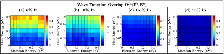
The results of this analysis are displayed in Fig. 5, with the In content increasing from left to right. Three main results may be inferred from these figures: (i) there is an overall decrease in electron and hole wave function overlap with increasing In content (and will width); (ii) for a given system, the energy range over which electrons and holes have low overlaps with each other depends on the In content; (iii) the overlap depends more weakly on the electron energy than it does on the hole energy.
Result (i) reflects mainly an increasing strain induced built-in field (which separates carriers perpendicular to the plane of the QWs, cf. Fig. 2) and alloy-fluctuation induced carrier localization (which separates carriers in-plane, cf. Fig. 2) with In content, as discussed in Sec. III.1. In our subsequent analysis we will disentangle the contribution of these two effects, as a function of the In content, in order to investigate the relevance of the alloy induced in-plane carrier separation to the green gap problem.
Point (ii) is a manifestation of an earlier reported result Tanner et al. (2016) that, not only does the strength of localization increase with In content, but so too does the energy range over which it persists (see also Appendix A for further discussion and Ref. Tanner et al. (2016)). This may have interesting consequences for the green gap, or even efficiency droop: the carrier densities and temperatures required to saturate the localized states may be higher for higher In content QWs. We will investigate this further below in the context of the green gap problem.
Aspect (iii) results from the fact that the electron localization length is large compared to that of the holes and changes little when energetically higher-lying states are populated, whilst the hole localization length increases as states deeper in the valence “band” are populated. More generally speaking, we note that this changing localization character and dependence of overlap on energy of electrons and holes away from their respective conduction or valence “band” edges is also reflected in experimental studies, for instance, in the appearance of a high energy emission band with much shorter radiative recombination times at low temperature ( K). Christian et al. (2018a)
While Fig. 5 gives first information on the evolution of the wave function overlap with In content, it does not provide information about the density of states. Therefore, to gain further insight into all three aspects discussed above, in the next steps, we include the effects of temperature and carrier density on the wave function overlaps, and investigate the specific contribution of the alloy-induced in-plane separation of carriers to the reduction of the electron-hole wave function overlap, .
First, we introduce carrier population effects due to higher temperatures and carrier densities as before using Fermi-Dirac statistics. Similarly to localization length, is defined via:
| (6) |
Here, denotes the configuration number of the different microscopic configurations per In content. The electron and hole energies are denoted by and . The factors and are the Fermi-Dirac functions for electrons and holes, respectively. The sheet carrier density for all calculations is again cm-2.
Next, we examine the contribution of the in-plane separation to the reduction of at low (T=10 K) and high (T=300 K) temperatures. For the reasons discussed above we study this question without using a VCA calculation. To achieve this unified description, we make use of the planar integrated probability density , Eq. (3). From this quantity we can determine the planar integrated (modulus) overlap . This quantity reflects what the overlap between two states would be if they were not separated from each other in the growth plane. Further discussion of this quantity and the details of its derivation are given in Appendix B. We may quantify the amount by which this is larger than , or, more meaningfully, the amount by which is reduced by in-plane carrier separation, using the following difference:
| (7) |
Thus represents the fractional reduction in the modulus overlap between electron and hole wave functions due to their in-plane separation, i.e. due to alloy and WWF induced carrier localization effects.
Figure 6 depicts the results of this analysis for the full overlap (black squares and circles) and the reduction in overlap due to in-plane separation (red squares and circles). The squares denote K (low temperature) data, while the results at K (room temperature) are given by the circles. Figure 6 reveals the general feature that with increasing In content (and well width) decreases while increases. The latter indicates an increase in in-plane carrier separation with increasing In content.
Turning specifically to the evolution of the mean full overlap (black circles and squares), which gives a first indication of how the radiative recombination rate changes with In content and temperature. Looking at the impact of temperature on the results, we see that increasing the temperature increases more for the lower In content systems than it does for the higher In content systems. This is a manifestation of this increasing energy range of localized states with increasing In content, as confirmed by Fig. 5. When increasing the temperature energetically higher lying states are populated. On average and with increased temperature, in the 5% In cases, carriers start populate more delocalized states sooner when compared to the 25% case at the same temperature and carrier density. Two important conclusions can be drawn from this for the theoretical studies of the optical properties of these structures. First, an accurate description of the density of localized states is required for accurate modeling of the radiative recombination properties. Second and connected to this, the In content plays an important role. Very high In contents may lead to an overestimation of carrier localization effects and the energy range over which localization effects are relevant. This highlights again the importance of our initial theory-experiment benchmarking exercise.
Moreover, given that is related to the radiative recombination rate, it can be seen that for instance for the 15% In case, the radiative recombination rate should increase with increasing temperature. Such an effect has been observed in the experimental study by Nippert et al. Nippert et al. (2016) However, previous theoretical studies failed to explain this behavior Jones et al. (2017) or had to include In atom clustering effects. Di Vito et al. (2019) Our results indicate the experimentally observed trend with temperature, thus highlighting that the distribution of localized states is well described by our theoretical model.
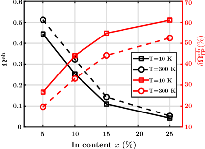
Turning to the reduction in overlap due to in-plane carrier separation, , the data clearly show that this factor increases with increasing In content. While we find that indeed in-plane carrier separation contributes strongly to the overall spatial separation of the electron and hole wave functions and is at first glance especially important in the blue to green (and even beyond) spectral range (15% to 25% In) this contribution increases only very slightly ( 10%), when compared to the composition range 5% In to 15% In ( 25%). Thus, when considering changes in the electron-hole wave function overlap with increasing In content, rather than the absolute numbers, the contribution for in-plane carrier separation emitters operating in the blue to green spectral range is not very different. This can be attributed to the situation that the distribution of localized states with energy are not vastly different over the ranges of the considered temperatures and carrier density. A further discussion is given in Appendix B. We point out that such a small change in carrier localization effects in the higher In content regime has also been observed by other groups on other quantities such as Urbach tail energies. Piccardo et al. (2017)
Finally, we note again that the argument of a smaller change in for higher In contents, when compared to the lower In content systems, would only be strengthened when keeping the well width fixed for different In contents and when neglecting WWFs. This again goes back to the situation that especially for the higher In content systems the QCSE is reduced when for instance assuming a constant well width of e.g. 3 nm. Thus for the higher In content system (25% In) the overall wave function overlap should increase, compared to the data presented for this system. Secondly, neglecting the WWFs and reducing the QCSE by reducing the well width of the here chosen 25% In structure, so that it is similar to the 15% case, the in-plane carrier localization of electrons will be reduced, which yields a reduction of the in-plane carrier separation between electrons and holes. This will lead to an overall reduction of and an even smaller change in in the 15% to 25% In content range when removing WWFs and assuming the same well width e.g. 3 nm.
Taking our results all together, it casts into doubt the idea that the observed slight change in with In content in the longer wavelength regime is the fundamental origin of the green gap problem. In other words, if the in-plane carrier separation presents a significant problem for the efficiency of InGaN-based light emitters, one could expect the drop of in efficiency to be between the near UV and the blue spectral range, with blue and green being almost equally efficient/inefficient. However, this is not observed in practice.
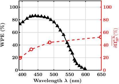
To further illustrate this point, we plot against experimental literature data on peak wall plug efficiency (WPE) values of InGaN/GaN QW structures operating in the blue to green spectral region. The experimental WPE values (black filled triangles) are shown in Fig. 7 as a function of the emission wavelength. The data has been extracted from data given in Ref. WPE, . The black line serve as a guide to the eye. For comparison we have also plotted at K as a function of the calculated emission wavelength of the InGaN/GaN QWs with different In contents. The PL peak energies originally calculated at low temperature ( K) and given in Table 1 have been adjusted by using the following correction Eliseev et al. (1997); Eliseev (2003)
| (8) |
to account for the fact that experimental data in general is obtained at room temperature ( K). denotes the energy of the PL peak energy at temperature and is the PL peak energy at K. The second term on the right-hand side corresponds to the temperature dependence of the band gap described by the Varshni equation, Vurgaftman and Meyer (2003) where and are parameters taken from Ref. Vurgaftman and Meyer, 2003; a linear interpolation between InN and GaN values has been used. The last term on the right-hand side of Eq. (8) accounts for thermal distribution of carriers between localized states. Here, is the Boltzmann constant and is connected to the red-shift of the PL peak position with temperature (“S”-shape temperature dependence). Eliseev et al. (1997); Eliseev (2003); Hammersley et al. (2012); Wang et al. (2001); Zhu et al. (2017) It should be noted that the “S”-shape temperature dependence of the PL peak energies has two red-shift regions and that Eq. (8) can only be used for the high temperature part i.e above the temperature of the maximum FWHM value. Eliseev (2003) For we have used values reported in the literature for InGaN/GaN QWs with In contents ranging from 11% to 23%. Hammersley et al. (2012); Wang et al. (2001); Zhu et al. (2017) For the studied 5% In system we have used a value of meV. Using Eq. (8) with literature -values allows us to obtain a first approximation of the emission energies at elevated temperatures . Calculating values from our data or a full PL spectrum near room temperature is beyond the scope of the present study.
Starting our analysis with the peak WPE values (black filled triangles), we observe first that the WPE is approximately constant in the nm to nm window. In contrast to this, a strong decrease in these values from a wavelength of approximately nm to nm is observed. Comparing this now with our calculated in-plane separation induced overlap reduction contribution, , we find that increases more rapidly in the nm to nm regime. However, this is the range in which the WPE is approximately constant. On the other hand the opposite behavior for WPE and is observed in the wavelength window nm, meaning that shows only a slow increase with wavelength while the WPE drops quickly. This is the opposite to what would be expected if changes in the in-plane carrier separation were the main driver behind the green gap problem. Our results suggest instead that, given the slow rate of change of , that carrier localization, and the associated in-plane separation, contributes to lesser extend to the drastic decrease in WPE. This indicates that effects other than carrier localization must contribute to the sharp reduction in WPE.
Furthermore, we note that if carrier localization effects were the origin of the green gap problem, nonpolar InGaN/GaN QW systems should not exhibit this efficiency reduction for the following reasons. Humphreys et al. (2017); Monavarian et al. (2019) With the macroscopic built-in field absent in these structures, the attractive Coulomb interaction between electrons and holes leads to exciton localization effects observed both in theory and experiment. Garrett et al. (2009); Marcinkevičius et al. (2013); Schulz et al. (2015b); Dawson et al. (2016) In a Hartree-type picture the in-plane separation between electrons and holes will be strongly reduced due to their attractive Coulomb interaction. However, as discussed by Monavarian et al. Monavarian et al. (2019), nonpolar systems do not solve the green gap problem. Obviously, nonpolar systems differ significantly in crystal quality from their polar counterparts. This indicates already that even when the in-plane carrier separation is strongly reduced in a nonpolar system compared to a polar system, the crystal quality is still very important.
While our calculations confirm that carrier localization effects and thus the associated in-plane separation effects significantly contribute to the wave function overlap reduction in -plane InGaN/GaN wells, we do not find strong changes in this quantity with changing In content in the In content range relevant for the green gap problem. Thus it cannot explain the sharp decrease in, for instance, WPE (cf. Fig. 7) We highlight again that previous theoretical studies, which assumed a constant defect related nonradiative rate, attributed carrier localization to be the main driver behind the green gap problem. Auf Der Maur and Yu Karpov (2017); Karpov (2018) Our results favor other factors such as increased point defect densities in the green spectral region and thus In content dependent nonradiative recombination pathways as the more likely explanation for the green gap problem. A similar conclusion has recently been drawn in Ref. David et al., 2019, concluding that reducing the (point) defect density could close the green gap.
IV Conclusion
In this work we have revisited the importance of carrier localization for the green gap problem. While this topic has been targeted by different groups, there remains uncertainty about the primary source of this phenomenon, and thus the best route by which it may be circumvented. As discussed above, several works impute the green gap primarily to an increased defect density, Langer et al. (2011, 2013a); David et al. (2019) while other studies focus on carrier localization effects as the main source of this effect. Nippert et al. (2016); Auf Der Maur and Yu Karpov (2017); Karpov (2018)
To shed new light onto this fundamental question we build our analysis of carrier localization effects on an atomistic multi-band tight-binding (TB) model that we rigourously benchmark against experimental data for InGaN/GaN QWs emitting over a wide range of wavelengths. These studies reveal that carrier localization effects are accurately described by our model. Quantities such as in-plane carrier separation and carrier localization lengths, originating from random alloy fluctuations, for In contents between 5% and 25% are directly calculated in an atomistic frame without fitting to experimental data.
Equipped with this model we show that carrier localization effects in InGaN QWs do not change strongly when the In content in the well is varied between 15% and 25% and thus in the emission wavelength range from to blue to green. This feature of a small change in the localization effects with In content has not been considered or discussed in works attributing the green gap problem to carrier localization; only absolute numbers were discussed in previous work rather than focussing on changes in the carrier localization effects, while also keeping the defect related nonradiative recombination rate constant with In content. Given that blue LEDs are very efficient and that the differences in alloy induced carrier localization effects do not change strongly between blue and green emitters, only slight changes to the radiative recombination rate are expected. Thus our findings cast doubt on the conclusion that the nonradiative recombination due to defects is constant and In content independent; given the small change of localization effects in the content range relevant to the green gap problem, the sharp decrease in wall plug efficiency would not be observed unless some other quantity, like defect densities, increased sharply.
We come thus to the conclusion that further factors, such as the connection between the large electron localization length and the increased defect density in the high In content regime, which could lead to reduced nonradiative carrier lifetimes, are more likely to be the driver behind the green gap problem. Experimental studies point in the same direction, although the details of the underlying mechanisms could be somewhat different. Langer et al. (2011); Hammersley et al. (2015); David et al. (2019)
Based on this explanation, accounting for the importance of the carrier (electron) localization length and increasing (point) defects densities for the green gap problem, we suggest different countermeasures. One such countermeasure is for instance the already widely used approach of underlayers. Armstrong et al. (2015b); Haller et al. (2017); Christian et al. (2018b) It has been shown that via the use of underlayers the point defect density can be reduced in the QWs, which should then be beneficial for the green gap problem. Furthermore, on the finding of a relatively large electron localization lengths and the potential connection to nonradiative recombination rate, tailoring carrier localization effects might be the way forward to close the green gap. Here, for instance co-localization of carriers by introducing quantum dot like structures in InGaN/GaN QWs could be a way forward. This would not only have the benefit of reducing the electron localization length but potentially also co-localizing electrons and holes in the same spatial region. Experimentally this might be achieved by tailoring the growth parameters (particularly the growth pressure) to induce the formation of non-random clusters in QWs that are not usually present (dot-in-well structures).
Acknowledgements.
This work was supported by Science Foundation Ireland, Sustainable Energy Authority of Ireland (project numbers 17/CDA/4789 and 13/SIRG/2210) and the United Kingdom Engineering and Physical Sciences Research Council (Grant No. EP/M010589/1).Appendix
In this appendix we provide (i) additional information about the calculation of the in-plane carrier localization length and its evolution with energy and In content for holes and (ii) further details of the in-plane carrier localization effects. In the following section, the in-plane carrier localization length will be discussed. Subsequently we discuss the in-plane carrier separation in more detail.
IV.1 Hole localization length
In the main text we have discussed the calculation of the out-of plane carrier localization length. Here we provide information about the calculation of the in-plane localization length. To evaluate the in-plane localization length , we assign a single value by use of a reference state and the underlying hexagonal crystal symmetry. We choose as our reference state the electron ground state of Config. 13 with 10% In in the well, which is shown in Fig. 2 (left). This choice is made on the basis that in-plane the electron is mainly localized within the WWF. We then associate this state with a cylindrical volume given by: , where is the radius of the WWF ( nm) and , the out-of plane localization length for the reference state. Then, utilizing the fact that the ratios of volumes occupied by two states are the same as the inverse of the ratio of their IPRs, we obtain, for a given microscopic configuration , the following expression for the in-plane localization length of a given state:
| (9) |
Here, is the full IPR value defined by Eq. (2) for our reference state discussed above (electron ground state of Config. 13; 10% In). The factor of 2 in Eq. (9) is to give the full length (diameter) of the circular geometry assumed here.
In the main text of the manuscript we have focused on the mean carrier localization length. In the following we present a detailed study of the in-plane hole localization (); the out-of plane localization length for electrons and holes is mainly dominated by the built-in field. Furthermore, we have seen in our previous work that variations in the electron IPR values are much smaller than those in the hole IPR values. Tanner et al. (2016) In what follows, we investigate the extent to which the hole in-plane localization length changes as states deeper into the valence “band” are considered, since this can give insight/indaction of the distribution of localized states in the valence “band” (density of states).
To address this point the in-plane localization length has been calculated for each of the 40 hole states in each of the 175 configurations per In content system. To plot the data from different configurations as a function of energy, the results have been collected in bins of size of 30 meV and the average localization length per bin has been calculated. A bin size of 30 meV was chosen so that it is not too large to mask any intrinsic features but not so small as to produce any empty energy bins. To compare the results between the different In contents easily, the data is always shown with respect to the respective valence “band” edge values.
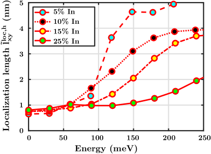
The resulting energy resolved hole in-plane localization lengths are displayed in Fig. 8. Independent of the In content, we observe that the hole in-plane localization length increases with increasing energy (moving deeper into the valence “band”). However, over an energy range of approximately 60 meV there is not a huge difference in the hole localization length at each In content. At first glance this seems to be in contradiction with Fig. 3 where the average ground state in-plane localization length is plotted and at 5% In (=3.23 eV) is larger compared to of the 25% In case (=1.99 eV). It is important to note that in Fig. 3 just averages over the ground state values are taken; this neglects any spread in the corresponding hole ground state energies. Figure 8 shows an energy resolved in-plane localization length . Therefore, one can find hole states that are as strongly localized in the 5% as in the 25% In case over the same energy range from the respective valence “band” edge. However, the density of these strongly localized states increases significantly with increasing In content. We have discussed this feature previously, Tanner et al. (2016) when studying IPR values of electronic states as a function of the state number in -plane InGaN/GaN wells with varying In contents. Furthermore, Fig. 8 reveals that the energy region over which strong localization exists increases with increasing In content. For instance, while in the 5% In case (blue filled circles, dashed line) the in-plane localization length starts to sharply increase at an energy of around 90 meV, for the 25% In case (green filled circles, solid line) we do not start to see any such increase of the in-plane localization length until hole energies exceed 210 meV.
IV.2 Wave function overlap and in-plane carrier localization
In the main text of the manuscript we have presented the contribution of in-plane separation to the reduction in the wave function overlap. Here, we provide the derivation of this quantity, and detailed results underlying above presented mean values.
To obtain , we begin with the planar integrated probability density of Eq. (3), which describes the one dimensional probability density along the -axis. We can use to calculate the planar integrated (modulus) overlap via:
| (10) |
This quantity is sensitive only to the extent to which an electron and hole wave function reside on the same plane, irrespective of whether or not they occupy the same position in that plane. This is because, based on Eq. (10), the in-plane extent of the charge density is summed up into one value per plane. Consequently, all calculations are carried out in the same frame containing the same microstructure, local strain and built-in field fluctuations as the full overlap calculations discussed above. The calculated planar integrated overlaps can again be expressed in terms of electron and hole energies and an averaged value, denoted by , which is obtained in the same manner as before for and discussed in the main text of the manuscript.
To quantify the amount by which this is larger than , or, more meaningfully, the amount by which is reduced by in-plane carrier separation, we utilize the following metric:
| (11) |
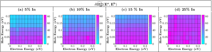
Figure 9 displays , in percent, as a function of the electron and hole energies with respect to the respective conduction and valence “band” edges.
It is apparent from the figure that in-plane separation strongly impacts the electron-hole overlaps, with percentage reductions in the overlap of up to around 80% seen for all In contents. Consistent with our results presented above on the localization lengths, the magnitude and energy range of this reduction increases with In content. For each In content, decreases with distance from the valence and conduction “band” edges, and decreases faster for lower In contents than for higher. Again, the delocalized and unchanging nature of the electron states are evidenced by the relative insensitivity of to the electron energy , when compared to the hole energy .
This significant impact of in-plane separation on the electron-hole overlap is consistent with previous works which have highlighted the negative impact of carrier localization and in-plane separation.Auf der Maur et al. (2016); Karpov (2017, 2018) However, as pointed out earlier, it is important to study changes in this quantity between blue and green emitting systems if we wish to determine its relevance to the green gap problem. If carrier localization and the associated in-plane separation were the main driver behind the green gap problem, then a strong increase in should be evident when going from the 15% to the 25% In system.
Comparing the 15% and 25% In systems, we note that differences are indeed apparent on the high-energy side of Fig. 9 (c) and (d); though, on the low energy side, these differences are less marked. The question on the importance of these differences in these energy regimes have been targeted in the main text of the manuscript.
References
- Ponce and Bour (1997) F. A. Ponce and D. Bour, Nature 386, 351 (1997).
- Akasaki and Amano (2006) I. Akasaki and H. Amano, Japanese Journal of Applied Physics 45, 9001 (2006).
- Nakamura et al. (1993) S. Nakamura, T. Mukai, M. Senoh, S. Nagahama, and N. Iwasa, Journal of Applied Physics 74, 3911 (1993).
- Mukai et al. (1999) T. Mukai, M. Yamada, and S. Nakamura, Japanese Journal of Applied Physics 38, 3976 (1999).
- Humphreys (2008) C. J. Humphreys, MRS Bulletin 33, 459 (2008).
- Krames et al. (2007) M. R. Krames, O. B. Shchekin, R. Mueller-Mach, G. O. Mueller, L. Zhou, G. Harbers, and M. G. Craford, Journal of Display Technology 3, 160 (2007).
- Karpov (2016) S. Y. Karpov, Proc. SPIE 9768, 9768 (2016).
- Crawford (2009) M. H. Crawford, IEEE Journal of Selected Topics in Quantum Electronics 15, 1028 (2009).
- Langer et al. (2013a) T. Langer, H. Jönen, A. Kruse, H. Bremers, U. Rossow, and A. Hangleiter, Applied Physics Letters 103, 022108 (2013a).
- Armstrong et al. (2012) A. Armstrong, T. A. Henry, D. D. Koleske, M. H. Crawford, and S. R. Lee, Opt. Express 20, A812 (2012).
- Massabuau et al. (2014) F. C.-P. Massabuau, M. J. Davies, F. Oehler, S. K. Pamenter, E. J. Thrush, M. J. Kappers, A. Kovacs, T. Williams, M. A. Hopkins, C. J. Humphreys, P. Dawson, R. E. Dunin-Borkowski, J. Etheridge, D. W. E. Allsopp, and R. A. Oliver, Appl. Phys. Lett. 105, 112110 (2014).
- Uedono et al. (2014) A. Uedono, S. Ishibashi, N. Oshima, R. Suzuki, and M. Sumiya, ECS Trans 61, 19 (2014).
- Hammersley et al. (2015) S. Hammersley, M. J. Kappers, F. C. P. Massabuau, S.-L. Sahonta, P. Dawson, R. A. Oliver, and C. J. Humphreys, J. Appl. Phys. 107, 132106 (2015).
- Langer et al. (2011) T. Langer, A. Kruse, F. A. Ketzer, A. Schwiegel, L. Hoffmann, H. Jönen, H. Bremers, U. Rossow, and A. Hangleiter, physica status solidi c 8, 2170 (2011).
- Armstrong et al. (2015a) A. M. Armstrong, B. N. Bryant, M. H. Crawford, D. D. Koleske, S. R. Lee, and J. J. Wierer, J. Appl. Phys. 117, 134501 (2015a).
- Zhu et al. (2017) Y. Zhu, T. Lu, X. Zhou, G. Zhao, H. Dong, Z. Jia, X. Liu, and B. Xu, Nanoscale Research Letters 12, 321 (2017).
- Tian et al. (2017) A. Tian, J. Liu, L. Zhang, Z. Li, M. Ikeda, S. Zhang, D. Li, P. Wen, F. Zhang, Y. Cheng, X. Fan, and H. Yang, Opt. Express 25, 415 (2017).
- Ambacher et al. (2002) O. Ambacher, J. Majewski, C. Miskys, A. Link, M. Hermann, M. Eickhoff, M. Stutzmann, F. Bernardini, V. Fiorentini, V. Tilak, B. Schaff, and L. F. Eastman, J. Phys.: Condens. Matter 14, 3399 (2002).
- Patra and Schulz (2017) S. K. Patra and S. Schulz, Phys. Rev. B 96, 155307 (2017).
- Andreev and O’Reilly (2001) A. D. Andreev and E. P. O’Reilly, Appl. Phys. Lett. 79, 521 (2001).
- Yang et al. (2014) T.-J. Yang, R. Shivaraman, J. S. Speck, and Y.-R. Wu, J. Appl. Phys. 116, 113104 (2014).
- Auf der Maur et al. (2016) M. Auf der Maur, A. Pecchia, G. Penazzi, W. Rodrigues, and A. Di Carlo, Phys. Rev. Lett. 116, 027401 (2016).
- Jones et al. (2017) C. M. Jones, C.-H. Teng, Q. Yan, P.-C. Ku, and E. Kioupakis, Appl. Phys. Lett. 111, 113501 (2017).
- Karpov (2017) S. Y. Karpov, Photonics Research 5, A7 (2017).
- Karpov (2018) S. Y. Karpov, Appl. Sci. 8, 818 (2018).
- Nippert et al. (2016) F. Nippert, S. Y. Karpov, G. Callsen, B. Galler, T. Kure, C. Nenstiel, M. R. Wagner, M. Straßburg, H.-J. Lugauer, and A. Hoffmann, Appl. Phys. Lett. 109, 161103 (2016).
- Watson-Parris et al. (2011) D. Watson-Parris, M. J. Godfrey, P. Dawson, R. A. Oliver, M. J. Galtrey, M. J. Kappers, and C. J. Humphreys, Phys. Rev. B 83, 115321 (2011).
- David et al. (2019) A. David, N. G. Young, C. A. Hurni, and M. D. Craven, Phys. Rev. Appl. 11, 031001 (2019).
- Auf Der Maur and Yu Karpov (2017) M. Auf Der Maur and S. Yu Karpov, Compund Semiconductor 23, 28 (2017).
- Chichibu et al. (2006) S. F. Chichibu, A. Uedono, T. Onuma, B. A. Haskell, A. Chakraborty, T. Koyama, P. T. Fini, S. Keller, S. P. DenBaars, J. S. Speck, U. K. Mishra, S. Nakamura, S. Yamaguchi, S. Kamiyama, H. Amano, I. Akasaki, J. Han, and T. Sota, Nature Mater. 5, 810 (2006).
- Dawson et al. (2016) P. Dawson, S. Schulz, R. A. Oliver, M. J. Kappers, and C. J. Humphreys, J. Appl. Phys. 119, 181505 (2016).
- Haller et al. (2017) C. Haller, J.-F. Carlin, G. Jacopin, D. Martin, R. Butte, and N. Grandjean, Appl. Phys. Lett. 111, 262101 (2017).
- Graham et al. (2005) D. M. Graham, A. Soltani-Vala, P. Dawson, M. J. Godfrey, T. M. Smeeton, J. S. Barnard, M. J. Kappers, C. J. Humphreys, and E. J. Thrush, J. Appl. Phys. 97, 103508 (2005).
- Watson-Parris (2011) D. T. S. Watson-Parris, Carrier Localization in InGaN/GaN Quantum Wells, PhD Thesis University of Manchester (https://www.escholar.manchester.ac.uk/uk-ac-man-scw:132844, 2011).
- Caro et al. (2013) M. A. Caro, S. Schulz, and E. P. O’Reilly, Phys. Rev. B 88, 214103 (2013).
- O’Reilly et al. (2002) E. P. O’Reilly, A. Lindsay, S. Tomic, and M. Kamal-Saadi, Semicond. Sci. Technol. 17, 870 (2002).
- Li and Pötz (1992) Z. Q. Li and W. Pötz, Phys. Rev. B 46, 2109 (1992).
- Boykin et al. (2007) T. B. Boykin, N. Kharche, G. Klimeck, and M. Korkusinski, J. Phys.: Condens. Matter 19, 036203 (2007).
- Williams et al. (2005) D. P. Williams, A. D. Andreev, E. P. O’Reilly, and D. A. Faux, Phys. Rev. B 72, 235318 (2005).
- Schulz et al. (2015a) S. Schulz, M. A. Caro, C. Coughlan, and E. P. O’Reilly, Phys. Rev. B 91, 035439 (2015a).
- Schulz et al. (2015b) S. Schulz, D. P. Tanner, E. P. O’Reilly, M. A. Caro, T. L. Martin, P. A. J. Bagot, M. P. Moody, F. Tang, J. T. Griffiths, F. Oehler, M. J. Kappers, R. A. Oliver, C. J. Humphreys, D. Sutherland, M. J. Davies, and P. Dawson, Phys. Rev. B 92, 235419 (2015b).
- Patra et al. (2017) S. K. Patra, T. Wang, T. J. Puchtler, T. Zhu, R. A. Oliver, R. A. Taylor, and S. Schulz, Phys. Status Solidi B 254, 1600675 (2017).
- Tanner et al. (2018) D. S. P. Tanner, J. M. McMahon, and S. Schulz, Phys. Rev. Applied 10, 034027 (2018).
- Schulz et al. (2006) S. Schulz, S. Schumacher, and G. Czycholl, Phys. Rev. B 73, 245327 (2006).
- Monemar et al. (2002) B. Monemar, P. P.Paskov, J. P. Bergman, G. Pozina, V. Darakchieva, M. Iwaya, S. Kamiyama, H. Amano, and I. Akasaki, MRS Internet J. Nitride Semicond. Res. 7, 7 (2002).
- O’Neill et al. (2003) J. P. O’Neill, I. M. Ross, A. G. Cullis, T. Wang, and P. J. Parbrook, Applied Physics Letters 83, 1965 (2003).
- Smeeton et al. (2003) T. M. Smeeton, M. J. Kappers, J. S. Barnard, M. E. Vickers, and C. J. Humphreys, Appl. Phys. Lett. 83, 5419 (2003).
- Galtrey et al. (2008) M. J. Galtrey, R. A. Oliver, M. J. Kappers, C. J. Humphreys, P. Clifton, D. Larson, D. Saxey, and A. Cerezo, J. Appl. Phys. 104, 013524 (2008).
- Tanner et al. (2016) D. P. Tanner, M. A. Caro, E. P. O’Reilly, and S. Schulz, RSC Adv. 6, 64513 (2016).
- Piccardo et al. (2017) M. Piccardo, C.-K. Li, Y.-R. Wu, J. S. Speck, B. Bonef, R. M. Farrell, M. Filoche, L. Martinelli, J. Peretti, and C. Weisbuch, Phys. Rev. B 95, 144205 (2017).
- Massabuau et al. (2017) F. Massabuau, N. Piot, M. Frentrup, X. Wang, Q. Avenas, M. Kappers, C. Humphreys, and R. Oliver, Phys. Status Solidi B 254, 1600664 (2017).
- Morel et al. (2003) A. Morel, P. Lefebvre, S. Kalliakos, T. Taliercio, T. Bretagnon, and B. Gil, Phys. Rev. B 68, 045331 (2003).
- Di Vito et al. (2019) A. Di Vito, A. Pecchia, A. Di Carlo, and M. Auf der Maur, Phys. Rev. Applied 12, 014055 (2019).
- Robin et al. (2018) Y. Robin, M. Pristovsek, H. Amano, F. Oehler, R. A. Oliver, and C. J. Humphreys, J. Appl. Phys. 124, 183102 (2018).
- Thouless (1974) D. J. Thouless, Physics Reports 13, 93 (1974).
- Wegner (1980) F. Wegner, Z. Physik B 36, 209 (1980).
- Ludwig et al. (2003) H. Ludwig, E. Runge, and R. Zimmermann, Phys. Rev. B 67, 205302 (2003).
- Chan et al. (2010) J. A. Chan, J. Z. Liu, and A. Zunger, Phys. Rev. B 82, 045112 (2010).
- Christian et al. (2018a) G. M. Christian, S. Schulz, M. J. Kappers, C. J. Humphreys, R. A. Oliver, and P. Dawson, Phys. Rev. B 98, 155301 (2018a).
- Wu et al. (2009) Y.-R. Wu, Y.-Y. Lin, H.-H. Huang, and J. Singh, J. Appl. Phys. 105, 013117 (2009).
- Gür et al. (2011) E. Gür, Z. Zhang, S. Krishnamoorthy, S. Rajan, and S. A. Ringe, Appl. Phys. Lett. 99, 092109 (2011).
- Chichibu et al. (2005) S. F. Chichibu, A. Uedono, T. Onuma, T. Sota, B. A. Haskell, S. P. DenBaars, J. S. Speck, and S. Nakamura, Appl. Phys. Lett. 86, 021914 (2005).
- Langer et al. (2013b) T. Langer, H.-G. Pietscher, H. Bremers, U. Rossow, D. Menzel, and A. Hangleiter, Proc. SPIE 8625, 862522 (2013b).
- Blenkhorn et al. (2018) W. E. Blenkhorn, S. Schulz, D. S. P. Tanner, R. A. Oliver, M. J. Kappers, C. J. Humphreys, and P. Dawson, J. Phys.: Condens. Matter 30, 175303 (2018).
- Marquardt et al. (2013) O. Marquardt, C. Hauswald, M. Wölz, L. Geelhaar, and O. Brandt, Nano Lett. 13, 3298 (2013).
- Marquardt et al. (2015) O. Marquardt, L. Geelhaar, and O. Brandt, Nano Lett. 15, 4289 (2015).
- (67) “Closing the green gap, howpublished = https://www.energy.gov/sites/prod/files/2019/02/f59/hahn-gap_ssl-rd2019.pdf, note = Accessed: 2019-12-10,” .
- Eliseev et al. (1997) P. G. Eliseev, P. Perlin, J. Lee, and M. Osinski, Appl. Phys. Lett. 71, 569 (1997).
- Eliseev (2003) P. G. Eliseev, J. Appl. Phys. 93, 5404 (2003).
- Vurgaftman and Meyer (2003) I. Vurgaftman and J. R. Meyer, J. Appl. Phys. 94, 3675 (2003).
- Hammersley et al. (2012) S. Hammersley, D. Watson-Parris, P. Dawson, M. J. Godfrey, T. J. Badcock, M. J. Kappers, C. McAleese, R. A. Oliver, and C. J. Humphreys, J. Appl. Phys. 111, 083512 (2012).
- Wang et al. (2001) T. Wang, J. Bai, and S. Sakai, J. Cryst. Growth 224, 5 (2001).
- Humphreys et al. (2017) C. J. Humphreys, J. T. Griffiths, F. Tang, F. Oehler, S. D. Findlay, C. Zheng, J. Etheridge, T. L.Martin, P. A. J. Bagot, M. P. Moody, D. Sutherland, P. Dawson, S. Schulz, S.Zhang, W. Y. Fu, T. Zhu, M. J. Kappers, and R. A. Oliver, Ultramicroscopy 176, 93 (2017).
- Monavarian et al. (2019) M. Monavarian, A. Rashidi, and D. Feezell, Phys. Status Solidi A 216, 1800628 (2019).
- Garrett et al. (2009) G. A. Garrett, H. Shen, M. Wraback, A. Tyagi, M. C. Schmidt, J. S. Speck, S. P. DenBaars, and S. Nakamaura, Phys. Stat. Solidi (c) 6, S800 (2009).
- Marcinkevičius et al. (2013) S. Marcinkevičius, K. M. Kelchner, L. Y. Kuritzky, S. Nakamura, S. P. DenBaars, and J. S. Speck, Appl. Phys. Lett. 103, 111107 (2013).
- Armstrong et al. (2015b) A. M. Armstrong, B. N. Bryant, M. H. Crawford, D. D. Koleske, S. R. Lee, and J. J. W. Jr., J. Appl. Phys. 117, 134501 (2015b).
- Christian et al. (2018b) G. Christian, M. Kappers, F. Massabuau, C. Humphreys, R. Oliver, and P. Dawson, Materials 9, 1736 (2018b).