High coherence superconducting microwave cavities with indium bump bonding
Abstract
Low-loss cavities are important in building high-coherence superconducting quantum computers. Generating high quality joints between parts is crucial to the realization of a scalable quantum computer using the circuit quantum electrodynamics (cQED) framework. In this paper, we adapt the technique of indium bump bonding to the cQED architecture to realize high quality superconducting microwave joints between chips. We use this technique to fabricate compact superconducting cavities in the multilayer microwave integrated quantum circuits (MMIQC) architecture and achieve single photon quality factor over 300 million or single-photon lifetimes approaching 5 ms. To quantify the performance of the resulting seam, we fabricate microwave stripline resonators in multiple sections connected by different numbers of bonds, resulting in a wide range of seam admittances. The measured quality factors combined with the designed seam admittances allow us to bound the conductance of the seam at . Such a conductance should enable construction of micromachined superconducting cavities with quality factor of at least a billion. These results demonstrate the capability to construct very high quality microwave structures within the MMIQC architecture.
I introduction
Circuit quantum electrodynamics (cQED) is one of the most promising platforms for quantum computation. Coherence times have been dramatically improved in the past decade Kjaergaard et al. (2019). Additionally, circuits with dozens of qubits have been realized and used to demonstrate many interesting results, such as molecular simulations Wang et al. (2019); Kandala et al. (2019); O’Malley et al. (2016), condensed matter simulations Ma et al. (2019), and proof-of-principle quantum supremacy calculations Arute et al. (2019). However, further scaling up the number of circuit components while maintaining or even improving their coherence is very challenging.
In the past several years, techniques from the MEMS industry have been applied to the cQED platform to construct multilayer microwave integrated quantum circuits (MMIQC) Brecht et al. (2016). Tremendous progress has been achieved in 3D integration of quantum circuit elements while maintaining their coherence Rosenberg et al. (2017); Dunsworth et al. (2017a); Brecht et al. (2015, 2017). Micromachined superconducting cavities can be highly useful in the MMIQC architecture. Such structures can serve as long-lived quantum memories or as enclosures to suppress radiation loss to the environment and crosstalk between quantum circuit elements. A crucial requirement for constructing high quality micromachined superconducting cavities is the fabrication of high quality microwave joints between layers of the MMIQC Brecht et al. (2015). The loss associated with joints significantly limits the choice of geometry and materials of the superconducting cavity, as well as the layout of quantum circuits. To maintain the performance of superconducting cavities without sacrificing design flexibility, reducing the loss associated with the joints is critically important.
In this work, we adapt indium bump bonding to the cQED architecture. Using this technique, we create superconducting joints with very low loss at microwave frequency. In Sec. 2, we quantify the loss of the resulting joint by fabricating bump-bonded indium stripline resonators and measuring their internal quality factors. In Sec. 3 we apply this indium bump-bonding technique to realize high quality micromachined cavities and show devices with low-power quality factor of over 300 million.
II Ultra-low loss joints with indium bump bonding
Building superconducting cavities requires joining together at least two different parts. However, the seam at the joint may limit the coherence of a cavity resonator. In an ideal joint, the contact surfaces participating in the seam would be identical to the bulk material that comprises the remainder of the cavity; there would be no extra loss associated with the seam. In a realistic joint, imperfections such as lattice defects, metal oxides, or organic residue on the surfaces can reduce the electrical conductivity across seam and degrade the quality of the resonator. The loss of the seam can be quantified with the following phenomenological model from Brecht et al. (2015):
| (1) |
where is a unit vector along the seam, and the integral in the denominator is taken over the entire volume of the mode. The conductance per unit length is an empirical value, and the admittance per unit length is a geometric factor that can be calculated analytically or numerically.
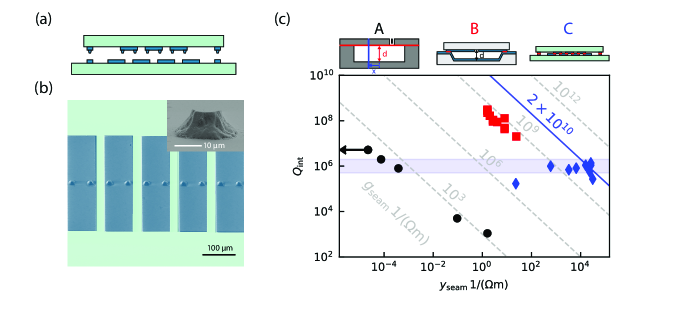
Previous studies Brecht et al. (2015) have shown that seam loss can be dominant in a cavity, depending on cavity geometry and location as well as quality of the seam, as shown in Fig. 1(c). Series A (black circles, data taken from Brecht et al. (2015)) represents the TE110 modes of a set of rectangular cavity resonators machined out of bulk 6061 aluminum. Each device is nominally identical, except for the location of its seam. The different seam positions result in different values of , with higher corresponding to lower . The internal quality factors of these devices lie on a diagonal line corresponding to a . Since the geometries of the devices are nominally identical, the energy participation in other loss mechanisms remains fixed while the varies. This is consistent with their Q’s being limited by the seam loss. For micromachined superconducting cavities made by bonding two wafers together, the location of the joint is at the worst location for the fundamental mode, with . In order to improve its coherence time, it is therefore necessary to increase the by developing better joints.
An ideal joint would have both low electrical loss at microwave frequencies and mechanical stability at cryogenic temperatures. Indium bump bonding is an established method that has been used in the field of cryogenic detectors DeNigris et al. (2018), and has several properties that make it a good candidate for an ultra-low loss joint for superconducting quantum computing applications. Indium cold welds to itself and is not brittle at cryogenic temperatures Datta et al. (2004), allowing for room-temperature bonding which remains robust even with thermal cycling to milli-Kelvin temperatures. Additionally, indium superconducts at 3.4 K and can thus form low-loss bonds. Finally, it is compatible with standard lithographic techniques, enabling the adaptation of existing approaches for scaling up quantum circuits. Recently, indium bonding has been used for chip hybridization and interconnections Foxen et al. (2017); Rosenberg et al. (2017); O’Brien et al. (2017); McRae et al. (2017). In this work, we optimize the existing bonding technique to attain ultra-low loss joints in the microwave frequency range.
We fabricate indium bumps using a variant of the standard process (see supplement for more details). Photolithography is used to lift off thermally evaporated indium, forming approximately bumps (see inset in Fig. 1(b)). For the other side of the joint, we leave a uniform layer of evaporated indium. Before bonding, we treat both chips with a plasma surface treatment in order to remove oxide and passivate the surface. Finally, we bond the two chips in a commercial wafer bonder at room temperature.
In order to characterize the quality of the resulting joint, we create indium stripline resonators in multiple sections connected by varying numbers of bump bonds (see Fig. 1(a)). By varying the number of bumps, we can change the of the devices. The highest is achieved when there are the maximum number of bumps given fabrication constraints (see Fig. 1(b)). These devices can attain much higher than micromachined cavities without too much of a decrease in Q, allowing us to place a tighter lower bound on . A control device is also created by placing the entire stripline on one chip, which is still bonded to the second chip by the mechanical support bumps on the edge. Since such a device has no seam at all, its should be precisely 0.
We measure the stripline resonators in a multiplexed package in hanger configuration at the base of a dilution refrigerator, with temperature around 15 mK Axline et al. (2016). Series C (blue diamonds) in Fig. 1(c) represents these devices. A shaded blue band is drawn around the control device with width set by normal variation between devices. We note that most of the devices lie within this band, except for two with lower Q, which could be caused by some imperfection in the device or the bond. This indicates that the measured Q factors of the bump-bonded resonators are not limited by the seam loss and are instead limited by other mechanisms, such as dielectric or conductor losses. With these data we can place a lower bound on , which is representative of the distribution of several points around our highest . A seam with such a conductance would enable a micromachined cavity to have Q of 1-10 billion, depending on depth.
III High-quality superconducting micromachined cavities
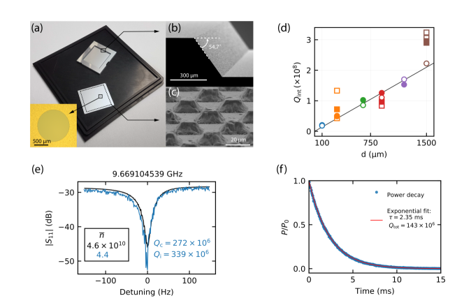
The high-quality indium joint can be applied to enhance the lifetime of a superconducting cavity resonator. In this section, we apply the indium bump bonding technique described in the previous section to construct high-quality micromachined cavities. The cavities are composed of two silicon chips that are metallized with of thermally evaporated indium (Fig. 2a). The bottom chip contains a rectangular recess area made using a potassium hydroxide anisotropic silicon etch, resulting in a sidewall (Fig. 2b). The top chip is patterned with a coupling aperture for measurement (inset in Fig. 2a). In order to improve the seam quality, indium bump arrays are fabricated along the contact region on the top chip (dashed line on the top chip in Fig. 2a). The two chips are bonded together with a commercial wafer bonder with a force of in ambient conditions to form a micromachined cavity, which is mounted on a sample holder to be measured in a reflection configuration (see supplementary materials for more details).
The internal loss of the micromachined cavity consists of the conductive loss of the indium, the dielectric loss of the indium oxide, and the loss from the seam formed at the contact of the two chips
| (2) |
Here, is the frequency of the cavity resonance, is the vacuum permeability, and is the penetration depth of indium. The kinetic inductance fraction , the surface dielectric participation ratio , and the seam admittance per unit length are geometrical parameters that can be calculated analytically or numerically. The surface resistance of the superconductor, the loss tangent of the surface dielectric, and the seam conductance per unit length represent the intrinsic loss of each respective loss mechanism.
For the TE110 mode of the micromachined cavity, we observe that the internal quality factor increases linearly with , as shown in Fig. 2(d). However, for this mode , , and are all inversely proportional to the depth of the cavity . Therefore, we cannot determine which loss mechanisms are dominant based on this set of measurements. Nevertheless, by attributing the total loss to a single loss mechanism, we can place bounds on the corresponding intrinsic loss, which gives , , and . The highest internal quality factor we have achieved in this study is with cavity depth . The lifetimes of these cavities are independent of whether a phase-sensitive heterodyne measurement (Fig. 2(e)) or a phase-insensitive power ringdown measurement (Fig. 2(f)) is used, i.e., . No apparent degradation in internal quality factor has been observed after the samples have been exposed to air for over 3 months.
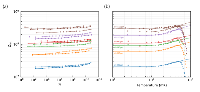
As in other 3D superconducting cavity resonators, the internal quality factors of the micromachined cavities depend very weakly on the average photon number . We observed an increase of less than from several to 10 billion photons (see Fig. 3(a)). This represents a marked difference from coplanar waveguide (CPW) resonators, the internal quality factors of which typically increase by more than a factor of two from one to photons Pappas et al. (2011); Quintana et al. (2014); Bruno et al. (2015); Calusine et al. (2018), at which point the increase becomes saturated by the power-independent losses. This power-dependent behavior of the internal quality factor of superconducting microwave resonators is generally believed to be caused by the saturation of the two-level system (TLS) dissipators by the electric field of the resonator. These TLS’s are believed to be hosted by the surface dielectrics of the resonator Gao (2008); Pappas et al. (2011). The resulting power- and temperature-dependent surface dielectric loss tangent is given by
| (3) |
where is the Boltzmann constant and is the loss tangent of the TLS dissipators at zero temperature and zero electric field. The critical photon number is the minimum number of photons required to saturate the TLS loss. For typical aluminum CPW resonators, Quintana et al. (2014); Dunsworth et al. (2017b), which is determined by the properties of the TLS’s in the hosted material as well as the electric field-weighted mode volume of the resonance . Assuming that the dipole moment and the coherence time of the TLS’s remain unchanged, . We note that the mode volume of a micromachined cavity is several million times larger than that of a CPW resonator. As shown in Fig. 3(a), of the micromachined cavities starts to increase around photons, i.e., . Therefore, the ratio is about the same for CPW resonators and micromachined cavities, suggesting that the TLS properties are similar for aluminum and indium surfaces.
In addition, the TLS dissipators can be saturated by thermal excitations, as can be seen in Eq.(3). As the temperature increases, the of the micromachined cavities rises and is maximized at , then drops due to the increase of broken Cooper pairs, (see Fig. 3(b)). This temperature-dependent behavior indicates that TLS loss is one of the dominant loss channels in these cavities. Assuming the TLS dissipators are homogeneously distributed within a thin dielectric layer on the surface of the micromachined cavities, the internal loss of the cavities can be expressed as the sum of the temperature-independent loss and the temperature-dependent TLS loss via
| (4) |
here we consider and , with the superconducting transition temperature for indium. The solid curves in Fig. 3(b) are the fit with E.q. (4) assuming a -thick dielectric layer with , which gives on the indium surface. This is similar to the loss tangent of the TLS dissipators found on aluminum oxide, which have Pappas et al. (2011); McRae et al. (2019).
IV Conclusion and perspectives
In this work, we have demonstrated techniques to fabricate and characterize high-quality superconducting joints. We have used the bump-bonding technique to construct high quality indium micromachined cavities using industry standard techniques that do not require manual assembly and is fully compatible with existing Josephson junction fabrication processes. We have achieved a low-power internal quality factor of over 300 million corresponding to an intrinsic T1 approaching 5 ms, which is comparable to the performance of conventionally machined cavities used for quantum memories in cQED. This result together with the ability to make low-loss joints shows that indium is a good superconductor for making high-quality quantum circuits. Integration of a micromachined cavity with a qubit has been demonstrated Brecht et al. (2017); by applying the techniques developed here we can improve the lifetime of a MMIQC-based quantum memory to the millisecond level.
The desire to build 3D cavities either to serve as quantum memories or to provide electromagnetic shielding highlights the fact that seam losses are very important for the 3D integration of quantum circuits. Since the scaling of superconducting circuits for quantum information processing will likely require multilayer circuits and interconnects Brecht et al. (2017); Rosenberg et al. (2017), the improved performance of the superconducting joints demonstrated here can be a key enabler for enhancing coherence in a wide range of devices. It also allows the realization of low-loss compact multilayer circuits including flip-chip resonators and lumped-element microwave networks.
This work thus provides an important step towards building a more complicated MMIQC while improving its performance.
V Acknowledgements
We thank Harvey Moseley, Ari Brown, Nicholas Costen, Timothy Miller, and Luke Burkhart, and Gianluigi Catelani for useful conversations; Jan Schroers and Teresa Brecht for assistance with wafer bonding; Charles Ahn, Frederick Walker, and Cristina Visani for assistance with DC measurements of our indium films; Philip Reinhold and Christopher Axline for experimental assistance; Michael Power, Michael Rooks, Christopher Tillinghast, James Agresta, Yong Sun, Sean Rinehart, and Kelley Woods for assistance with device fabrication. This research was supported by the U.S. Army Research Office grant W911NF-18-1-0212. S. G. was supported by a Max Planck Research Award from the Alexander von Humboldt Foundation. Facilities use was supported by the Yale university cleanroom and YINQE.
References
- Kjaergaard et al. (2019) M. Kjaergaard, M. E. Schwartz, J. Braumüller, P. Krantz, J. I.-J. Wang, S. Gustavsson, and W. D. Oliver, Superconducting qubits: Current state of play, arXiv preprint arXiv:1905.13641 (2019).
- Wang et al. (2019) C. S. Wang, J. C. Curtis, B. J. Lester, Y. Zhang, Y. Y. Gao, J. Freeze, V. S. Batista, P. H. Vaccaro, I. L. Chuang, L. Frunzio, et al., Quantum simulation of molecular vibronic spectra on a superconducting bosonic processor, arXiv preprint arXiv:1908.03598 (2019).
- Kandala et al. (2019) A. Kandala, K. Temme, A. D. Córcoles, A. Mezzacapo, J. M. Chow, and J. M. Gambetta, Error mitigation extends the computational reach of a noisy quantum processor, Nature 567, 491 (2019).
- O’Malley et al. (2016) P. J. O’Malley, R. Babbush, I. D. Kivlichan, J. Romero, J. R. McClean, R. Barends, J. Kelly, P. Roushan, A. Tranter, N. Ding, et al., Scalable quantum simulation of molecular energies, Physical Review X 6, 031007 (2016).
- Ma et al. (2019) R. Ma, B. Saxberg, C. Owens, N. Leung, Y. Lu, J. Simon, and D. I. Schuster, A dissipatively stabilized mott insulator of photons, Nature 566, 51 (2019).
- Arute et al. (2019) F. Arute, K. Arya, R. Babbush, D. Bacon, J. C. Bardin, R. Barends, R. Biswas, S. Boixo, F. G. Brandao, D. A. Buell, et al., Quantum supremacy using a programmable superconducting processor, Nature 574, 505 (2019).
- Brecht et al. (2016) T. Brecht, W. Pfaff, C. Wang, Y. Chu, L. Frunzio, M. H. Devoret, and R. J. Schoelkopf, Multilayer microwave integrated quantum circuits for scalable quantum computing, npj Quantum Information 2, 16002 (2016).
- Rosenberg et al. (2017) D. Rosenberg, D. Kim, R. Das, D. Yost, S. Gustavsson, D. Hover, P. Krantz, A. Melville, L. Racz, G. Samach, et al., 3d integrated superconducting qubits, npj quantum information 3, 42 (2017).
- Dunsworth et al. (2017a) A. Dunsworth, A. Megrant, R. Barends, Y. Chen, Z. Chen, B. Chiaro, A. Fowler, B. Foxen, E. Jeffrey, J. Kelly, et al., Low loss multi-layer wiring for superconducting microwave devices, arXiv preprint arXiv:1712.01671 (2017a).
- Brecht et al. (2015) T. Brecht, M. Reagor, Y. Chu, W. Pfaff, C. Wang, L. Frunzio, M. H. Devoret, and R. J. Schoelkopf, Demonstration of superconducting micromachined cavities, Applied Physics Letters 107, 192603 (2015).
- Brecht et al. (2017) T. Brecht, Y. Chu, C. Axline, W. Pfaff, J. Z. Blumoff, K. Chou, L. Krayzman, L. Frunzio, and R. J. Schoelkopf, Micromachined integrated quantum circuit containing a superconducting qubit, Physical Review Applied 7, 044018 (2017).
- DeNigris et al. (2018) N. DeNigris, J. Chervenak, S. Bandler, M. Chang, N. Costen, M. Eckart, J. Ha, C. Kilbourne, and S. Smith, Fabrication of flexible superconducting wiring with high current-carrying capacity indium interconnects, Journal of Low Temperature Physics 193, 687 (2018).
- Datta et al. (2004) M. Datta, T. Osaka, and J. W. Schultze, Microelectronic packaging (CRC press, 2004).
- Foxen et al. (2017) B. Foxen, J. Mutus, E. Lucero, R. Graff, A. Megrant, Y. Chen, C. Quintana, B. Burkett, J. Kelly, E. Jeffrey, et al., Qubit compatible superconducting interconnects, arXiv preprint arXiv:1708.04270 (2017).
- O’Brien et al. (2017) W. O’Brien, M. Vahidpour, J. T. Whyland, J. Angeles, J. Marshall, D. Scarabelli, G. Crossman, K. Yadav, Y. Mohan, C. Bui, et al., Superconducting caps for quantum integrated circuits, arXiv preprint arXiv:1708.02219 (2017).
- McRae et al. (2017) C. McRae, J. Béjanin, Z. Pagel, A. Abdallah, T. McConkey, C. Earnest, J. Rinehart, and M. Mariantoni, Thermocompression bonding technology for multilayer superconducting quantum circuits, Applied Physics Letters 111, 123501 (2017).
- Axline et al. (2016) C. Axline, M. Reagor, R. Heeres, P. Reinhold, C. Wang, K. Shain, W. Pfaff, Y. Chu, L. Frunzio, and R. J. Schoelkopf, An architecture for integrating planar and 3d cqed devices, Applied Physics Letters 109, 042601 (2016).
- Pappas et al. (2011) D. P. Pappas, M. R. Vissers, D. S. Wisbey, J. S. Kline, and J. Gao, Two level system loss in superconducting microwave resonators, IEEE Transactions on Applied Superconductivity 21, 871 (2011).
- Quintana et al. (2014) C. Quintana, A. Megrant, Z. Chen, A. Dunsworth, B. Chiaro, R. Barends, B. Campbell, Y. Chen, I.-C. Hoi, E. Jeffrey, et al., Characterization and reduction of microfabrication-induced decoherence in superconducting quantum circuits, Applied Physics Letters 105, 062601 (2014).
- Bruno et al. (2015) A. Bruno, G. De Lange, S. Asaad, K. Van der Enden, N. Langford, and L. DiCarlo, Reducing intrinsic loss in superconducting resonators by surface treatment and deep etching of silicon substrates, Applied Physics Letters 106, 182601 (2015).
- Calusine et al. (2018) G. Calusine, A. Melville, W. Woods, R. Das, C. Stull, V. Bolkhovsky, D. Braje, D. Hover, D. K. Kim, X. Miloshi, et al., Analysis and mitigation of interface losses in trenched superconducting coplanar waveguide resonators, Applied Physics Letters 112, 062601 (2018).
- Gao (2008) J. Gao, The physics of superconducting microwave resonators, Ph.D. thesis, California Institute of Technology (2008).
- Dunsworth et al. (2017b) A. Dunsworth, A. Megrant, C. Quintana, Z. Chen, R. Barends, B. Burkett, B. Foxen, Y. Chen, B. Chiaro, A. Fowler, et al., Characterization and reduction of capacitive loss induced by sub-micron josephson junction fabrication in superconducting qubits, Applied Physics Letters 111, 022601 (2017b).
- McRae et al. (2019) C. McRae, R. Lake, J. Long, M. Bal, X. Wu, B. Jugdersuren, T. Metcalf, X. Liu, and D. Pappas, Dielectric loss extraction for superconducting microwave resonators, arXiv preprint arXiv:1909.07428 (2019).