Impact of surface roughness in nanogap plasmonic systems
Abstract
Recent results have shown unprecedented control over separation distances between two metallic elements hundreds of nanometers in size, underlying the effects of free-electron nonlocal response also at mid-infrared wavelengths. Most of metallic systems however, still suffer from some degree of inhomogeneity due to fabrication-induced surface roughness. Nanoscale roughness in such systems might hinder the understanding of the role of microscopic interactions. Here we investigate the effect of surface roughness in coaxial nanoapertures resonating at mid-infrared frequencies. We show that although random roughness shifts the resonances in an unpredictable way, the impact of nonlocal effects can still be clearly observed. Roughness-induced perturbation on the peak resonance of the system shows a strong correlation with the effective gap size of the individual samples. Fluctuations due to fabrication imperfections then can be suppressed by performing measurements on structure ensembles in which averaging over a large number of samples provides a precise measure of the ideal system’s optical properties.
keywords:
plasmonics, surface roughness, nonlocal response, coaxial aperture, hydrodynamic model, epsilon-near-zero modeIIT] Center for Biomolecular Nanotechnologies, Istituto Italiano di Tecnologia, Via Barsanti, 73010 Arnesano, Italy MIT] Department of Aeronautics and Astronautics, Massachusetts Institute of Technology, Cambridge, MA 02139, USA UMN] Department of Electrical and Computer Engineering, University of Minnesota, Minneapolis, MN 55455, USA MIT] Department of Aeronautics and Astronautics, Massachusetts Institute of Technology, Cambridge, MA 02139, USA UMN] Department of Electrical and Computer Engineering, University of Minnesota, Minneapolis, MN 55455, USA Duke] Center for Metamaterial and Integrated Plasmonics, Department of Electrical and Computer Engineering, Pratt School of Engineering, Duke University, Durham, NC 27708, USA
Plasmonics allows the confinement of light well below the diffraction limit by greatly enhancing the electric field in the vicinity of metal surfaces. In the last decade, continuous developments in nanofabrication techniques have made it possible to control the separation distance between two metallic elements to a precision of a fraction of a nanometer 1, 2, 3, 4, 5, 6, 7. Such systems, generally referred to as nanogap plasmonic structures, can squeeze light down to deep sub-wavelength volumes, allowing for the optical radiation to probe sub-atomic interactions8, 9, 10, 11, 12, 13, 14, 15, 16. Most of metallic systems however, still suffer from some degree of inhomogeneity due to nanoscale surface roughness 17, 18, 19, which results in deviations of the optical properties with respect to ideally smooth systems 20, 21. Recent publications have reported on the important role of surface roughness on the far- and near-field as well as nonlinear optical properties of nanoparticles 22, 23, 24, 25.
In an experiment published in 2012 26, it was shown that the resonance of a film-coupled nanoparticle system undergoes a shift that cannot be explained by a simple local constitutive relation between the electric field and the polarization of a metal: a more complex, nonlocal 27, relation accounting for electron-electron interactions had to be considered in order to predict the observed shifts. This experiment triggered a debate in the community, with some reporting a classical behavior down to sub-nanometer gaps28, other suggesting the anomalous shift was simply due to the presence of roughness on the metallic film surface 29, 30, although similar shifts were observed in ultra-smooth gold films obtained using template-stripping techniques 31. In general, however, observations beyond the classical response were reported in many independent works 32, 33, 34, 35, 36, 37, 38, 39. More recently, measurements on coaxial nanoapertures in the mid-infrared 40 have shown an even more consistent (m) shift in the resonance compared to calculations performed within the local response approximation. This work has reinvigorated the debate on whether the cause of the shift is due to sub-atomic electron-electron nonlocal interactions or simply due to a nonlocal correlation introduced by nanoscale surface roughness 41.
In this letter, we perform numerical calculations taking into account random surface roughness. In particular, we investigate the coaxial nanoaperture system and show that the effect of including roughness is to randomly shift the peak resonance towards higher or lower frequencies. The impact of this randomness on an ensemble of systems is to broaden the resonance without however affecting the resonance center of mass.
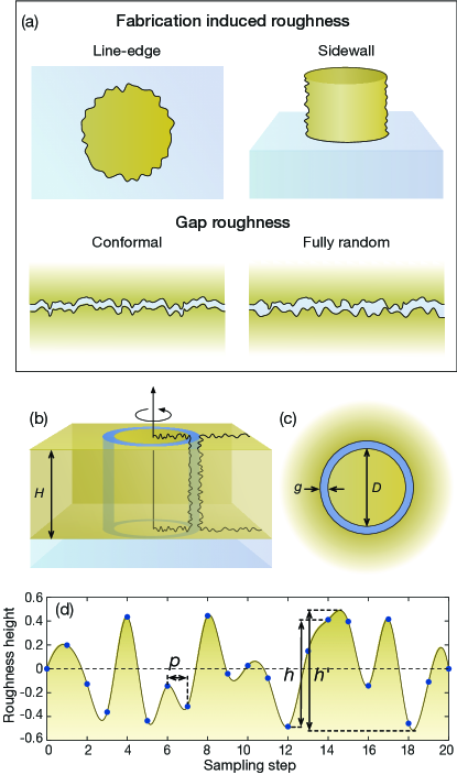
Fabrication of coaxial nanoapertures involves four steps 40: first, gold nanopillars are patterned via electron-beam lithography; the pillars are then coated by gap-filling insulator (Al2O3) using atomic layer deposition (ALD); the resulting structure is covered with gold by sputtering; finally, ion milling is used to planarize the top surface and expose the Al2O3-filled nanocoaxial apertures. The lithography step introduces two different kind of irregularities: a line-edge roughness (seen from the top) that prevents the apertures from being perfectly circular, and a sidewall roughness. Because of the nature of the ALD process, the gap is conformal to the sidewall irregularities. However, a fully random source for the gap roughness cannot be excluded, so that in general the gap is affected by some combination of both types of irregularities. For clarity we have summarized all of the kinds of roughnesses in Fig. 1a.
Numerically modeling random nanoscale surface roughness can be challenging for two reasons. On one hand, it requires extended computational resources, since for example one cannot use periodic conditions and would need to discretize much more finely the computational space in order to resolve the roughness details. On the other hand, it is not straightforward creating randomness along an arbitrary surface. In order to overcome these issues, we consider isolated structures, i.e. a single annular aperture in an infinitely extended metallic film, and we solve Maxwell’s equations using the so called 2.5D technique 42, 43. This technique consists in expanding all the fields in cylindrical harmonics by exploiting the axis symmetry of the geometry. In this way one needs to solve just few two-dimensional problems while still maintaining the three-dimensionality of the original one. The drawback of this approach is that roughness can be created only in the cross-sectional plane, that is, the structure will still be smooth along the azimuthal direction as shown in Fig. 1b-c. A more general implementation could be in principle obtained by employing more complex numerical schemes that allow curvilinear elements44, 45, 46. Such schemes, however, go beyond the scope of this work. In this letter, we neglect line-edge roughness and consider the apertures to be perfectly circular. Moreover, we analyze irregular structures with perfectly conformal gaps and fully random gap roughness separately.
Although roughness can be readily measured on planar thin films 47 using an atomic force microscope, it is not straightforward to do the same for sidewalls of gold pillars. However, because in both cases roughness has an analogous origin we assume a roughness amplitude of the same order. In order to describe surface roughness we use two parameters: the roughness maximum height, , and the sampling step or average period of the roughness, , as shown in Fig. 1d. Throughout the manuscript, we consider nm.
Our 2.5D approach greatly simplifies the creation of a randomly rough geometry. It is in fact possible to draw the geometry cross-section by randomly displacing each point of the curve by a distance , following steps of , where is the nominal maximum roughness height. The result is a set of points that are interpolated using a spline in order to smooth the curve and avoid numerical artifacts. Note that by using spline interpolation we may get displacements between the nominal and effective maximum height, that is . An example of the result of this process is depicted in Fig. 1d. We have implemented the 2.5D solver in a commercially available finite-element method software, Comsol Multiphysics. The geometry is created using a Matlab script in order to produce a set of points that are then interpolated directly in Comsol.
We consider coaxial nanoapertures drawn on an infinitely extended gold film of thickness nm, characterized by an internal diameter nm and a nominal gap varying from 2 to 10 nm, as depicted in Fig. 1b-c. The structure is excited by a plane wave impinging at normal incidence through an infinite sapphire substrate. The apertures are filled with Al2O3. The permittivity of sapphire is obtained using the Sellmeier’s formula with parameters as in Ref. 40, while the dispersive dielectric constant of Al2O3 is extracted from the experimental measurements 48. Gold local permittivity is approximated by a Drude formula with eV and eV. For completeness, we have also calculated the response of system when the electron pressure is taken into account, that is, when the metal response is nonlocal 27, 46, 49.This is taken into account adding a correction of the form to the Drude model 27, where is proportional to the Fermi velocity. Here we take m/s. In order to characterize the optical response of the systems, we compute the absorption efficiency as , where is the power dissipated in the entire structure, is the power dissipated by a continuous film (i.e. without aperture), is the input intensity and is the geometrical cross-section of the aperture. This definition removes all dependencies on the film extension.
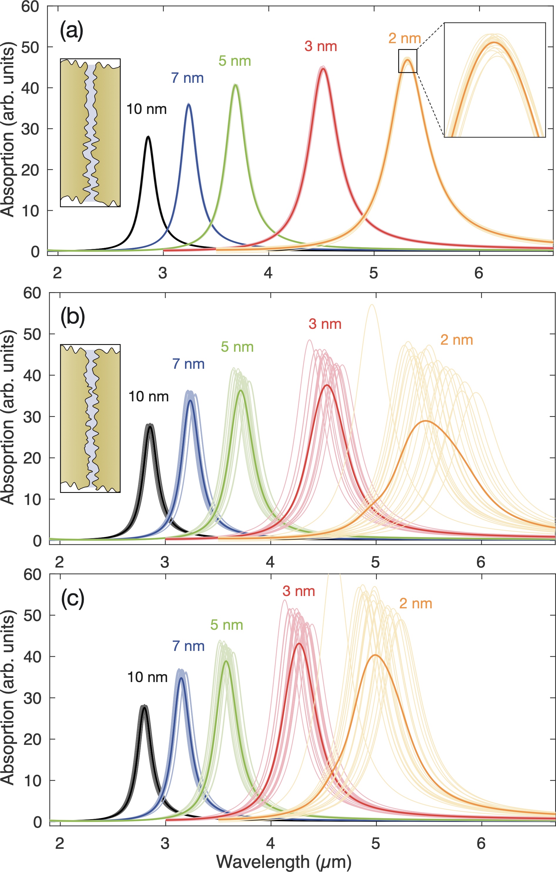
Using the techniques described above we have generated 20 different numerical samples for each nominal gap size, for both types of gap roughness, conformal with nm () and fully random with nm (). In Fig. 2, we show a set of absorption spectra around the zero--order mode resonance 40, 50, 46, as well as the mean curve obtained by averaging the results from all the random samples. As expected, the resonance of the system undergoes a shift towards longer wavelengths as the average gap size is reduced. It is interesting to note the difference between conformal (Fig. 2a) and random (Fig. 2b) gap roughness. While in the first case (Fig. 2a) the impact of roughness is minimal, producing small oscillations of the peak resonance even for the smallest gap, in the second case (Fig. 2b), the impact of roughness is substantial and variations of the peak resonance increase as the gap size shrinks. It is clear from these simulations that the effect of the roughness is to randomly shift (towards higher or lower frequencies) the resonance of the system. An analogous behavior can be observed for other resonances (i.e. the first order Fabry-Pérot mode resonance, not reported here). In Fig. 2c, we report calculations for the same numerical samples of Fig. 2b when the nonlocal response of gold free electrons is considered. As expected the average resonance results in an increasing blue-shift compared to the local case, as the gap is reduced. More interestingly however is the fact that for each nominal gap size the spectra are more tightly packed compared to the local case. This is especially visible for smaller gaps. The effect of the electron pressure is to spread the electron accumulation charge induced by an external field inward with respect to the metal surface. This can in some cases—for example when roughness produces sub-nanometer asperities—even mitigate the detrimental impact of surface roughness on the propagation length of surface plasmons 51. Analogously, in this case the effect of the electron pressure is to smooth out some roughness features so that the global effect is a reduced random oscillation of the peak resonance caused by the randomness of the roughness.
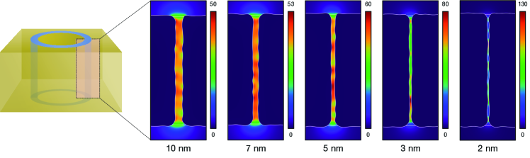
The impact of roughness on the near-field is shown in Fig. 3, where we show the electric field enhancement, , at resonance, propagating through the aperture obtained for a typical sample for each gap size. The resonance corresponds to an effective epsilon-near-zero mode, which is characterized by a constant phase, and hence norm, of the field along its propagation through the gap 50. For large gaps ( nm) this is still the case, while for smaller gaps ( nm) the randomness of the structure creates local hot spots where the field is strongly enhanced.
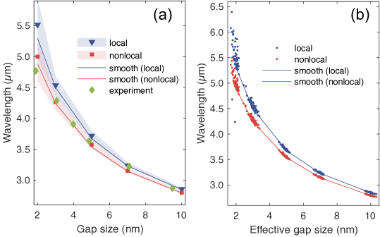
To understand the global impact of roughness on different gap sizes, in Fig. 4a we show the epsilon-near-zero mode resonance as a function of the nominal gap size . The shaded regions represent the maximum deviation introduced by the fully random roughness. As already seen in Fig. 2, the smaller the gap the larger the variance. The mean value (indicated by triangles and squares) is mostly unchanged with respect to the perfectly smooth structure for all gaps except the smallest. In this case, the averaged resonance results are slightly shifted toward longer wavelengths compared to the smooth structure. Fig. 4a shows more clearly that the impact of electron pressure on coaxial nanoapertures is to slightly reduce (with respect to local calculations) the shift caused by the reduction of the gap size. This is consistent with numerical results obtained for smooth structures 46. Together with our numerical data, we report in Fig. 4a the experimental data measured in Ref. 40. Note that the experimental data remain within the roughness deviation of the nonlocal calculations, and are clearly outside the span of local results.
It is interesting at this point to understand the nature of the shift induced by the gap roughness. In order to do so, we have evaluated the effective gap size corresponding to 3 sets of samples obtained for nm ( nm). The effective gap for each sample —one sample corresponds to a realization of random roughness for a given nominal gap and — is evaluated by numerically integrating the gap surface on a vertical cross-section, see Fig. 1b, and dividing it by the gold film thickness . The epsilon-near-zero mode resonance for each sample is plotted against the effective gap size in Fig. 4b, for both local and nonlocal cases. It is surprising how well the single samples follow the trajectory of the smooth structure. This clearly shows that the resonance shift due to roughness is mostly driven by the variation that the roughness induces in the effective gap. This effect is of course absent in the case of conformal roughness, where the effective gap always corresponds to the nominal gap.
In conclusion, we have analyzed the impact of nanoscale surface roughness on single coaxial nanoapertures characterized by gaps of few nanometers. Although our approach was limited to roughness on the cross-sectional plane of the systems, we are confident similar results will hold in the general case. It is very unlikely in fact that full three-dimensional surface roughness might lead to different conclusions. We have shown that while the impact of conformal gap roughness is negligible, fully random roughness might strongly affect the resonance shift of individual samples. Moreover, the roughness-induced perturbation on the peak resonance has a strong correlation with the effective gap size for each individual sample. A large number of samples then can average out the fluctuations due to fabrication imperfections and still provide a precise measure of the ideal system’s optical properties. Experimentally, this is naturally achieved by performing measurements on structure ensembles.
F.V.-C. and J.P. acknowledge support from the AFOSR Grant No. FA9550-15-1-0276 and FA9550-16-0214. D.Y. and S-H.O. acknowledge support from the National Science Foundation (NSF ECCS 1809723 and ECCS 1809240) and Sanford P. Bordeau Endowed Chair at the University of Minnesota. D.R.S. acknowledges funding from AFOSR (Grant No. FA9550-18-1-0187).
1 Notes
The authors declare no competing financial interest.
References
- Hill et al. 2010 Hill, R. T.; Mock, J. J.; Urzhumov, Y. A.; Sebba, D. S.; Oldenburg, S. J.; Chen, S.-Y.; Lazarides, A. A.; Chilkoti, A.; Smith, D. R. Leveraging nanoscale plasmonic modes to achieve reproducible enhancement of light. Nano Lett. 2010, 10, 4150–4154
- Moreau et al. 2012 Moreau, A.; Ciracì, C.; Mock, J. J.; Hill, R. T.; Wang, Q.; Wiley, B. J.; Chilkoti, A.; Smith, D. R. Controlled-reflectance surfaces with film-coupled colloidal nanoantennas. Nature 2012, 492, 86–89
- Duan et al. 2012 Duan, H.; Fernández-Domínguez, A. I.; Bosman, M.; Maier, S. A.; Yang, J. K. W. Nanoplasmonics: Classical down to the nanometer scale. Nano Lett. 2012, 12, 1683–1689
- Chen et al. 2013 Chen, X.; Park, H.-R.; Pelton, M.; Piao, X.; Lindquist, N. C.; Im, H.; Kim, Y. J.; Ahn, J. S.; Ahn, K. J.; Park, N.; Kim, D.-S.; Oh, S.-H. Atomic layer lithography of wafer-scale nanogap arrays for extreme confinement of electromagnetic waves. Nat. Commun. 2013, 4, 2361
- Stewart et al. 2017 Stewart, J. W.; Akselrod, G. M.; Smith, D. R.; Mikkelsen, M. H. Toward Multispectral Imaging with Colloidal Metasurface Pixels. Adv. Mater. 2017, 29, 1602971–6
- Chikkaraddy et al. 2016 Chikkaraddy, R.; de Nijs, B.; Benz, F.; Barrow, S. J.; Scherman, O. A.; Rosta, E.; Demetriadou, A.; Fox, P.; Hess, O.; Baumberg, J. J. Single-molecule strong coupling at room temperature in plasmonic nanocavities. Nature 2016, 535, 127–130
- Readman et al. 2019 Readman, C.; de Nijs, B.; Szabó, I.; Demetriadou, A.; Greenhalgh, R.; Durkan, C.; Rosta, E.; Scherman, O. A.; Baumberg, J. J. Anomalously Large Spectral Shifts near the Quantum Tunnelling Limit in Plasmonic Rulers with Subatomic Resolution. Nano Lett. 2019, 19, 2051–2058
- Halas et al. 2011 Halas, N. J.; Lal, S.; Chang, W.-S.; Link, S.; Nordlander, P. Plasmons in Strongly Coupled Metallic Nanostructures. Chem. Rev. 2011, 111, 3913–3961
- Fernández-Domínguez et al. 2012 Fernández-Domínguez, A. I.; Zhang, P.; Luo, Y.; Maier, S. A.; García-Vidal, F. J.; Pendry, J. B. Transformation-optics insight into nonlocal effects in separated nanowires. Phys. Rev. B 2012, 86, 241110
- Esteban et al. 2012 Esteban, R.; Borisov, A. G.; Nordlander, P.; Aizpurua, J. Bridging quantum and classical plasmonics with a quantum-corrected model. Nat. Comm. 2012, 3, 825
- Wiener et al. 2013 Wiener, A.; Fernández-Domínguez, A. I.; Pendry, J. B.; Horsfield, A. P.; Maier, S. A. Nonlocal propagation and tunnelling of surface plasmons in metallic hourglass waveguides. Opt. Express 2013, 21, 27509
- Barbry et al. 2015 Barbry, M.; Koval, P.; Marchesin, F.; Esteban, R.; Borisov, A. G.; Aizpurua, J.; Sánchez-Portal, D. Atomistic Near-Field Nanoplasmonics: Reaching Atomic-Scale Resolution in Nanooptics. Nano Lett. 2015, 15, 3410–3419
- Zhu et al. 2016 Zhu, W.; Esteban, R.; Borisov, A. G.; Baumberg, J. J.; Nordlander, P.; Lezec, H. J.; Aizpurua, J.; Crozier, K. B. Quantum mechanical effects in plasmonic structures with subnanometre gaps. Nat. Comm. 2016, 7, 11495
- Carnegie et al. 2018 Carnegie, C.; Griffiths, J.; de Nijs, B.; Readman, C.; Chikkaraddy, R.; Deacon, W. M.; Zhang, Y.; Szabó, I.; Rosta, E. R.; Aizpurua, J.; Baumberg, J. J. Room-Temperature Optical Picocavities below 1 nm3 Accessing Single-Atom Geometries. J. Phys. Chem. Lett. 2018, 9, 7146–7151
- Yang et al. 2019 Yang, F.; Wang, Y.-T.; Huidobro, P. A.; Pendry, J. B. Nonlocal effects in singular plasmonic metasurfaces. Phys. Rev. 2019, 99, 165423
- Baumberg et al. 2019 Baumberg, J. J.; Aizpurua, J.; Mikkelsen, M. H.; Smith, D. R. Extreme nanophotonics from ultrathin metallic gaps. Nat. Mater. 2019, 18, 668–678
- Wang et al. 2006 Wang, H.; Fu, K.; Drezek, R. A.; Halas, N. J. Light scattering from spherical plasmonic nanoantennas: effects of nanoscale roughness. Appl. Phys. B 2006, 84, 191–195
- Rodríguez-Fernández et al. 2009 Rodríguez-Fernández, J.; Funston, A. M.; Pérez-Juste, J.; Álvarez-Puebla, R. A.; Liz-Marzán, L. M.; Mulvaney, P. The effect of surface roughness on the plasmonic response of individual sub-micron gold spheres. Phys. Chem. Chem. Phys. 2009, 11, 5909–5914
- Trügler et al. 2011 Trügler, A.; Tinguely, J.-C.; Krenn, J. R.; Hohenau, A.; Hohenester, U. Influence of surface roughness on the optical properties of plasmonic nanoparticles. Phys. Rev. B 2011, 83, 916–4
- Huang et al. 2010 Huang, J.-S.; Callegari, V.; Geisler, P.; Brüning, C.; Kern, J.; Prangsma, J. C.; Wu, X.; Feichtner, T.; Ziegler, J.; Weinmann, P.; Kamp, M.; Forchel, A.; Biagioni, P.; Sennhauser, U.; Hecht, B. Atomically flat single-crystalline gold nanostructures for plasmonic nanocircuitry. Nat. Comm. 2010, 1, 150
- Park et al. 2012 Park, J. H.; Nagpal, P.; Oh, S.-H.; Norris, D. J. Improved dielectric functions in metallic films obtained via template stripping. Appl. Phys. Lett. 2012, 100, 081105
- Martin and Paulus 2002 Martin, O. J. F.; Paulus, M. Influence of metal roughness on the near-field generated by an aperture/apertureless probe. J. Micorsc. 2002, 205, 147–152
- Tinguely et al. 2011 Tinguely, J.-C.; Sow, I.; Leiner, C.; Grand, J.; Hohenau, A.; Felidj, N.; Aubard, J.; Krenn, J. R. Gold Nanoparticles for Plasmonic Biosensing: The Role of Metal Crystallinity and Nanoscale Roughness. BioNanoSci. 2011, 1, 128–135
- Lumdee et al. 2015 Lumdee, C.; Yun, B.; Kik, P. G. Effect of surface roughness on substrate-tuned gold nanoparticle gap plasmon resonances. Nanoscale 2015, 7, 4250–4255
- Ning et al. 2017 Ning, T.; Gao, S.; Huo, Y.; Jiang, S.; Yang, C.; Li, J.; Zhao, Y.; Man, B. Third-harmonic generation from gold nanowires of rough surface considering classical nonlocal effect. Opt. Express 2017, 25, 6372–11
- Ciracì et al. 2012 Ciracì, C.; Hill, R. T.; Mock, J. J.; Urzhumov, Y. A.; Fernandez-Dominguez, A. I.; Maier, S. A.; Pendry, J. B.; Chilkoti, A.; Smith, D. R. Probing the ultimate limits of plasmonic enhancement. Science 2012, 337, 1072–1074
- Raza et al. 2015 Raza, S.; Bozhevolnyi, S. I.; Wubs, M.; Mortensen, N. A. Nonlocal optical response in metallic nanostructures. J. Phys.: Condens. Mat. 2015, 27, 183204
- Doyle et al. 2017 Doyle, D.; Charipar, N.; Argyropoulos, C.; Trammell, S. A.; Nita, R.; Naciri, J.; Piqué, A.; Herzog, J. B.; Fontana, J. Tunable Subnanometer Gap Plasmonic Metasurfaces. ACS Photonics 2017, 5, 1012–1018
- Hajisalem et al. 2014 Hajisalem, G.; Min, Q.; Gelfand, R.; Gordon, R. Effect of surface roughness on self-assembled monolayer plasmonic ruler in nonlocal regime. Opt. Express 2014, 22, 9604
- Hajisalem et al. 2014 Hajisalem, G.; Nezami, M. S.; Gordon, R. Probing the quantum tunneling limit of plasmonic enhancement by third harmonic generation. Nano Lett. 2014, 14, 6651–6654
- Ciracì et al. 2014 Ciracì, C.; Chen, X.; Mock, J. J.; McGuire, F.; Liu, X.; Oh, S.-H.; Smith, D. R. Film-coupled nanoparticles by atomic layer deposition: Comparison with organic spacing layers. Appl. Phys. Lett. 2014, 104, 023109
- Kern et al. 2012 Kern, J.; Großmann, S.; Tarakina, N. V.; Häckel, T.; Emmerling, M.; Kamp, M.; Huang, J.-S.; Biagioni, P.; Prangsma, J. C.; Hecht, B. Atomic-scale confinement of resonant optical fields. Nano Lett. 2012, 12, 5504–5509
- Savage et al. 2012 Savage, K. J.; Hawkeye, M. M.; Esteban, R.; Borisov, A. G.; Aizpurua, J.; Baumberg, J. J. Revealing the quantum regime in tunnelling plasmonics. Nature 2012, 491, 574–577
- Scholl et al. 2013 Scholl, J. A.; García-Etxarri, A.; Koh, A. L.; Dionne, J. A. Observation of quantum tunneling between two plasmonic nanoparticles. Nano Lett. 2013, 13, 564–569
- Raza et al. 2013 Raza, S.; Stenger, N.; Stenger, N.; Kadkhodazadeh, S.; Kadkhodazadeh, S.; Fischer, S. V.; Fischer, S. V.; Kostesha, N.; Jauho, A.-P.; Burrows, A.; Wubs, M.; Mortensen, N. A. Blueshift of the surface plasmon resonance in silver nanoparticles studied with EELS. Nanophotonics 2013, 2, 131–138
- Cha et al. 2014 Cha, H.; Yoon, J. H.; Yoon, S. Probing Quantum Plasmon Coupling Using Gold Nanoparticle Dimers with Tunable Interparticle Distances Down to the Subnanometer Range. ACS Nano 2014, 8, 8554–8563
- Tan et al. 2014 Tan, S. F.; Wu, L.; Yang, J.; Bai, P.; Bosman, M.; 2014, Quantum plasmon resonances controlled by molecular tunnel junctions. Science 2014, 343, 1496–1499
- Zhu and Crozier 2014 Zhu, W.; Crozier, K. B. Quantum mechanical limit to plasmonic enhancement as observed by surface-enhanced Raman scattering. Nat. Commun. 2014, 5, 5228
- Campos et al. 2019 Campos, A.; Troc, N.; Cottancin, E.; Pellarin, M.; Weissker, H.-C.; Lermé, J.; Kociak, M.; Hillenkamp, M. Plasmonic quantum size effects in silver nanoparticles are dominated by interfaces and local environments. Nat. Physics 2019, 15, 275–280
- Yoo et al. 2019 Yoo, D.; Vidal-Codina, F.; Ciracì, C.; Nguyen, N.-C.; Smith, D. R.; Peraire, J.; Oh, S.-H. Modeling and observation of mid-infrared nonlocality in effective epsilon-near-zero ultranarrow coaxial apertures. Nat. Comm. 2019, 40, 4476
- Kretschmann et al. 1979 Kretschmann, E.; Ferrell, T. L.; Ashley, J. C. Splitting of the dispersion relation of surface plasmons on a rough surface. Phys. Rev. Lett. 1979, 42, 1312–1314
- Ciracì et al. 2013 Ciracì, C.; Smith, D. R.; Urzhumov, Y. A. Far-field analysis of axially symmetric three-dimensional directional cloaks. Opt. Express 2013, 21, 9397–9406
- Jurga et al. 2017 Jurga, R.; D’Agostino, S.; Della Sala, F.; Ciracì, C. Plasmonic Nonlocal Response Effects on Dipole Decay Dynamics in the Weak- and Strong-Coupling Regimes. J. Phys. Chem. C 2017, 121, 22361–22368
- Schmitt et al. 2018 Schmitt, N.; Scheid, C.; Viquerat, J.; Lanteri, S. Simulation of three-dimensional nanoscale light interaction with spatially dispersive metals using a high order curvilinear DGTD method. J. Comput. Phys. 2018, 373, 210–229
- Li et al. 2017 Li, L.; Lanteri, S.; Mortensen, N. A.; Wubs, M. A hybridizable discontinuous Galerkin method for solving nonlocal optical response models. Comput. Phys. Commun. 2017, 219, 99–107
- Vidal-Codina et al. 2018 Vidal-Codina, F.; Nguyen, N. C.; Oh, S. H.; Peraire, J. A hybridizable discontinuous Galerkin method for computing nonlocal electromagnetic effects in three-dimensional metallic nanostructures. J. Comput. Phys. 2018, 355, 548–565
- Nagpal et al. 2009 Nagpal, P.; Lindquist, N. C.; Oh, S. H.; Norris, D. J. Ultrasmooth Patterned Metals for Plasmonics and Metamaterials. Science 2009, 325, 594–597
- Kischkat et al. 2012 Kischkat, J.; Peters, S.; Gruska, B.; Semtsiv, M.; Chashnikova, M.; Klinkmüller, M.; Fedosenko, O.; MacHulik, S.; Aleksandrova, A.; Monastyrskyi, G.; Flores, Y.; Masselink, W. T. Mid-infrared optical properties of thin films of aluminum oxide, titanium dioxide, silicon dioxide, aluminum nitride, and silicon nitride. Appl. Optics 2012, 51, 6789–6798
- Shen et al. 2017 Shen, H.; Chen, L.; Ferrari, L.; Lin, M.-H.; Mortensen, N. A.; Gwo, S.; Liu, Z. Optical Observation of Plasmonic Nonlocal Effects in a 2D Superlattice of Ultrasmall Gold Nanoparticles. Nano Lett. 2017, 17, 2234–2239
- Yoo et al. 2016 Yoo, D.; Nguyen, N.-C.; Martín Moreno, L.; Mohr, D. A.; Carretero-Palacios, S.; Shaver, J.; Peraire, J.; Ebbesen, T. W.; Oh, S.-H. High-Throughput Fabrication of Resonant Metamaterials with Ultrasmall Coaxial Apertures via Atomic Layer Lithography. Nano Lett. 2016, 16, 2040–2046
- Wiener et al. 2012 Wiener, A.; Fernández-Domínguez, A. I.; Horsfield, A. P.; Pendry, J. B.; Maier, S. A. Nonlocal effects in the nanofocusing performance of plasmonic tips. Nano Lett. 2012, 12, 3308–3314
![[Uncaptioned image]](/html/2001.08953/assets/x4.png)