Projected sensitivity to sub-GeV dark matter of next-generation semiconductor detectors
Abstract
We compute the projected sensitivity to dark matter (DM) particles in the sub-GeV mass range of future direct detection experiments using germanium and silicon semiconductor targets. We perform this calculation within the dark photon model for DM-electron interactions using the likelihood ratio as a test statistic, Monte Carlo simulations, and background models that we extract from recent experimental data. We present our results in terms of DM-electron scattering cross section values required to reject the background only hypothesis in favour of the background plus DM signal hypothesis with a statistical significance, , corresponding to 3 or 5 standard deviations. We also test the stability of our conclusions under changes in the astrophysical parameters governing the local space and velocity distribution of DM in the Milky Way. In the best-case scenario, when a high-voltage germanium detector with an exposure of kg-year and a CCD silicon detector with an exposure of kg-year and a dark current rate of counts/pixel/day have simultaneously reported a DM signal, we find that the smallest cross section value compatible with () is about cm2 ( cm2) for contact interactions, and cm2 ( cm2) for long-range interactions. Our sensitivity study extends and refine previous works in terms of background models, statistical methods, and treatment of the underlying astrophysical uncertainties.
1 Introduction
The presence of Dark Matter (DM) in the Universe has firmly been established through increasingly accurate cosmological observations [1]. Evidence has been gathered in a wide range of physical scales, from sub-galactic scales to the largest scales we can probe in the Universe [2]. This includes data on the vertical motion of stars in the solar neighbourhood [3], the rotation curve of spiral galaxies [4], the velocity dispersion of galaxies in galaxy clusters [5], gravitational lensing events [6], the dynamics of colliding clusters [7], the large-scale cosmological structures [8] and anisotropies in the cosmic microwave background temperature [9]. While the evidence for DM is strong, it is entirely based on gravitational effects, directly or indirectly related to the gravitational pull that DM exerts on visible matter and light. As a result, we still do not know whether or not DM is made of particles which have so far escaped detection. One promising approach to answer this question is the so-called DM direct detection technique [10, 11].
Direct detection experiments search for DM-nucleus or -electron scattering events in low-background detectors located deep underground [12]. Next generation direct detection experiments searching for signals of DM-electron interactions with germanium and silicon semiconductor detectors of mass in the 0.1 - 1 kg range [13, 14, 15] are of special interest to this work. In these detectors, the energy deposited in a DM-electron scattering event can cause an observable electronic transition from the valence to the conduction band of the semiconductor target. For kinematical reasons, this detection principle can outperform methods based on nuclear recoils in the search for DM particles in the 1 MeV to 1 GeV mass range [16]. Sub-GeV DM can also be searched for with, e.g. dual-phase argon [17] and xenon [18, 19, 20] targets, graphene [21, 22], 3D Dirac materials [23, 24, 25], polar crystals [26], scintillators [27, 28] and superconductors [29, 30, 31]. For a comparison of the performance of different materials in the search for sub-GeV DM, see [32].
For the purposes of this paper, we divide detectors based on germanium and silicon semiconductor crystals into two categories: 1) “high-voltage” (HV) detectors; and 2) “charge-coupled device” (CCD) detectors. Detectors operating in HV mode have the capability to amplify the small charge produced by DM scattering in target crystals into a large phonon signal by applying a bias of about 100 V across the detector and exploiting the so-called Neganov-Trofimov-Luke effect [33]. The SuperCDMS experiment demonstrated that this approach allows to achieve sensitivity to single-charge production [34]. Similarly, CCD sensors can achieve single-charge sensitivity by measuring the charge collected by single pixels in the CCD device exploiting ultra-low readout noise techniques, as in “Skipper” CCDs [35]. Currently operating experiments belonging to the first category include the HV mode run of the silicon SuperCDMS experiment, which delivered data corresponding to an exposure of 0.49 gram-days [34]. The null result reported by this search has been used to set a 90% C.L exclusion limit of cm2 on the cross section for DM-electron scattering for DM-particle masses around 1 MeV. For the future, the SuperCDMS collaboration plans to operate in the HV mode larger germanium and silicon detectors, reaching an exposure of about 50 and 10 kg-year, respectively [13]. Operating DM direct detection experiments belonging to the second category include the DAMIC and SENSEI experiments, both using CCD silicon sensors. For example, the null result of the SENSEI experiment has been used to set 90% C.L exclusion limits on the DM-electron scattering cross section for DM particle masses in the 0.5 - 100 MeV range, with a minimum excluded cross section of about cm2 for a DM mass of about 10 MeV (and short-range interactions) [35]. For the future, the SENSEI and DAMIC collaborations aim at building CCD silicon detectors of 0.1 kg and 1 kg target mass, respectively [14, 15].
Predictions for the rate of DM-induced electronic transitions in semiconductor crystals depend on a number of theoretical and experimental inputs [16, 36, 37, 38, 39, 14, 34, 35, 15, 40]. Firstly, they depend on the assumed DM-electron interaction model, e.g. on whether the interaction is long- or short-range and on its Lorentz structure [40]. Secondly, they depend on the semiconductor band structure, and in particular on the initial and final state electron energy and wave functions [38]. They also depend on astrophysical inputs, such as the local DM density and velocity distribution, as well as on detector characteristics such as energy threshold, efficiency, and energy deposition to number of produced electron-hole pairs conversion, just to name a few.
Motivated by the recent experimental results reviewed above and by the improved understanding of the experimental backgrounds that these results have produced, this article aims at assessing the sensitivity to DM particles in the sub-GeV mass range of future direct detection experiments using germanium and silicon semiconductor crystals as target materials. We address this problem focusing on the so-called “dark photon” model [41, 16] as a framework to describe the interactions of DM in semiconductor crystals. We compute the projected sensitivities of future germanium and silicon detectors by comparing the null, i.e. background-only hypothesis to the alternative, i.e. background plus signal hypothesis using the likelihood ratio as a test statistic [42]. Doing so, we provide a detailed description of the background models used in our analysis. We present our results in terms of the DM-electron scattering cross section required to reject the null hypothesis in favour of the alternative one with a statistical significance corresponding to 3 or 5 standard deviations. We compute the significance for DM particle discovery using asymptotic formulae for the probability density function of the likelihood ratio [42], after explicitly validating them by means of Monte Carlo simulations. We also test the stability of our results under variations in the underlying astrophysical inputs. Our sensitivity study extends previous works, e.g. [38], by: 1) adopting a refined experimental background model 2) computing the projected sensitivity by using the likelihood ratio method; and 3) exploring the dependence of our results on the DM space and velocity distribution.
This paper is organised as follows. In Sec. 2, we review the theory of DM-electron scattering in silicon and germanium semiconductor crystals, while in Sec. 3 we describe the efficiency, energy threshold and experimental backgrounds assumed when modelling future HV germanium and silicon detectors, as well as future silicon CCD detectors. We present our methodology and projected sensitivities to sub-GeV DM particles in Sec. 4 and conclude in Sec. 5.
2 Dark matter scattering in semiconductor crystals
In this section, we review the theory of DM-electron scattering in semiconductor crystals. We start by presenting a general expression for the rate of DM-induced electronic transitions in condensed matter systems (Sec. 2.1). We then specialise this expression to the case of electronic transitions from the valence to the conduction band of germanium and silicon semiconductors (Sec. 2.2). As we will see, the transition rate found in Sec. 2.2 depends on an integral over DM particle velocities (Sec. 2.3) and on the amplitude for DM scattering by free electrons (Sec. 2.4).
2.1 Dark matter-induced electronic transitions
The rate of DM-induced transitions from an initial electron state to a final electron state is [40]
| (2.1) |
where is the DM particle mass, while and are the local DM number density and velocity distribution, respectively. If not otherwise specified, we set the local DM mass density to GeV/cm3 [43]. In all applications, for the local DM velocity distribution we assume [44]
| (2.2) |
that is, a truncated Maxwell-Boltzmann distribution boosted to the detector rest frame. Here implies that is unit-normalised. In Sec. 4, we present our results by varying most probable speed , detector’s velocity and galactic escape velocity within their experimental uncertainties (see Sec. 4.3 for further details). The squared electron transition amplitude, , depends on the initial and final state electron wave functions, and , respectively, and on the amplitude for DM scattering by free electrons, . Without any further restriction on the amplitude , it can be written as [40]
| (2.3) |
where a bar denotes an average (sum) over initial (final) spin states. Here, , with and initial and final DM particle momenta, respectively, is the momentum transfer and we introduced
| (2.4) |
where is the incoming DM particle velocity, the electron mass, and the reduced DM-electron mass. If the DM-electron scattering were elastic, would apply, justifying the notation. The initial and final state energies in Eq. (2.1) are defined as follows,
| (2.5) | ||||
| (2.6) |
where we denote the electron initial and final energy by and , and their difference by .
In the case of the “dark photon” model for DM-electron interactions (introduced below in Sec. 2.4), the free electron scattering amplitude only depends on , , and Eq. (2.1) simplifies to [40]
| (2.7) |
where is a scalar atomic form factor measuring the initial and final state wave function overlap 111As shown in [40], vectorial atomic form factors might also arise within a general treatment of DM-electron interactions.,
| (2.8) |
2.2 Crystal form factors
The above expressions refer to generic electronic transitions. We now specialise them to the case of transitions from a valence to the conduction band in a semiconductor crystal. In the case of crystals, electron states are labelled by a band index “” and a wavevector “” in the first Brillouin zone (BZ). In Bloch form, the associated wave functions can be expressed as [38]
| (2.9) |
where is the volume of the crystal, i.e. and , while is the reciprocal lattice vector. For the wave functions to be unit-normalised, the coefficients must fulfil
| (2.10) |
With these definitions, we can now interpret the transition rate in Eq. (2.1) as the transition rate, , from the valence level to the conduction level . Summing over all final state energy levels, and all filled initial state energy levels (while taking into account the initial state electron spin degeneracy), the resulting transition rate, , reads as follows [38]
| (2.11) |
where the deposited energy is defined as , the free electron scattering amplitude, , is assumed to be a function of only, as in the case of the dark photon model, and . Here is the volume of individual cells and is the number of cells in the crystal, where GeV for germanium and GeV for silicon [38], while is the detector target mass. The velocity integral in Eq. (2.1) is now reabsorbed in the definition of the function (given below in Sec. 2.3), while the crystal form factor is defined as [38]
| (2.12) |
where
| (2.13) |
and is the fine structure constant. In the numerical applications, we use germanium and silicon crystal form factors found in [38]. Following [38], we set eV for germanium and eV for silicon. Finally, we rewrite Eq. (2.2) in differential form, obtaining the differential rate of electronic transitions in germanium and silicon crystals,
| (2.14) |
In order to compare Eq. (2.14) with observations, one has to convert into a number of electron-hole pairs produced in a DM-electron scattering event, . The two quantities can be related as follows [38]
| (2.15) |
where is the floor function. The observed band-gap, , and mean energy per electron-hole pair, , are eV and eV for germanium, while eV and eV for silicon.
2.3 Kinematics
The function in Eq. (2.2) depends on the velocity distribution via a three-dimensional integral,
| (2.16) |
where , and is the minimum velocity required to induce a transition between two electronic states separated by the energy gap when the momentum transferred in the process is ,
| (2.17) |
The function in Eq. (2.16) arises from the integration over the momentum transfer in Eq. (2.1). The minimum velocity can also be derived from energy conservation, which implies
| (2.18) |
Maximising Eq. (2.18) with respect to the momentum transfer for a given energy gap gives back Eq. (2.17). For the velocity distribution in Eq. (2.2) (and for depending on only), the velocity integral in Eq. (2.14) can be evaluated analytically. For the result of this integration, see e.g. [44].
2.4 Dark matter-electron interaction model
In order to evaluate Eq. (2.2), we need to specify a model for DM-electron interactions from which to calculate . In this analysis, we focus on the so-called dark photon model [41, 16], which arises as an extension of the Standard Model (SM) of particle physics. In the dark photon model, the SM is extended by one DM candidate and one additional gauge group under which only the DM particle candidate is charged. The associated gauge boson, here denoted by , is the dark photon. Radiative corrections are generically expected to generate a kinetic mixing term between dark and ordinary photon, i.e. where () is the photon (dark photon) field strength tensor and is a dimensionless mixing parameter. This kinetic mixing acts as a portal between the DM and SM sectors. After a field redefinition which diagonalises the photon and dark photon kinetic terms, and assuming that the DM candidate is a Dirac fermion, the dark photon model can be formulated in terms of the following Lagrangian [41, 16]
| (2.19) |
where is the gauge coupling associated with the additional group, and are the dark photon and DM particle mass, respectively, while and are four-component Dirac spinors for the DM particle and the SM fermions, respectively. In the second line of Eq. (2.19), we denote by () the electric charge (mass) of the SM fermion. For the purposes of this analysis, we do not need to specify a mechanism for the spontaneous breaking of the additional gauge group and the generation of the dark photon and DM particle mass. Within the dark photon model the squared modulus of the amplitude for DM-electron scattering can be written as follows [38]
| (2.20) |
where is the reduced DM-electron mass, is a reference scattering cross section setting the strength of DM-electron interactions and is the “DM form factor” which encodes the -dependence of the amplitude. It reads for (short-range or contact interaction) and for (long-range interaction), where we set the reference momentum to the value , the typical momentum transfer in DM-induced electronic transitions.
3 Detector models
In this section we specify the experimental inputs we use and the assumptions we make to compute the statistical significance for DM discovery at direct detection experiments using germanium and silicon semiconductor crystals as target materials. We consider two classes of detectors separately: germanium and silicon HV detectors, as in future runs of the SuperCDMS experiment, and silicon CCDs, as in future runs of the DAMIC and SENSEI experiments.
3.1 High voltage Si/Ge detectors
We refer to HV detectors as experimental devices resembling the SuperCDMS experiment in the operating mode described in the recent analysis [34]. In this configuration, SuperCDMS exploits a 0.93 g high-purity silicon crystal instrumented on one side with transition-edge sensors and on the other side with an electrode made of an aluminum-amorphous silicon bilayer. This device can achieve single-charge resolution by exploiting the Neganov-Trofimov-Luke effect [33]. It consists in the emission of phonons generated by electron-hole pairs drifting across a bias of 140 V (the high voltage defining this operating mode). This effect can amplify the small charge signal associated with DM scattering in a HV detector into a large phonon signal.
In this work, we investigate the sensitivity of next generation HV detectors, taking the expected reach of SuperCDMS as a guideline [13]. Doing so, we focus on germanium and silicon targets separately, in that different exposures are planned for the two targets. More specifically, in the case of germanium HV detectors, we assume an exposure of 50 kg-year. For HV detectors using silicon targets, we assume an exposure of 10 kg-year (see Tab. 4 in [13] for further details).
Another important experimental input to our analysis is the detection efficiency of HV detectors. In general, only a fraction of DM-induced electronic transitions is expected to be successfully recorded by detectors used in DM direct detection experiments. The fraction of events that are successfully detected is called the detection efficiency. For both silicon and germanium HV detectors, we assume an energy-independent (i.e. -independent) detection efficiency of 90%, which is expected to be a fairly good approximation for between 1 and 8 [34]. When computing the expected number of DM signal events in a given -bin, we then multiply Eq. (2.14) by a detection efficiency factor for both germanium and silicon HV detectors. Here, “” is an index labelling the bin (see Sec. 4 for further details about event binning).
We now describe the experimental background model used for HV detectors in our sensitivity study. As demonstrated recently [34], charge leakage is the dominant background source in the search for DM-electron scattering events with HV detectors for values of Q less than 3. Indeed, large electric fields used in HV detectors can ionise impurities within the experimental apparatus causing charge carriers to tunnel into the crystal, producing a background event. We model the event spectrum associated with this experimental background by interpreting the events measured in [34] (orange line in Fig. 3) as due to charge leakage, as the authors suggest. For larger values of , ’s and ’s from the decay of radioactive isotopes originating from the experimental apparatus are also important [13]. In our sensitivity study, we model the Compton scattering of -rays from the decay of heavy radioactive isotopes as described in [45]. For the deposited energy spectrum induced by Compton scattering events from radiogenic ’s, we assume a constant function of , i.e. const., in the case of silicon HV detectors, and the following combination of error functions for germanium HV detectors [45]
| (3.1) |
where is a normalisation constant. In principle, Eq. (3.1) receives contributions from the , , , and shells of germanium. In the energy range of interest, however, only the germanium shell contribution with input parameters MeV-1, keV, eV [45] needs to be considered. Both for germanium and silicon, we conservatively normalise such that when integrated over the 0 - 50 eV range it gives 0.1 counts kg-1day-1 [13].
Finally, we assume that next generation HV germanium and silicon detectors will achieve single-charge resolution, which implies a sensitivity to energy depositions as low as the crystal’s band-gap, i.e. , where is the experimental threshold, i.e. the minimum number of detectable electron-hole pairs.
3.2 CCD detectors
For CCD detectors, DAMIC and SENSEI are our reference experiments. Both experiments exploit silicon semiconductor crystals as a target and already reported results from the run of prototype detectors [14, 15, 35]. For example, SENSEI recently reported data collected by using one silicon Skipper-CCD with a total active mass (before masking) of 0.0947 gram and consisting of pixels [35]. In a CCD, DM-electron scattering events can cause electronic transitions from the valence band to the conduction band of crystals in the device’s pixels. The excited electron subsequently creates additional electron-hole pairs for each 3.6 eV of excitation energy above the band gap which are then moved pixel-by-pixel to one of the CCD corners for the read-out.
Exploring the sensitivity to sub-GeV DM of CCD detectors, we focus on two benchmark values for the experimental exposure. These are: 1) 100 g-year, which is the exposure SENSEI aims at [14]; and 2) 1 kg-year, as expected for the next version of the DAMIC experiment, DAMIC-M [15]. As far as the detection efficiency of CCD detectors is concerned, we use the values reported in Tab. I of [35] in the “DM in single pixel” line. These values are: , , , , for the , , , , and bins, respectively. We set , for larger values of (). Consequently, when computing the expected number of DM signal events in the bin, we multiply Eq. (2.14) by .
“Dark current” events are expected to be the dominant experimental background source for next generation CCD detectors [35]. These events are evenly distributed across CCDs and are due to thermal fluctuations that excite electrons from the valence to the conduction band in crystals. As in Tab. 1 of [38], we assume that the number, , of dark current events generating at least electron-hole pairs in a crystal can be estimated in terms of Poisson probabilities ,
| (3.2) |
where is the number of CCDs in the detector, is the number of pixels in a CCD, is the time of data taking in hours and is the dark current rate in counts/pixel/hr. The number of these background events in the bin is then given by . As anticipated, we consider two benchmark cases: 1) , hr, corresponding to an exposure of 100 g-year, assuming that the mass of a single CCD is 2.5 g; and 2) , hr, corresponding to an exposure of 1 kg-year, again with 2.5 g. In each of the two scenarios above, we present our results for two extreme values of the dark current rate, namely counts/pixel/day and counts/pixel/day.
Similarly to the case of HV silicon detectors, for the deposited energy spectrum induced by Compton scattering events from radiogenic ’s, , we assume a constant function of . Conservatively, we normalise to 0.1 counts kg-1day-1 over the energy range 0 - 50 eV [13].
Background events due to voltage variations in the amplifiers used during read-out are assumed to be negligible, as they can be vetoed by means of a periodic read-out [35]. The measured rate at SENSEI for this class of background events is of the order of events/pixel/day and we assume that comparable rates will be achieved at next generation silicon CCD detectors.
Also in the case of silicon CCD detectors, we assume single-charge resolution, which implies .
4 Projected sensitivity
In Sec. 4.1, we introduce the statistical method used to compute the significance for a DM particle discovery at future germanium and silicon detectors. We present our results in Sec. 4.2, and investigate their stability under variations in the underlying astrophysical parameters in Sec. 4.3.
4.1 Methodology
We compute the significance for DM particle discovery at a given experiment, , using the likelihood ratio [42],
| (4.1) |
as a test statistic. In Eq. (4.1), is the likelihood function, the value of that maximises and ) a dataset. Here, is the observed number of electronic transitions in the -th -bin and the total number of bins in the variable is assumed to be . Notice that the larger , the worse fits the data and that for , takes its minimum value, i.e. zero. By repeatedly simulating under the null hypothesis, i.e. (for given , , , and ), we obtain a probability density function for denoted here by . Similarly, by repeatedly simulating under the alternative hypothesis, i.e. (for given , , , and ), we obtain , i.e. the probability density function of under the alternative hypothesis. The significance is then given by
| (4.2) |
where is the cumulative distribution function of a Gaussian probability density of mean 0 and variance 1, while
| (4.3) |
and is the median of . Notice that the significance given in Eq. (4.2) depends on as well as on the assumed values for , , , and . While both and can in principle be obtained via Monte Carlo simulations, asymptotically (i.e. in the large sample limit) is expected to obey a “half chi-square distribution” for one degree of freedom, [42]. For a few benchmark values of , , , and , we verified that is very well approximate by by comparing the latter with the distribution of found from 10 million Monte Carlo simulations of . Specifically, we find that the relative difference between the cumulative distribution functions of (the Monte Carlo generated) and is of the order of around . In order to speed up our numerical calculations, we therefore assume that the probability density function can be approximated by . At the same time, we compute the probability density function and from Monte Carlo simulations of . For the likelihood, we assume
| (4.4) |
where
| (4.5) |
while is the experimental exposure and, finally, is the total number of expected background events in the bin. In order to evaluate Eq. (4.5), we compute from Eq. (2.15). We introduced our assumptions for , and in Sec. 3 focusing on CCD and HV detectors separately. When computing the joint significance for DM discovery at two experiments and , we repeat the above procedure now with a likelihood function given by , where and are the likelihood functions for the experiments and , respectively.
4.2 Numerical results
We now present the results of our sensitivity study for future DM experiments based on germanium and silicon semiconductor detectors. We focus on the HV and CCD operating modes described in Sec. 3 and the dark photon model reviewed in Sec. 2. We present our results in terms of DM-electron scattering cross section, , required to reject the null, i.e. background only hypothesis with a statistical significance corresponding to 3 or 5 standard deviations as a function of the DM particle mass, and for benchmark values of , , and . We investigate the dependence of our results on the local DM density and escape velocity, most probable DM speed and detector speed in the galactic rest frame in the next subsection.
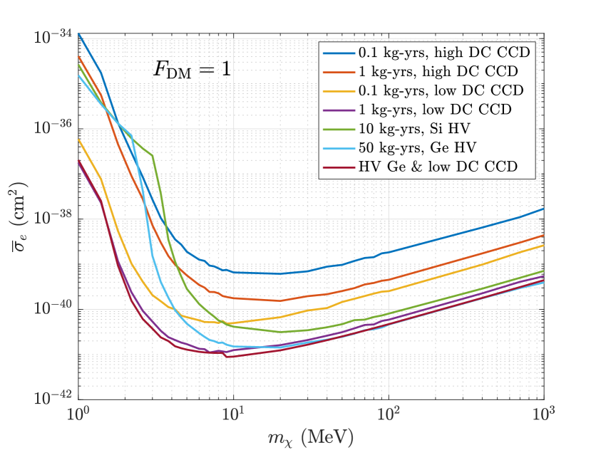
Fig. 1 shows the smallest cross section value, , required to reject the background only hypothesis with a statistical significance of at least 3 standard deviations when the DM particle mass varies in the 1 MeV - 1 GeV range. We obtain such contours using the likelihood ratio method described in Sec. 4.1. Results are presented for GeV cm-3, km s-1, km s-1 and km s-1. The left panel corresponds to the case , whereas in the right panel we assume . In both panels, lines with different colours correspond to distinct detectors, background assumptions or exposures. Specifically, we consider seven different experimental setups:
-
1.
CCD silicon detector operating with an exposure of kg-year and a high dark current rate of counts/pixel/day,
-
2.
CCD silicon detector operating with an exposure of kg-year and a high dark current rate of counts/pixel/day,
-
3.
CCD silicon detector operating with an exposure of kg-year and a low dark current rate of counts/pixel/day,
-
4.
CCD silicon detector operating with an exposure of kg-year and a low dark current rate of counts/pixel/day,
-
5.
HV silicon detector operating with an exposure of kg-year,
-
6.
HV germanium detector operating with an exposure of kg-year, and finally
-
7.
the case in which two distinct experiments have simultaneously reported data, namely a HV germanium detector with kg-year and a CCD silicon detector with kg-year and counts/pixel/day (i.e. the best-case scenario).
For larger than about 10 MeV, HV detectors are more sensitive to DM than CCD detectors operating in the first three modes described above. In the same mass range, however, the projected sensitivity of CCD silicon detectors operating with an exposure of kg-year and a low dark current rate of counts/pixel/day is comparable with the one of a HV germanium detector operating with an exposure of kg-year. Below MeV, HV detectors rapidly lose sensitivity because of the large number and the energy spectrum of charge leakage background events assumed for HV experiments in this study (see Sec. 3). In this second mass range, CCD silicon detectors are found to be more sensitive to DM than germanium and silicon HV detectors (at least for as low as 2-3 MeV). Overall, the projected sensitivity of CCD silicon detectors operating with an exposure of kg-year and a low dark current rate of counts/pixel/day is high (i.e. the cross section corresponding to is comparably small) over the whole range of DM particle masses considered here. This is especially true when , as illustrated in the right panel of Fig. 1. Finally, the contour that we find when a HV germanium detector with kg-year and a CCD silicon detector with kg-year and counts/pixel/day have simultaneously reported a DM signal is comparable with the contour we obtain for a CCD silicon detector with kg-year and (for both choices of ).
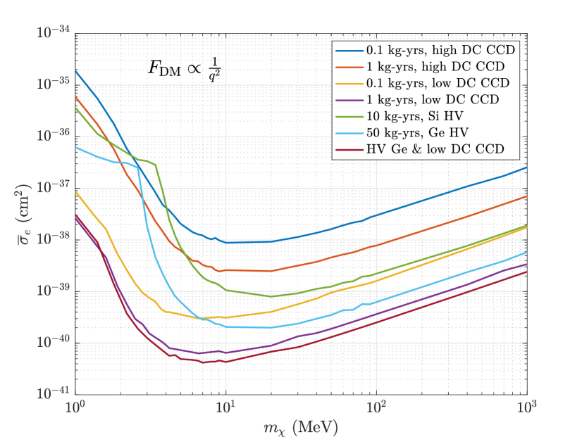
Similarly, Fig. 2 shows the smallest cross section value required to exclude the background only hypothesis with a statistical significance corresponding to at least 5 standard deviations. We obtain such contours in the (, ) plane for GeV cm-3, km s-1, km s-1 and km s-1. Compared to the case, the required cross section values are larger at each DM particle mass, but, as expected, above and below MeV the relative sensitivity of HV and CCD detectors is qualitatively unchanged.
4.3 Astrophysical uncertainties
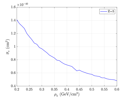
We conclude this section by investigating the stability of our conclusions under variations of the astrophysical parameters , , and governing the local space and velocity distribution of DM particles. We start by focusing on the local DM density, , upon which the rate of DM-induced electron transitions in semiconductor crystals, Eq. (2.14), linearly depends.
Fig. 3 shows the value of the DM-electron scattering cross section, , required to reject the null hypothesis with a statistical significance corresponding to as a function of the local DM density for a HV germanium detector with kg-year. Here, we assume and set MeV, km s-1, km s-1 and km s-1. As expected, we find that the value of solving is inversely proportional to .
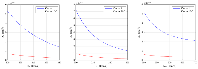
Similarly, Fig. 4 shows the value of required to reject the null hypothesis with a statistical significance of as a function of the detector speed in the galactic rest frame (left panel) of the most probable DM speed (central panel) and of the local escape velocity (right panel) for a CCD silicon detector with kg-year and counts/pixel/day. In all panels, we separately consider both (blue lines) and (red lines). Finally, we assume MeV and set to GeV cm-3. In all panels in Fig. 4, we find that the value of solving varies by a factor of a few over the range of astrophysical parameters considered here. As expected, we also find that astrophysical uncertainties have a smaller impact on our results for larger values of the DM particle mass. Notice also that in this analysis we treated and as independent parameters. This approach can account for the outcome of hydrodynamical simulations [46] and generalises the so-called Standard Halo Model, where the most probable speed, , is set to the speed of the local standard of rest [47].
5 Conclusions
We computed the sensitivity to DM particles in the sub-GeV mass range of future direct detection experiments using germanium and silicon semiconductor detectors. We addressed this problem within the dark photon model for DM-electron interactions in semiconductor crystals and computed the projected sensitivities of future germanium and silicon detectors by using the likelihood ratio as a test statistic and Monte Carlo simulations. We placed special emphasis on describing the background models used in our analysis and presented our results in terms of DM-electron scattering cross section values required to reject the background only hypothesis in favour of the background plus signal hypothesis with a statistical significance corresponding to 3 or 5 standard deviations. We also tested the stability of our results under variations in the astrophysical parameters that govern the space and velocity distribution of DM in our galaxy. Our sensitivity study extended previous works in terms of background models, statistical methods used to compute the projected sensitivities, and treatment of the underlying astrophysical uncertainties. This work is motivated by the recent experimental progress, and by the improved understanding of the experimental backgrounds that this progress produced.
For larger than about 10 MeV, HV detectors are more sensitive to DM than CCD detectors, with the exception of CCD silicon detectors operating with an exposure of kg-year and a low dark current rate of counts/pixel/day, which exhibit a sensitivity comparable with the one of a HV germanium detector operating with an exposure of kg-year. Below MeV, we find that CCD silicon detectors are more sensitive to DM than germanium and silicon HV detectors, at least for as low as 2-3 MeV. In the best-case scenario, when a HV germanium detector with kg-year and a CCD silicon detector with kg-year and counts/pixel/day have simultaneously reported a DM signal, we find that the smallest cross section value compatible with () is about cm2 ( cm2) for , and cm2 ( cm2) for .
Acknowledgments
We would like to thank Noah A. Kurinsky and Belina von Krosigk for useful insights into the backgrounds of SuperCDMS. During this work, RC and TE were supported by the Knut and Alice Wallenberg Foundation (PI, Jan Conrad). RC also acknowledges support from an individual research grant from the Swedish Research Council, dnr. 2018-05029. The research presented in this article made use of the computer programmes and packages WebPlotDigitizer [48], Wolfram Mathematica [49], Matlab [50] and QEdark [38].
References
- [1] G. Bertone and D. Hooper, History of dark matter, Rev. Mod. Phys. 90 (2018) 045002 [1605.04909].
- [2] G. Bertone, D. Hooper and J. Silk, Particle dark matter: Evidence, candidates and constraints, Phys. Rept. 405 (2005) 279 [hep-ph/0404175].
- [3] K. Kuijken and G. Gilmore, The Mass Distribution in the Galactic Disc - Part Two - Determination of the Surface Mass Density of the Galactic Disc Near the Sun, Mon. Not. Roy. Astron. Soc. 239 (1989) 605.
- [4] V. C. Rubin and W. K. Ford, Jr., Rotation of the Andromeda Nebula from a Spectroscopic Survey of Emission Regions, Astrophys. J. 159 (1970) 379.
- [5] Z. F., Die Rotverschiebung von extragalaktischen Nebeln, Phys. Acta 6 (1933) 110.
- [6] N. Kaiser and G. Squires, Mapping the dark matter with weak gravitational lensing, Astrophys. J. 404 (1993) 441.
- [7] D. Clowe, M. Bradac, A. H. Gonzalez, M. Markevitch, S. W. Randall, C. Jones et al., A direct empirical proof of the existence of dark matter, Astrophys. J. 648 (2006) L109 [astro-ph/0608407].
- [8] G. R. Blumenthal, S. M. Faber, J. R. Primack and M. J. Rees, Formation of Galaxies and Large Scale Structure with Cold Dark Matter, Nature 311 (1984) 517.
- [9] Planck collaboration, P. A. R. Ade et al., Planck 2015 results. XIII. Cosmological parameters, Astron. Astrophys. 594 (2016) A13 [1502.01589].
- [10] A. Drukier and L. Stodolsky, Principles and Applications of a Neutral Current Detector for Neutrino Physics and Astronomy, Phys. Rev. D30 (1984) 2295.
- [11] M. W. Goodman and E. Witten, Detectability of Certain Dark Matter Candidates, Phys. Rev. D31 (1985) 3059.
- [12] T. Marrodán Undagoitia and L. Rauch, Dark matter direct-detection experiments, J. Phys. G43 (2016) 013001 [1509.08767].
- [13] SuperCDMS collaboration, R. Agnese et al., Projected Sensitivity of the SuperCDMS SNOLAB experiment, Phys. Rev. D95 (2017) 082002 [1610.00006].
- [14] SENSEI collaboration, M. Crisler, R. Essig, J. Estrada, G. Fernandez, J. Tiffenberg, M. Sofo Haro et al., SENSEI: First Direct-Detection Constraints on sub-GeV Dark Matter from a Surface Run, Phys. Rev. Lett. 121 (2018) 061803 [1804.00088].
- [15] DAMIC collaboration, A. Aguilar-Arevalo et al., Constraints on Light Dark Matter Particles Interacting with Electrons from DAMIC at SNOLAB, Phys. Rev. Lett. 123 (2019) 181802 [1907.12628].
- [16] R. Essig, J. Mardon and T. Volansky, Direct Detection of Sub-GeV Dark Matter, Phys. Rev. D85 (2012) 076007 [1108.5383].
- [17] DarkSide collaboration, P. Agnes et al., Constraints on Sub-GeV Dark Matter-Electron Scattering from the DarkSide-50 Experiment, Phys. Rev. Lett. 121 (2018) 111303 [1802.06998].
- [18] R. Essig, A. Manalaysay, J. Mardon, P. Sorensen and T. Volansky, First Direct Detection Limits on sub-GeV Dark Matter from XENON10, Phys. Rev. Lett. 109 (2012) 021301 [1206.2644].
- [19] R. Essig, T. Volansky and T.-T. Yu, New Constraints and Prospects for sub-GeV Dark Matter Scattering off Electrons in Xenon, Phys. Rev. D96 (2017) 043017 [1703.00910].
- [20] XENON collaboration, E. Aprile et al., Light Dark Matter Search with Ionization Signals in XENON1T, Phys. Rev. Lett. 123 (2019) 251801 [1907.11485].
- [21] Y. Hochberg, Y. Kahn, M. Lisanti, C. G. Tully and K. M. Zurek, Directional detection of dark matter with two-dimensional targets, Phys. Lett. B772 (2017) 239 [1606.08849].
- [22] R. M. Geilhufe, B. Olsthoorn, A. Ferella, T. Koski, F. Kahlhoefer, J. Conrad et al., Materials Informatics for Dark Matter Detection, 1806.06040.
- [23] Y. Hochberg, Y. Kahn, M. Lisanti, K. M. Zurek, A. G. Grushin, R. Ilan et al., Detection of sub-MeV Dark Matter with Three-Dimensional Dirac Materials, Phys. Rev. D97 (2018) 015004 [1708.08929].
- [24] R. M. Geilhufe, F. Kahlhoefer and M. W. Winkler, Dirac Materials for Sub-MeV Dark Matter Detection: New Targets and Improved Formalism, 1910.02091.
- [25] A. Coskuner, A. Mitridate, A. Olivares and K. M. Zurek, Directional Dark Matter Detection in Anisotropic Dirac Materials, 1909.09170.
- [26] S. Knapen, T. Lin, M. Pyle and K. M. Zurek, Detection of Light Dark Matter With Optical Phonons in Polar Materials, Phys. Lett. B785 (2018) 386 [1712.06598].
- [27] S. Derenzo, R. Essig, A. Massari, A. Soto and T.-T. Yu, Direct Detection of sub-GeV Dark Matter with Scintillating Targets, Phys. Rev. D96 (2017) 016026 [1607.01009].
- [28] C. Blanco, J. I. Collar, Y. Kahn and B. Lillard, Dark Matter-Electron Scattering from Aromatic Organic Targets, 1912.02822.
- [29] Y. Hochberg, Y. Zhao and K. M. Zurek, Superconducting Detectors for Superlight Dark Matter, Phys. Rev. Lett. 116 (2016) 011301 [1504.07237].
- [30] Y. Hochberg, M. Pyle, Y. Zhao and K. M. Zurek, Detecting Superlight Dark Matter with Fermi-Degenerate Materials, JHEP 08 (2016) 057 [1512.04533].
- [31] Y. Hochberg, I. Charaev, S.-W. Nam, V. Verma, M. Colangelo and K. K. Berggren, Detecting Sub-GeV Dark Matter with Superconducting Nanowires, Phys. Rev. Lett. 123 (2019) 151802 [1903.05101].
- [32] S. M. Griffin, K. Inzani, T. Trickle, Z. Zhang and K. M. Zurek, Multi-Channel Direct Detection of Light Dark Matter: Target Comparison, 1910.10716.
- [33] P. N. Luke, Voltage-assisted calorimetric ionization detector, J. Appl. Phys. 64 (1988) 6858.
- [34] SuperCDMS collaboration, R. Agnese et al., First Dark Matter Constraints from a SuperCDMS Single-Charge Sensitive Detector, Phys. Rev. Lett. 121 (2018) 051301 [1804.10697].
- [35] SENSEI collaboration, O. Abramoff et al., SENSEI: Direct-Detection Constraints on Sub-GeV Dark Matter from a Shallow Underground Run Using a Prototype Skipper-CCD, Phys. Rev. Lett. 122 (2019) 161801 [1901.10478].
- [36] P. W. Graham, D. E. Kaplan, S. Rajendran and M. T. Walters, Semiconductor Probes of Light Dark Matter, Phys. Dark Univ. 1 (2012) 32 [1203.2531].
- [37] S. K. Lee, M. Lisanti, S. Mishra-Sharma and B. R. Safdi, Modulation Effects in Dark Matter-Electron Scattering Experiments, Phys. Rev. D92 (2015) 083517 [1508.07361].
- [38] R. Essig, M. Fernandez-Serra, J. Mardon, A. Soto, T. Volansky and T.-T. Yu, Direct Detection of sub-GeV Dark Matter with Semiconductor Targets, JHEP 05 (2016) 046 [1509.01598].
- [39] B. M. Roberts, V. A. Dzuba, V. V. Flambaum, M. Pospelov and Y. V. Stadnik, Dark matter scattering on electrons: Accurate calculations of atomic excitations and implications for the DAMA signal, Phys. Rev. D93 (2016) 115037 [1604.04559].
- [40] R. Catena, T. Emken, N. Spaldin and W. Tarantino, Atomic responses to general dark matter-electron interactions, 1912.08204.
- [41] B. Holdom, Two U(1)’s and Epsilon Charge Shifts, Phys. Lett. 166B (1986) 196.
- [42] G. Cowan, K. Cranmer, E. Gross and O. Vitells, Asymptotic formulae for likelihood-based tests of new physics, Eur. Phys. J. C71 (2011) 1554 [1007.1727].
- [43] R. Catena and P. Ullio, A novel determination of the local dark matter density, JCAP 1008 (2010) 004 [0907.0018].
- [44] J. Lewin and P. Smith, Review of mathematics, numerical factors, and corrections for dark matter experiments based on elastic nuclear recoil, Astropart. Phys. 6 (1996) 87.
- [45] D. Barker, SuperCDMS Background Models for Low-Mass Dark Matter Searches, Ph.D. thesis, Aug, 2018.
- [46] N. Bozorgnia and G. Bertone, Implications of hydrodynamical simulations for the interpretation of direct dark matter searches, Int. J. Mod. Phys. A32 (2017) 1730016 [1705.05853].
- [47] K. Freese, M. Lisanti and C. Savage, Annual Modulation of Dark Matter: A Review, Rev. Mod. Phys. 85 (2013) 1561 [1209.3339].
- [48] A. Rohatgi, S. Rehberg and Z. Stanojevic, WebPlotDigitizer v4.2, 2019.
- [49] Wolfram Research, Inc., Mathematica v12.0, 2019.
- [50] MATLAB, version 9.7 (R2019b). The MathWorks Inc., 2019.