Magnetic-field-induced insulator–metal transition in W-doped VO2 at 500 T
Metal–insulator (MI) transitions in correlated electron systems have long been a central and controversial issue in material science.
Vanadium dioxide (VO2) exhibits a first-order MI transition at 340 K [1].
For more than half a century, it has been debated whether electronic correlation [2, 3, 4]
or the structural instability due to dimerised V ions [5, 6, 7, 8] is the more essential driving force behind this MI transition.
Here, we show that an ultrahigh magnetic field of 500 T renders the insulator phase of tungsten (W)-doped VO2 metallic.
The spin Zeeman effect on the electrons of the V ions dissociates the dimers in the insulating phase, resulting in the delocalisation of electrons.
Because the Mott–Hubbard gap essentially does not depend on the spin degree of freedom,
the structural instability is likely to be the more essential driving force behind the MI transition.
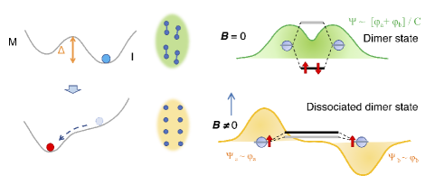
The Mott–Hubbard insulator is a class of materials in which strong electron correlation disturbs the motion of electrons and electrons are localised [9]. The magnetic ground state of many Mott-Hubbard insulators shows antiferromagnetic order, and high- superconductivity occurs near the magnetic-order phase, indicating that the spin degree of freedom is important to understand their peculiar electronic states. On the other hand, several insulators possess strong electron correlation, but their magnetic ground state is a spin singlet (nonmagnetic) [9]. VO2 is one such material. Strong electron correlation has been claimed to be necessary for understanding the large energy gap of 0.7 eV in the low-temperature insulating phase of VO2 [2, 3, 4]. A key feature of the MI transition of VO2 is that it occurs along with a structural transition from a high-temperature rutile (tetragonal) phase to a low-temperature monoclinic phase [1, 7, 8]. Vanadium dimers are formed in the low-temperature monoclinic phase, and electrons of the V ions (V4+: ) form metal–metal bonding with a molecular orbital. The electrons are localised in the molecular orbital of the V–V dimer, which can result in the insulating nature [5, 6, 7, 8].
Many theoretical and experimental studies have been conducted to determine whether the structural instability due to dimerisation [5, 6, 7, 8] or electron correlation (Mott physics) [2, 3, 10, 4, 11] is the more essential driving force behind the MI transition. Understanding of the microscopic mechanism of the MI transition of VO2 is also important for its practical applications as sensors and switching devices; abrupt changes in resistivity and optical absorption at the transition temperature 340 K are useful for them [12]. The manipulation of electron spins by a magnetic field can shed light on the problem of MI transition because the dimerisation can be suppressed by the Zeeman energy in magnetic fields. One may envision that the molecular orbital between the V atoms collapses by the forced alignment of the spin direction because the bonding orbital is formed only with two electrons having opposite spin states. The advantage of utilising a magnetic field is that the electronic state can be modified through the Zeeman splitting while maintaining the quantum-mechanical electron correlation that is significant at low temperatures. Since the Mott–Hubbard gap is expected to be insensitive to the spin state, the magnetic field cannot affect the insulating nature if the Mott physics is the more essential driving force behind the MI transition. Ultrahigh magnetic fields with Zeeman energy at least comparable to the thermal energy at the MI transition temperature () would be required to investigate the potential magnetic-field-induced metallisation of VO2.
In the present study, we experimentally demonstrate that the insulating dimerised state can be transformed to a metallic state by a strong magnetic field of 500 T in W-doped VO2, the MI transition temperature of which is controlled to approximately 100 K [13]. We performed magneto-transmission experiments using a near-infrared laser line and found a significant decrease in the transmitted light intensity at the ultrahigh-magnetic-field region, which is distinct evidence of the field-induced insulator–metal (IM) transition. The observed onset field of the transition at 14 K is approximately 120 T, and its Zeeman energy corresponds to 162 K when = 2 and = 1/2, where and are the -factor and spin quantum number, respectively. The observed magnetic-field-induced metallisation indicates that the dimerisation is a more essential driving force than the electron correlation for the MI transition in VO2.
Figure 1 shows optical absorption spectra of a V1-xWxO2 ( = 0.06) thin film at different temperatures without external magnetic fields. The broad absorption peak around 1 eV can be attributed to the excitation from the bonding orbital to the non-bonding orbital of the electrons of V4+ () in the octahedron of oxygen ions [14, 7, 15, 16]. The and orbitals originate from the state in the crystal field with cubic symmetry. The strong increase in absorption with photon energy increasing beyond approximately 1.8 eV is attributed to the transition of charge transfer from the vanadium 3-like band to the oxygen 2-like band [15].
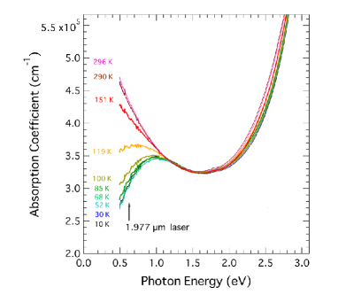
The absorption below approximately 1.2 eV is found to increase with decreasing photon energy at a high temperature of, e.g., 296 K. The absorption becomes less significant as the temperature decreases. This behaviour is accounted for by the opening of the energy gap and a change in the number of conduction electrons [15, 17]. The significant decrease of absorption with decreasing temperature at energies such as 0.627 eV (corresponding to the laser line wavelength of 1.977 m used for the magneto-transmission experiment) directly reflects the MI transition. The observed temperature dependence of the spectra is very similar to the previously reported result for V1-xWxO2 () [17].
Figures 2 (a) and (b) show, respectively, the temperature dependence of electrical resistivity () and that of the optical transmission at 1.977 m of three layers of a V1-xWxO2 () thin film with a total thickness of 45 nm.
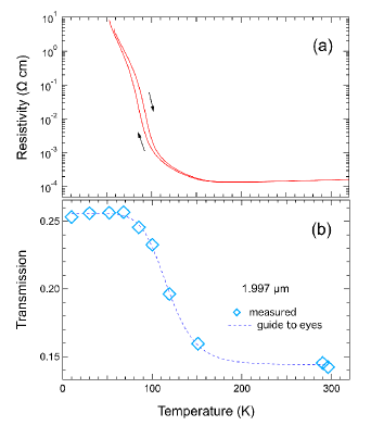
The MI transition occurs around 100 K, and the transmission below approximately 70 K is nearly independent of temperature. The curve-fitting analysis of the spectra, taking into account the DC electrical resistivity, shows that the effect of closing of the energy gap (change in the absorption band) is more significant than that of the free-carrier absorption. When the carrier density is less than approximately 1025 m-3, the transmission at 0.627 eV is nearly independent of the carrier density. Details of the fitting are described in the Supplementary Information. The hysteresis observed in the temperature dependence of indicates the first-order nature of the MI transition, although it is not observed very clearly in the temperature dependence of the transmission. The transmission is measured with both cooling and heating processes, and Fig. 2 (b) plots the averaged results.
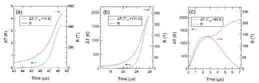
Ultrahigh magnetic fields () of up to 520 T are applied perpendicular to the thin-film plane (, where is the crystal axis of the rutile structure), and the optical transmission at 1.977 m is simultaneously measured. As shown in the upper panel of Fig. 3, the magnetic field (red curve) increases with time () and reaches 520 T at 42.8 s after the ignition of gap switches of the capacitor bank power supply at .
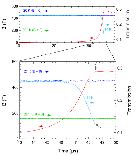
Figure 3 shows the evolution of the transmitted light intensity at 14 K with a light-blue curve. The lower panel of the figure shows a magnified view of the region from 50 to 520 T. The optical transmission at 20 and 291 K without magnetic fields is measured immediately before conducting the destructive ultrahigh-magnetic-field experiment, clearly showing the transmission levels in the insulating and metallic phases, respectively.
The transmission at 14 K under a magnetic field starts to show a gradual decrease at approximately 45 s when the magnetic field reaches approximately 100 T; subsequently, the decrease is accelerated with increasing magnetic field. Then eventually, the transmission under fields greater than 500 T is less than that in the high-temperature metallic phase (291 K), which clearly shows that the insulating phase of V1-xWxO2 () is transformed to a metallic phase under ultrahigh magnetic fields exceeding 500 T. Because the transmission at 14 K keeps decreasing beyond the value corresponding to the high-temperature metallic phase, the electrical resistivity is expected to be lower in the high-field metallic phase than in the high-temperature metallic phase. A lower scattering rate of electrons is expected owing to reductions in phonon and magnetic scattering in the novel low-temperature high-magnetic-field metallic phase.
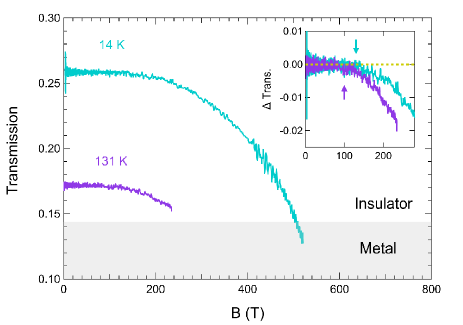
Figure 4 plots the transmission at 14 and 131 K as functions of the magnetic field. Because the experiment at 131 K was performed with a lower energy for magnetic-field generation, the maximum field was 240 T. The transmission at zero field is lower than that at 14 K because the temperature is close to . The inset shows the change in the transmission () as a function of the magnetic field. is found to become finite at a certain magnetic field (), as indicated by the arrow for each temperature. is evaluated as approximately 120 and 100 T at 14 and 131 K, respectively.
The optical absorption spectra shown in Fig. 1 and their temperature dependence are similar to those of VO2 [15] and in good agreement with previous results for V1-xWxO2 thin films [17]. The significant temperature dependence in the spectra at energies less than approximately 1.2 eV is due to the change in the energy band structure associated with the absorption arising from the transition and due to enhancement in free-carrier absorption, called Drude absorption, at high temperatures. Because the lowest photon energy in this work is 0.5 eV, the onset of the absorption corresponding to the energy gap is not observed. According to previous work [17], the energy gap for =0.06 is expected to be approximately 0.1 eV.
The considerable decrease of optical transmission at 1.977 m under an ultrahigh magnetic field, as shown in Fig. 4, constitutes direct evidence of a magnetic-field-induced IM (MFI-IM) transition. Because the transmission change is induced at a threshold magnetic field , the MFI-IM transition is likely a first-order transition. The transition is much broader than expected for a first-order transition because the inhomogeneous distribution of W sites [19] creates several nanoscale domains with slightly different potential barriers.
It would not be unreasonable to expect potential barriers between the metallic phase with a uniform V-atom distribution and the insulating phase with V–V dimers. The dimers are stabilised with the formation of metal–metal bonding, and the dimer can be regarded as a diatomic molecule [5, 8]. As schematically shown in Fig. 5, one of the most plausible explanations for the observed MFI-IM is that the V–V dimers are dissociated by the collapse of the molecular orbital. Because the molecular orbital is stable owing to the occupation of two electrons in the bonding sate and their spins need to be antiparallel, making the spins of the two electrons parallel can disturb the formation of bonding between adjacent V atoms. The spin quantum number of V4+ () is = 1/2, and its Zeeman energy at 120 T corresponds to 162 K, which is close to the onset temperature for the MI transition at zero magnetic field, as shown in Fig. 2. This fact supports the interpretation above. The potential barrier in Fig. 5 for the MFI-IM transition is expected to be as large as the Zeeman energy at 120 T. In contrast, the energy separation of the bonding and anti-bonding orbitals of the V–V dimer is expected to be approximately 2.5 eV [20, 7]. Because this energy scale corresponds to 30,000 K, which is more than two orders of magnitude larger than the Zeeman energy, the observed magnetic-field-induced metallisation cannot be explained by considering only an isolated single dimer. Some many-body interactions through the electron correlation [10, 4] would be necessary to understand the mechanism of dissociation of the dimers by controlling the electron spins.
Here, it is worth noting how the W doping affects the basic properties of VO2. As shown for the V1-xWxO2 () thin film investigated in this work, doping the V sublattice with W reduces the MI transition temperature by 20 K/at.%W for the bulk [21] and by 50 K/at.%W for nanostructures [13, 22]. The microscopic origin of the reduced was revealed by the extended X-ray absorption fine structure as follows. The local lattice structure at W sites is more symmetric than that at V sites and induces the detwisting of the nearby asymmetric monoclinic VO2 lattice towards the rutile phase [19]. The W sites form rutile-like VO2 nuclei, and the propagation of these nuclei decreases the energy barrier of the phase transition [19]. Hence, the intrinsic mechanism of the MI transition of W-doped VO2 is identical to that of non-doped VO2. The broadening of the transition found in the temperature dependence of the electrical resistivity is considered to be due to the inhomogeneous distribution of W sites and reflects the growing so-called “metallic puddles” in the insulating host [19, 23, 24]. Additionally, the growing part of the metallic puddles gradually reduces the optical transmission.
Another important issue regarding the reliability of the experimental results is the temperature of the sample in pulsed ultrahigh magnetic fields. When the sample is electrically conducting, eddy currents can heat it up. Because the pulse duration of the magnetic field in the present work is of the microsecond order, the time derivative of the magnetic field is large and may induce a significant increase in the sample temperature. We evaluated the temperature rise of the sample when it is in the insulating phase and found that the temperature rise is less than 4 K even at 500 T. We also found that even after the MFI-IM transition occurs and the resistivity becomes low, the temperature does not increase, because of fast thermal relaxation due to the very small thickness of the sample (15 nm). The nearly isothermal condition of the sample under a magnetic field has been experimentally proven by using a pulsed magnetic field with different time evolutions (a field generated by the single-turn-coil technique [25]). Although the calculated temperature quickly increases immediately after applying the magnetic field and reaches 300 K at 10 T when the sample temperature is 95 K, the measured optical transmission is almost constant up to approximately 100 T, indicating that no significant eddy-current heating occurs. A detailed discussion and evaluation of the sample temperature are presented in the Supplementary Information. The sample temperature is maintained even after the MFI-IM transition, and the isothermal process of the magnetic-field-induced phase transition has been measured in the present study.
In summary, we demonstrated that an ultrahigh magnetic field of 500 T can transform the insulating dimerised state of W-doped VO2 to a metallic state at low temperatures. We showed that the V–V dimers are dissociated by the collapse of the molecular orbital; the bonding state becomes unstable with the aligning of electron spins in the magnetic-field direction. The electrons participating in the metal–metal bonding becomes itinerant after the breaking of the dimers. This phenomenon is similar to “chemical catastrophe”: the chemical bonding is collapsed by a very strong magnetic field through the spin Zeeman effect [26, 27]. It had been considered to occur only in cosmic spaces such as on a neutron star, where a very strong magnetic field exceeding 106 T exists. The present work suggests that the formation of the molecular orbital between the vanadium ions, which results in the localisation of the unpaired electrons, is the predominant driving force behind the MI transition. On the other hand, the Zeeman energy corresponding to 500 T is approximately 60 meV, which is less than the eV-order binding energy for a local isolated V–V dimer by more than two orders of magnitude. Therefore, it is likely that the electronic correlation must also be included to obtain a quantitative understanding of the MFI-IM transition [10, 4].
From the perspective of material science, because a singlet spin state with the formation of a cluster of magnetic atoms is exhibited by various other strongly correlated insulators, such as Ti2O3 [28, 29], AlV2O4 [30], and CuIr2S4 [31], investigation of the effect of a magnetic field on their electronic states is an intriguing and important research problem. A magnetic field of the order of 1000 T is inevitable for such research because of their high of several hundreds of kelvins [9].
I Methods
A thin film of V1-xWxO2 () was prepared using pulsed laser deposition on a TiO2 (001) substrate [32]. The film has a 001-oriented single phase, and its thickness is 15 nm. The optical absorption spectra at zero field and different temperatures are acquired using a commercial spectrometer (JASCO V570) in the transmission configuration. The temperature dependence of the electrical resistivity was measured using the conventional four-probe method. Magneto-transmission measurements were performed using an infrared fibre laser (AdValue Photonics : AP-TM-1975-SM-05) having a wavelength of 1.977 m. A HgCdTe photodiode was used for detecting the intensity of the transmitted light. A 1000 T field generator using electromagnetic flux compression [18] was employed to obtain a strong magnetic field of 520 T. The infrared laser and HgCdTe detector were placed in a shield room to avoid electromagnetic noise during the magnetic-field generation. The sample has an area of mm2, and it is sandwiched by two optical fibres having a core diameter of 800 m, which are used for relaying incoming and transmitted laser light. Helium-flow-type cryostats made of plastic were used to achieve low temperatures for the magneto-transmission experiments under ultrahigh magnetic fields.
II Acknowledgements
This work was supported by a JSPS KAKENHI Grant-in-Aid for Challenging Exploratory Research under Grant Number 18K18728.
III Author contributions
Y.H.M. conceptualised the experiment. Y.H.M., D.N., A.I., and S.T. performed the optical spectroscopy and ultrahigh-magnetic-field magneto-transmission experiments. Y.M. and Y.S. performed crystal synthesis and electrical resistivity measurements. Y.H.M. performed data analysis and wrote the manuscript with input from all co-authors.
IV Supplementary Information
IV.1 Evaluation of heating of the sample in pulsed magnetic fields
When pulsed magnetic fields are applied to an electrically conducting sample, the sample temperature () can change with magnetic field () due to the eddy current heating. Here we evaluate the temperature rise () of a V1-xWxO2 ( = 0.06) thin film in ultrahigh pulsed magnetic fields. The is calculated as follows,
| (1) |
,where , , and are the radius, specific heat, and electrical resistivity of the sample, respectively. The calculated at different measurement conditions are shown in Figs. 6 (a), (b), and (c).
The is 0.9 mm and is assumed to be , where J/(m3 K4) is obtained from =2 MJ/(m3 K) at 300 K for VO2 [33]. The and used are shown in Table 1.
| 14 K | 95 K | 131 K | |
|---|---|---|---|
| [m] | 10 | 6 | |
| [J/(m3 K)] | 200 | 6 |
As shown in Fig. 6 (a), the is found to be smaller than 4 K if the initial temperature = 14 K even at 500 T. Hence the significant change in the optical transmission observed in high magnetic fields exceeding 120 T when = 14 K cannot be attributed to the effect of the eddy current heating.
On the other hand, the calculated for = 131 K in of up to 240 T (Fig. 6 (b)) suggests that significant heating of the sample takes place. It is because the is rather small reflecting metallic nature. The calculated reaches 100 K even at a low field of around 60 T. However, the experimentally obtained optical transmission is found to show nearly no dependence when the field is lower than 100 T, which indicates that the actual is smaller than a few Kelvin.
The similar finding is obtained from another experiment using the single-turn coil technique [25]. The waveform of is different from the one obtained by electromagnetic flux compression. As shown in Fig. 6 (c), the sinusoidal like curve can induce the eddy current heating just after application of field. The corresponding optical transmission experiment was conducted on the V1-xWxO2 ( = 0.06) thin film at 95 K. Fig. 7 (a) shows the time evolution of and that of transmission at 1.977 m.
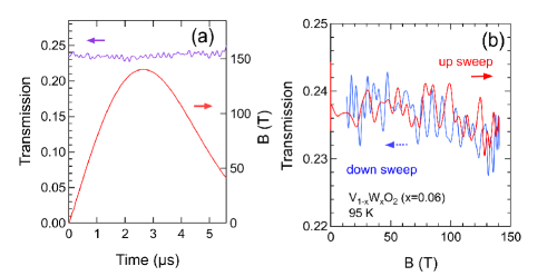
A significant decrease of the transmission is expected from the calculated because the temperature of the sample becomes 300 K at 10 T. One find, however, that the transmission keeps the initial value up to around 100 T. Moreover, a slight decrease of the transmission observed at field exceeding 100 T (Fig. 7 (b)) agrees with the results of higher field experiments up to 240 and 520 T.
From the experimental findings that transmission at 95 K and 131 K seem to be free from eddy-current heating, we can conclude that the calculated with adiabatic condition shown in Fig. 6 considerably overestimate the effect of sample heating. It should be taken into account transferring heat from the sample to the surrounding heat bath. In the present study, the heat generated in the sample actually can diffuse to the TiO2 substrate and the heat transfer can be very fast because the thickness of the V1-xWxO2 ( = 0.06) film () is only 15 nm. Insulating and nonmagnetic TiO2 substrate of which thickness is 0.5 mm would work as an ideal thermal bath.
The speed of the temperature transportation of the sample with the surface area and volume can be evaluated as follows using the Fourier’s law,
| (2) |
, where is the thermal conductivity. The speed is proportional to the gradient of the temperature in space . Here = 15 nm, and can be taken to be 20 W/(m K) for metallic VO2 [33].
To obtain isothermal condition for measurements, it is required to obtain thermal equilibrium condition by fast heat exchange with surrounding thermal bath. Considering = 1 K at the surface of the film, the distance between the surface and the substrate of 15 nm gives the relation
| (3) |
Then we have,
| (4) |
This is the speed of temperature transfer. Temperature increase of 1 K at the surface can be transferred to the interface between the sample and the TiO2 substrate in s 2.2 s = 22 ps. This time scale is six orders of magnitude smaller than the duration time of the magnetic field and thus the isothermal condition is expected to be maintained during the pulse. This fast thermal relaxation can explain the experimental findings that the isothermal condition is likely to be maintained during the microsecond ultrahigh pulse.
IV.2 Curve fitting of the absorption spectra at different temperatures
The optical absorption spectra of the V1-xWxO2 ( = 0.06) thin film are analyzed. In the insulating phase, as shown in Fig. 8 (a), the spectrum exhibits a clear absorption band around 1 eV and another absorption rise starts at around 2 eV indicating larger absorption band at higher energy. According to the previous studies [14, 7, 16], they are the absorption bands due to the and transitions, respectively. Here is the bonding orbital of the vanadium dimers and and are the orbitals originate from and orbitals. Because the is rather strongly hybridized with oxygen orbital, the latter transition can be regarded as a charge transfer (CT) absorption. On the other hand, has mostly and character of electrons of a vanadium atom [7]. A lognormal function is used for representing the transition contribution since the peak shape is asymmetric [15, 13], while a Gauss function is used to fit the slope of the the CT transition.
In addition to the two absorption bands, free carrier absorption (so-called Drude absorption) is taken into account for the spectra fitting. The absorption coefficient for the Drude component is expressed as follows.
| (5) |
Here, the plasma frequency is proportional to the square root of the carrier density .
| (6) |
is the wavelength, is the speed of light, is the reflective index, and is the scattering time. and are the dielectric constant of vacuum and the effective mass, respectively. [15, 34, 35] and =3 [36] are used for the fitting, where the is the free electron mass.
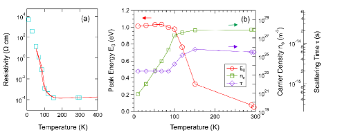
The representative optical absorption spectra at 10, 119, and 296 K are shown in Fig. 8 along with the fitting curves. The red curve is the result of the fitting. The green and purple curves are the components of and the CT transitions, respectively. The peak energy of the Lognormal function () seems to change with temperature, suggesting significant change in the electronic structure due to the metal-insulator transition of this sample around 100 K.
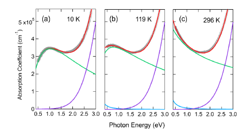
The Drude term is not significant at temperatures lower than around 70 K at which the is estimated to be around m-3. At higher temperatures, the Drude term contributes the optical absorption (light blue curve in Fig. 8). Because there are a lot of adjustable parameters and the slope due to the CT transition seems to be rather independent of temperature, we assume that the CT transition does not depend on temperature. Regarding the Drude absorption, we tried to find and that give a good fitting results and simultaneously explains the DC electrical resistivity shown in Fig. 9 (a).
The DC electrical resistivity is assumed to be expressed as follows.
| (7) |
The light-blue open squares shown in Fig. 9 (a) are the evaluated with the parameters used for the curve fitting for the optical absorption spectra. The parameters used are shown in Fig. 9 (b) as a function of temperature. Although the Drude theorem can be too simple to evaluate the electronic state of V1-xWxO2 ( = 0.06), the obtained at higher temperature around 1028 m-3 is in agreement with the expected carrier density 1.7 1028 m-3 assuming one electron per formula unit of VO2. (Here we use the density 2.33 g/cm3 and effects of W-doping is not taken into account.) Because the scattering time of carriers in metallic VO2 can be estimated as an order of s-1 [15], the shown in Fig. 9 (b) also seem be rather reasonable values .
As shown in the results of the curve fitting (Fig. 8), it is found that the contribution to the absorption at 0.627 eV (1.977 m) in the spectra of V1-xWxO2 ( = 0.06) mainly comes from the absorption due to the transition with a small contribution of the free carrier absorption. Therefore, the observed significant decrease of the transmission at 1.977 m in the ultrahigh magnetic fields exceeding 100 T to 520 T can be attributed to the change in the electronic state. The absorption band shifts to the lower energy with magnetic field and most probably close the energy gap at around 500 T.
References
- Morin [1959] F. J. Morin, Oxides which show a metal-to-insulator transition at the neel temperature, Phys. Rev. Lett. 3, 34 (1959).
- Zylbersztejn and Mott [1975] A. Zylbersztejn and N. F. Mott, Metal-insulator transition in vanadium dioxide, Phys. Rev. B 11, 4383 (1975).
- Rice et al. [1994] T. M. Rice, H. Launois, and J. P. Pouget, Comment on ”vo2: Peierls or mott-hubbard? a view from band theory”, Phys. Rev. Lett. 73, 3042 (1994).
- Huffman et al. [2017] T. J. Huffman, C. Hendriks, E. J. Walter, J. Yoon, H. Ju, R. Smith, G. L. Carr, H. Krakauer, and M. M. Qazilbash, Insulating phases of vanadium dioxide are mott-hubbard insulators, Phys. Rev. B 95, 075125 (2017).
- Goodenough [1960] J. B. Goodenough, Direct cation- -cation interactions in several oxides, Phys. Rev. 117, 1442 (1960).
- Wentzcovitch et al. [1994] R. M. Wentzcovitch, W. W. Schulz, and P. B. Allen, : Peierls or mott-hubbard? a view from band theory, Phys. Rev. Lett. 72, 3389 (1994).
- Eyert [2002] V. Eyert, The metal-insulator transitions of v: A band theoretical approach, Annalen der Physik 11, 650 (2002).
- Hiroi [2015] A. Hiroi, Structural instability of the rutile compounds and its relevance to the metal-insulator transition of vo2, Progress in Solid State Chemistry 43, 47 (2015).
- Imada et al. [1998] M. Imada, A. Fujimori, and Y. Tokura, Metal-insulator transitions, Rev. Mod. Phys. 70, 1039 (1998).
- Biermann et al. [2005] S. Biermann, A. Poteryaev, A. I. Lichtenstein, and A. Georges, Dynamical singlets and correlation-assisted peierls transition in , Phys. Rev. Lett. 94, 026404 (2005).
- Najera et al. [2017] O. Najera, M. Civelli, V. Dobrosavljevic, and M. J. Rozenberg, Resolving the controversy: Mott mechanism dominates the insulator-to-metal transition, Phys. Rev. B 95, 035113 (2017).
- Jia et al. [2018] Z.-Y. Jia, F.-Z. Shu, Y.-J. Gao, F. Cheng, R.-W. Peng, R.-H. Fan, Y. Liu, and M. Wang, Dynamically switching the polarization state of light based on the phase transition of vanadium dioxide, Phys. Rev. Applied 9, 034009 (2018).
- Shibuya et al. [2010] K. Shibuya, M. Kawasaki, and Y. Tokura, Metal-insulator transition in epitaxial () thin films, Applied Physics Letters 96, 022102 (2010).
- Gavini and Kwan [1972] A. Gavini and C. C. Y. Kwan, Optical properties of semiconducting films, Phys. Rev. B 5, 3138 (1972).
- Okazaki et al. [2006] K. Okazaki, S. Sugai, Y. Muraoka, and Z. Hiroi, Role of electron-electron and electron-phonon interaction effects in the optical conductivity of , Phys. Rev. B 73, 165116 (2006).
- He et al. [2016] H. He, A. X. Gray, P. Granitzka, J. W. Jeong, N. P. Aetukuri, R. Kukreja, L. Miao, S. A. Breitweiser, J. Wu, Y. B. Huang, P. Olalde-Velasco, J. Pelliciari, W. F. Schlotter, E. Arenholz, T. Schmitt, M. G. Samant, S. S. P. Parkin, H. A. Dürr, and L. A. Wray, Measurement of collective excitations in by resonant inelastic x-ray scattering, Phys. Rev. B 94, 161119 (2016).
- Lee et al. [2012] J. S. Lee, K. Shibuya, M. Kawasaki, and Y. Tokura, Optical investigation of metal-insulator transitions in v1-xwxo2 (0 0.33), Phys. Rev. B 85, 155110 (2012).
- Nakamura et al. [2018] D. Nakamura, A. Ikeda, H. Sawabe, Y. H. Matsuda, and S. Takeyama, Record indoor magnetic field of 1200 t generated by electromagnetic flux-compression, Review of Scientific Instruments 89, 095106 (2018).
- Tan et al. [2012] X. Tan, T. Yao, R. Long, Z. Sun, Y. Feng, H. Cheng, X. Yuan, W. Zhang, Q. Liu, C. Wu, and Y. X. andShiqiang Wei, Unraveling metal-insulator transition mechanism of triggered by tungsten doping, Scientific Reports 2, 466 (2012).
- Goodenough [1971] J. B. Goodenough, The two components of the crystallographic transition in vo2, Journal of Solid State Chemistry 3, 490 (1971).
- Horlin et al. [1972] T. Horlin, T. Niklewski, and M. Nygren, Electrical and magnetic properties of v1-xwxo2, , Materials Research Bulletin 7, 1515 (1972).
- Wu et al. [2011] T.-L. Wu, L. Whittaker, S. Banerjee, and G. Sambandamurthy, Temperature and voltage driven tunable metal-insulator transition in individual v1-xo2 nanowires, Phys. Rev. B 83, 073101 (2011).
- Qazilbash et al. [2007] M. M. Qazilbash, M. Brehm, B.-G. Chae, P.-C. Ho, G. O. Andreev, B.-J. Kim, S. J. Yun, A. V. Balatsky, M. B. Maple, F. Keilmann, H.-T. Kim, and D. N. Basov, Mott transition in vo2 revealed by infrared spectroscopy and nano-imaging, Science 318, 1750 (2007).
- Choi et al. [1996] H. S. Choi, J. S. Ahn, J. H. Jung, T. W. Noh, and D. H. Kim, Mid-infrared properties of a film near the metal-insulator transition, Phys. Rev. B 54, 4621 (1996).
- Miura et al. [2004] N. Miura, T. Osada, and S. Takeyama, Research in super-high pulsed magnetic fields at the megagauss laboratory of the university of tokyo, J. Low Temp. Phys 133, 139 (2004).
- Date [1995] M. Date, Recent progress in high field magnetism, Australian Journal of Physics 48, 187 (1995).
- Detmer et al. [1997] T. Detmer, P. Schmelcher, F. K. Diakonos, and L. S. Cederbaum, Hydrogen molecule in magnetic fields: The ground states of the manifold of the parallel configuration, Phys. Rev. A 56, 1825 (1997).
- Eyert et al. [2005] V. Eyert, U. Schwingenschl’́ogl, and U. Eckern, Covalent bonding and hybridization effect in the corundum-type transition-metal oxides v2o3 and ti2o3, Europhys. Lett. 70, 782 (2005).
- Chang et al. [2018] C. F. Chang, T. C. Koethe, Z. Hu, J. Weinen, S. Agrestini, L. Zhao, J. Gegner, H. Ott, G. Panaccione, H. Wu, M. W. Haverkort, H. Roth, A. C. Komarek, F. Offi, G. Monaco, Y.-F. Liao, K.-D. Tsuei, H.-J. Lin, C. T. Chen, A. Tanaka, and L. H. Tjeng, -axis dimer and its electronic breakup: The insulator-to-metal transition in , Phys. Rev. X 8, 021004 (2018).
- Horibe et al. [2006] Y. Horibe, M. Shingu, K. Kurushima, H. Ishibashi, N. Ikeda, K. Kato, Y. Motome, N. Furukawa, S. Mori, and T. Katsufuji, Spontaneous formation of vanadium “molecules” in a geometrically frustrated crystal: , Phys. Rev. Lett. 96, 086406 (2006).
- Radaelli et al. [2002] P. G. Radaelli, Y. Horibe, M. J. Gutmann, H. Ishibashi, C. H. Chen, R. M. Ibberson, Y. Koyama, Y.-S. Hor, V. Kiryukhin, and S.-W. Cheong, Formation of isomorphic ir3+ and ir4+ octamers and spin dimerization in the spinel cuir2s4, Nature 416, 155 (2002).
- Muraoka and Hiroi [2002] Y. Muraoka and Z. Hiroi, Metal-insulator transition of thin films grown on (001) and (110) substrates, Applied Physics Letters 80, 583 (2002).
- Hamaoui et al. [2019] G. Hamaoui, N. Horny, C. Gomez-Heredia, J. Ramirez-Rincon, J. Ordonez-Miranda, C. Champeaux, F. Dumas-Bouchiat, J. Alvarado-Gil, Y. Ezzahri, J. K., and M. Chirtoc, Thermophysical characterisation of v thin films hysteresis and its application in thermal rectification, Sci. Rep. 9, 8728 1 (2019).
- Brito et al. [2016] W. H. Brito, M. C. O. Aguiar, K. Haule, and G. Kotliar, Metal-insulator transition in : A perspective, Phys. Rev. Lett. 117, 056402 (2016).
- Muraoka et al. [2018] Y. Muraoka, H. Nagao, Y. Yao, T. Wakita, K. Terashima, T. Yokoya, H. Kumigashira, and M. Oshima, Fermi surface topology in a metallic phase of v thin films grown on tio2(001) substrates, Sci. Rep. 8, 17906 (2018).
- Verleur et al. [1968] H. W. Verleur, A. S. Barker, and C. N. Berglund, Optical properties of v between 0.25 and 5 ev, Phys. Rev. 172, 788 (1968).