Exfoliated hexagonal BN as gate dielectric for InSb nanowire quantum dots with improved gate hysteresis and charge noise
Abstract
We characterize InSb quantum dots induced by bottom finger gates within a nanowire that is grown via the vapor-liquid-solid process. The gates are separated from the nanowire by an exfoliated 35 nm thin hexagonal BN flake. We probe the Coulomb diamonds of the gate induced quantum dot exhibiting charging energies of meV and orbital excitation energies up to meV. The gate hysteresis for sweeps covering 5 Coulomb diamonds reveals an energy hysteresis of only µeV between upwards and downwards sweeps. Charge noise is studied via long-term measurements at the slope of a Coulomb peak revealing potential fluctuations of 1 µeV/ at 1 Hz. This makes h-BN the dielectric with the currently lowest gate hysteresis and lowest low-frequency potential fluctuations reported for low-gap III-V nanowires. The extracted values are similar to state-of-the art quantum dots within Si/SiGe and Si/SiO2 systems.
Recently, nanowires (NW) of InSb and InAs Hiruma et al. (1995); Jensen et al. (2004); Björk et al. (2002); Borg and Wernersson (2013) came back into focus due to their large spin-orbit coupling Nilsson et al. (2009); Nadj-Perge et al. (2010); Fasth et al. (2007) that in combination with magnetic fields and a relatively strong proximity-induced superconductivityDoh et al. (2005); Takayanagi and Kawakami (1985); Nilsson et al. (2012) enables tuning of Majorana modes Alicea (2012); Mourik et al. (2012); Albrecht et al. (2016); Lutchyn et al. (2018) as a basis for topologically protected quantum computing. Stern and Lindner (2013); Vijay, Hsieh, and Fu (2015); Litinski et al. (2017) Typically, the NWs are tuned electrically by a number of bottom finger gates that are separated from the NW by a gate dielectric.Mourik et al. (2012); Das et al. (2012) It is well known that both charge noise and hysteresis of gate-induced potentials deteriorate the performance of semiconductor qubits, Culcer, Hu, and Sarma (2009); Kuhlmann et al. (2013); Yoneda et al. (2017); Mi, Kohler, and Petta (2018) as is also expected for the prospective Majorana qubits.Schmidt, Rainis, and Loss (2012); Li et al. (2018) Hence, it is crucial to optimize the dielectric in terms of unintentional charge fluctuations.
For exfoliated two-dimensional materials such as graphene, it turned out that hexagonal boron nitride (h-BN) is ideal for that purpose. Geim and Grigorieva (2013); Frisenda et al. (2018) For example, it improves the charge carrier mobility by more than an order of magnitude compared to the previously used Si/SiO2.Dean et al. (2010); Banszerus et al. (2016) Furthermore, it is easy to fabricate. Thus, exploiting exfoliated h-BN as gate dielectric for low-gap III-V NWs is appealing. First experiments used h-BN to separate the global Si/SiO2 back gate from an InSb NW enabling the first quantized conductance steps in such NWs at zero magnetic field.Kammhuber et al. (2016) Subsequently, measurements on proximity-coupled InSb NWs on h-BN showed magnetic field induced zero bias peaks, indicative of the presence of Majorana zero modes.Gül et al. (2018); Gill et al. (2018) However, Coulomb diamonds (CDs) with excited states in a gate-induced quantum dot (QD) have not been reported and, more importantly, the charge noise and gate hysteresis of such NWs on h-BN have not been studied. Reports on these properties are only available for other types of dielectrics. Sakr and Gao (2008); Nilsson et al. (2008); Delker et al. (2012); Vitusevich and Zadorozhnyi (2017); Delker et al. (2013); Petrychuk et al. (2019); Persson, Malm, and Wernersson (2013); Persson et al. (2010); Wahl et al. (2013); Volk et al. (2010); Gül et al. (2015) They exhibit, e.g., a relatively large low-temperature gate hysteresis on LaLuO3 and SiO2 being V and V at gate sweep ranges of 4 V and 30 V, respectively.Volk et al. (2010); Gül et al. (2015) Noise properties for QDs have only been reported for a vacuum dielectric revealing behavior above 300 Hz and an upturn at lower frequency with noise of µeV at 100 Hz.Nilsson et al. (2008)
Here, we study an InSb NW/h-BN device with bottom finger gates (pitch 90 nm) at the temperature mK. The device exhibits a gate hysteresis of 2 mV for sweeps of 150 mV (250 mV) at a rate of 25 mV/s (42 mV/h), hence, significantly better than in previous reports.Volk et al. (2010); Gül et al. (2015) It, moreover, shows a charge noise of only 1 µeV at Hz with an approximate dependence towards lower frequencies. The noise is similar to the previously studied vacuum dielectricNilsson et al. (2008) pointing to remaining limitations due to defects at the NW itself. More importantly, the value is slightly better than for state-of-the-art QDs in Si/SiGe or Si/SiO2 structures ( µeV at Hz). Freeman, Schoenfield, and Jiang (2016); Petit et al. (2018); Connors et al. (2019); Mi, Kohler, and Petta (2018) Hence, h-BN turns out to be a favorable dielectric for low-gap III-V NWs.
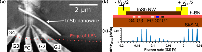
The InSb NWs were grown on top of InP stems via the vapor-liquid-solid (VLS) method using a gold droplet as catalyst.Plissard et al. (2012); Car et al. (2014) A QD device of such a NW (Fig. 1(a)(b)) consists of a 200 nm thick SiNx layer, on a highly doped Si substrate acting as a global back gate (BG) with multiple finger gates (G1G4, FG) on top. The finger gates are 35 nm wide and defined by electron beam lithography (EBL) with a spacing of 55 nm except between G3 and FG where the spacing is 130 nm. An h-BN flake is deposited on top of the finger gates via the dry transfer method.Dean et al. (2010) Subsequently, one InSb NW is placed onto the h-BN with sub-µm lateral precision via an indium tip attached to a micromanipulator. Flöhr et al. (2011) Finally, source and drain contacts are prepared via EBL. Prior to the metal deposition of the Ti/Au (10 nm/110 nm) contacts, the exposed NW area is passivated ex-situ by sulphurSuyatin et al. (2007) and subsequently cleaned in-situ by argon ion bombardment. Transport measurements are performed at mK in a 3He magneto-cryostat (Teslatron from Oxford Instruments). Before cool-down, the insert is evacuated to mbar for 48 h at 300 K in order to remove adsorbates from the NW surface.Gül et al. (2015)
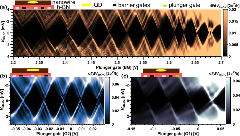
Gate dependent conductivity traces (not shown) reveal a low temperature mobility of the NW of cm2/Vs.Gül et al. (2015) Using the finger gates, we induce a QD within the NW exhibiting regularly spaced Coulomb peaks of different heights (Fig. 1(c)), probably due to different coupling of the states to the tunnel barriers. Different combinations of finger gates reveal charge stability diagrams of such QDs with regularly spaced CDs for all combinations of gates and excited states at larger (Fig. 2(a)-(c)). Only very few perturbations appear, likely caused by uncontrolled charging events in the surrounding of the QD. We could not measure the last CD prior to depletion probably due to the elongated QD geometry decoupling the lowest energy state from the tunnel barriers. For the CDs of Fig. 2(a)-(c), one straightforwardly deduces charging energies up to 3 meV, 2.3 meV, and 2.5 meV and lever arms of 0.05 eV/V, 0.12 eV/V, and 0.03 eV/V, respectively. Estimating the QD extension via the QD capacitance aF assuming, for the sake of simplicity, charging of an isolated sphere of radius , we reasonably find nm Shorubalko et al. (2007) using the dielectric constant of InSb . The deduced diameter is a bit smaller than gate spacing and NW diameter ( nm). This could partly be due to squeezing of the QD area in the direction perpendicular to the wire axis via the gate voltages as indeed found by COMSOL© simulations.Heedt et al. (2015)
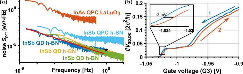
To quantify the charge noise acting on the NW QDs, Fig. 3(a) shows low-frequency noise measurements for the three different gate configurations. We measure the temporal current fluctuations at the slope of a Coulomb peak for µV. In order to transfer this to the potential fluctuation noise as function of frequency , we firstly use the measured shape of the Coulomb peak in traces, well fitted by a Fermi-Dirac peak, to deduce the gate voltage variation, . Then, we transfer to potential energy variation with as deduced from respective CDs. The square root of the single-sided power spectral density of the resulting in the QD leads to in eV/ as displayed in Fig. 3(a) with the rms potential noise being across the measurement bandwidth. We find Hz µeV and an increase towards lower mostly following (red fit line). The enhanced logarithmic slope of with respect to the classical noise is in reasonable agreement with the upturn of the noise below Hz observed earlier for InAs NWs with vacuum dielectric.Nilsson et al. (2008)
We also display a direct comparison of quantum point contacts (QPCs) for the InSb NW on hBN with an InAs NWDo et al. (2007) on a LaLuO3 dielectric. Except for the dielectric, deposited via pulsed laser deposition Volk et al. (2010), the two devices are prepared identically. The QPC is formed by charging one of the finger gates only with all other gates grounded. The displayed (Fig. 3(a), orange) originates from at the pinch-off of the NW induced by a single finger gate. It is converted to by the measured using eV/V for the hBN device as determined from the corresponding QD CDs with error bars as deduced from CD variations and eV/V for the LaLuO3 device deduced by scaling for the different thicknesses (hBN: nm, LaLuO3: nm) and for the different (hBN: Young et al. (2012), LaLuO3: 26 Schäfer et al. (2015)). Remarkably, of the h-BN device is more than two orders of magnitude lower than for the LaLuO3 device (Fig. 3(a)) illustrating the excellent properties of the hBN dielectric. We employed all four finger gates for such QPC measurements. The resulting curves are nearly identical up to 1 Hz, but vary at higher frequency being either lower by up to a factor of four or larger by up to a factor of three with respect to the displayed curve. This indicates the presence of particular fluctuators at Hz in the device Chanrion et al. (2020); Connors et al. (2019).
Comparison with literature data on noise for III-V low-gap NWs is difficult. Either much longer parts of the NW are gatedSakr and Gao (2008), effectively averaging charge fluctuations, or the frequencies are larger due to probing by radio frequency via reflection at the QD. Nilsson et al. (2008) Extrapolating the latter noise data obtained for a suspended InAs NW (vacuum dielectric) at 100 HzNilsson et al. (2008) towards Hz via the measured dependence leads to Hz µeV, larger than for our device on h-BN ( µeV at 10 Hz). However, the data with vacuum dielectric are measured at 1.5 K such that extrapolating to 0.3 K by the established linear temperature dependencePetit et al. (2018); Connors et al. (2019) yields Hz µeV, slightly better but still rather similar to our device. Since vacuum exhibits no defects acting as charge traps, Nilson et al.Nilsson et al. (2008) conjectured that the major charge noise originates from charge traps within or on the NW and not from the dielectric. Regarding the similarity of Hz, we believe that this is correct for our device, too.
It is instructive to compare our data with the charge noise in Si or Si/SiGe QDsConnors et al. (2019); Freeman, Schoenfield, and Jiang (2016); Petit et al. (2018); Mi, Kohler, and Petta (2018); Chanrion et al. (2020), currently considered as most promising for semiconductor spin qubitsWatson et al. (2018). For these QDs, one finds Hz with device-dependent and, consistently, an increase of with increasing . Favorably, the reported at 0.3 K (1-5 µeV at 1 Hz)Petit et al. (2018); Connors et al. (2019); Freeman, Schoenfield, and Jiang (2016); Chanrion et al. (2020) (star in Fig. 3(a)) is not smaller than for our InSb NW QD on h-BN ( µeV at 1 Hz). This renders the device competitive to the most favorable material combinations in terms of charge noise.
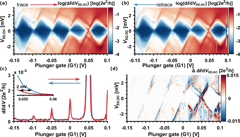
The second important benchmark for a dielectric is the gate hysteresis. Figure 3(b) reveals that the InSb NW on h-BN exhibits a gate hysteresis mV (inset) at a sweep rate of 25 mV/s. Since it is known that the hysteresis strongly depends on the probed gate range, we scale the hysteresis by the gate range for comparison. For the gate range mV, this leads to a ratio . This is much lower than observed previously for InAs or InSb NWs on other gate dielectrics: Volk et al. (2010), Gül et al. (2015), where higher temperatures (25 K, 4.2 K) have been employed that typically even reduce hysteresis as indeed found in one of these studies Volk et al. (2010). Since additionally depends on the sweep rateLynall et al. (2018); Dayeh et al. (2007), we improved it further by reducing the gate sweep rate to 42 mV/h leading to with mV. The extremely low rate is employed to record full charge stability diagrams subsequently for both gate sweep directions (Fig. 4(a),(b)). The total measurement time of 12 h evidences the long term stability of the QD by the excellent similarity of the two diagrams. Only two conductivity jumps (Fig. 4(b), right) are observed. The gate hysteresis is quantified by a line cut at mV (Fig. 4(c)) revealing mV as maximum hysteresis between the two curves (inset) and, hence, implying . Using eV/V, one can calculate the energy hysteresis µeV. Figure 4(d) displays the difference between Fig. 4(b) and Fig. 4(a) showing that the small hysteresis is reliably observed across the whole charge stability diagram. The observation of a small hysteresis, low charge noise and a small number of jumps in stability diagrams consistently indicate a very low number of chargeable impurities in the h-BN layer, thus making it a favorable dielectric for III-V NW devices. As pointed out above, the performance is likely limited by the remaining charge traps on the NW itself.
In summary, we have presented an InSb NW device with an h-BN flake as gate dielectric. With a set of finger gates, electrons are confined in QDs using different gate configurations, resulting in regular Coulomb diamonds with multiple excited states. Favorably, the device has the lowest noise level (1 µeV/ at Hz) reported for low-gap III-V NW devices yet and shows an unprecedented gate hysteresis of 2 mV only. Hence, in terms of charge noise, h-BN is the currently most favorable dielectric for low-gap III-V NW devices.
Acknowledgements.
We thank S. Trellenkamp and F. Lentz for help with the EBL and H. Bluhm for helpful discussions. Funding by the German Research Foundation (DFG) under Germany’s Excellence Strategy – Cluster of Excellence Matter and Light for Quantum Computing (ML4Q) EXC 2004/1 – 390534769 and by European Graphene Flagship Core 2, grant number 785219 is gratefully acknowledged.Data availability
The data that support the findings of this study are available from the corresponding author upon reasonable request.
References
- Hiruma et al. (1995) K. Hiruma, M. Yazawa, T. Katsuyama, K. Ogawa, K. Haraguchi, M. Koguchi, and H. Kakibayashi, J. Appl. Phys. 77, 447 (1995).
- Jensen et al. (2004) L. E. Jensen, M. T. Björk, S. Jeppesen, A. I. Persson, B. J. Ohlsson, and L. Samuelson, Nano Lett. 4, 1961 (2004).
- Björk et al. (2002) M. T. Björk, B. J. Ohlsson, C. Thelander, A. I. Persson, K. Deppert, L. R. Wallenberg, and L. Samuelson, Appl. Phys. Lett. 81, 4458 (2002).
- Borg and Wernersson (2013) B. M. Borg and L.-E. Wernersson, Nanotechnology 24, 202001 (2013).
- Nilsson et al. (2009) H. A. Nilsson, P. Caroff, C. Thelander, M. Larsson, J. B. Wagner, L.-E. Wernersson, L. Samuelson, and H. Q. Xu, Nano Lett. 9, 3151 (2009).
- Nadj-Perge et al. (2010) S. Nadj-Perge, S. M. Frolov, E. P. A. M. Bakkers, and L. P. Kouwenhoven, Nature 468, 1084 (2010).
- Fasth et al. (2007) C. Fasth, A. Fuhrer, L. Samuelson, V. N. Golovach, and D. Loss, Phys. Rev. Lett. 98, 266801 (2007).
- Doh et al. (2005) Y.-J. Doh, J. A. van Dam, A. L. Roest, E. P. A. M. Bakkers, L. P. Kouwenhoven, and S. D. Franceschi, Science 309, 272 (2005).
- Takayanagi and Kawakami (1985) H. Takayanagi and T. Kawakami, Phys. Rev. Lett. 54, 2449 (1985).
- Nilsson et al. (2012) H. A. Nilsson, P. Samuelsson, P. Caroff, and H. Q. Xu, Nano Lett. 12, 228 (2012).
- Alicea (2012) J. Alicea, Rep. Prog. Phys. 75, 076501 (2012).
- Mourik et al. (2012) V. Mourik, K. Zuo, S. M. Frolov, S. R. Plissard, E. P. A. M. Bakkers, and L. P. Kouwenhoven, Science 336, 1003 (2012).
- Albrecht et al. (2016) S. M. Albrecht, A. P. Higginbotham, M. Madsen, F. Kuemmeth, T. S. Jespersen, J. Nygård, P. Krogstrup, and C. M. Marcus, Nature 531, 206 (2016).
- Lutchyn et al. (2018) R. M. Lutchyn, E. P. A. M. Bakkers, L. P. Kouwenhoven, P. Krogstrup, C. M. Marcus, and Y. Oreg, Nat. Rev. Mater. 3, 52 (2018).
- Stern and Lindner (2013) A. Stern and N. H. Lindner, Science 339, 1179 (2013).
- Vijay, Hsieh, and Fu (2015) S. Vijay, T. H. Hsieh, and L. Fu, Phys. Rev. X 5, 041038 (2015).
- Litinski et al. (2017) D. Litinski, M. S. Kesselring, J. Eisert, and F. von Oppen, Phys. Rev. X 7, 031048 (2017).
- Das et al. (2012) A. Das, Y. Ronen, Y. Most, Y. Oreg, M. Heiblum, and H. Shtrikman, Nat. Phys. 8, 887 (2012).
- Culcer, Hu, and Sarma (2009) D. Culcer, X. Hu, and S. D. Sarma, Appl. Phys. Lett. 95, 073102 (2009).
- Kuhlmann et al. (2013) A. V. Kuhlmann, J. Houel, A. Ludwig, L. Greuter, D. Reuter, A. D. Wieck, M. Poggio, and R. J. Warburton, Nat. Phys. 9, 570 (2013).
- Yoneda et al. (2017) J. Yoneda, K. Takeda, T. Otsuka, T. Nakajima, M. R. Delbecq, G. Allison, T. Honda, T. Kodera, S. Oda, Y. Hoshi, N. Usami, K. M. Itoh, and S. Tarucha, Nat. Nanotechnol. 13, 102 (2017).
- Mi, Kohler, and Petta (2018) X. Mi, S. Kohler, and J. R. Petta, Phys. Rev. B 98, 161404 (2018).
- Schmidt, Rainis, and Loss (2012) M. J. Schmidt, D. Rainis, and D. Loss, Phys. Rev. B 86, 085414 (2012).
- Li et al. (2018) T. Li, W. A. Coish, M. Hell, K. Flensberg, and M. Leijnse, Phys. Rev. B 98, 205403 (2018).
- Geim and Grigorieva (2013) A. K. Geim and I. V. Grigorieva, Nature 499, 419 (2013).
- Frisenda et al. (2018) R. Frisenda, E. Navarro-Moratalla, P. Gant, D. P. D. Lara, P. Jarillo-Herrero, R. V. Gorbachev, and A. Castellanos-Gomez, Chem. Soc. Rev. 47, 53 (2018).
- Dean et al. (2010) C. R. Dean, A. F. Young, I. Meric, C. Lee, L. Wang, S. Sorgenfrei, K. Watanabe, T. Taniguchi, P. Kim, K. L. Shepard, and J. Hone, Nat. Nanotechnol. 5, 722 (2010).
- Banszerus et al. (2016) L. Banszerus, M. Schmitz, S. Engels, M. Goldsche, K. Watanabe, T. Taniguchi, B. Beschoten, and C. Stampfer, Nano Lett. 16, 1387 (2016).
- Kammhuber et al. (2016) J. Kammhuber, M. C. Cassidy, H. Zhang, Ö. Gül, F. Pei, M. W. A. de Moor, B. Nijholt, K. Watanabe, T. Taniguchi, D. Car, S. R. Plissard, E. P. A. M. Bakkers, and L. P. Kouwenhoven, Nano Lett. 16, 3482 (2016).
- Gül et al. (2018) Ö. Gül, H. Zhang, J. D. S. Bommer, M. W. A. de Moor, D. Car, S. R. Plissard, E. P. A. M. Bakkers, A. Geresdi, K. Watanabe, T. Taniguchi, and L. P. Kouwenhoven, Nat. Nanotechnol. 13, 192 (2018).
- Gill et al. (2018) S. T. Gill, J. Damasco, B. E. Janicek, M. S. Durkin, V. Humbert, S. Gazibegovic, D. Car, E. P. A. M. Bakkers, P. Y. Huang, and N. Mason, Nano Lett. 18, 6121 (2018).
- Sakr and Gao (2008) M. R. Sakr and X. P. A. Gao, Appl. Phys. Lett. 93, 203503 (2008).
- Nilsson et al. (2008) H. A. Nilsson, T. Duty, S. Abay, C. Wilson, J. B. Wagner, C. Thelander, P. Delsing, and L. Samuelson, Nano Lett. 8, 872 (2008).
- Delker et al. (2012) C. J. Delker, S. Kim, M. Borg, L. Wernersson, and D. B. Janes, IEEE T. Electron. Dev. 59, 1980 (2012).
- Vitusevich and Zadorozhnyi (2017) S. Vitusevich and I. Zadorozhnyi, Semicond. Sci. Tech. 32, 043002 (2017).
- Delker et al. (2013) C. J. Delker, Y. Zi, C. Yang, and D. B. Janes, IEEE T. Electron Dev. 60, 2900 (2013).
- Petrychuk et al. (2019) M. Petrychuk, I. Zadorozhnyi, Y. Kutovyi, S. Karg, H. Riel, and S. Vitusevich, Nanotechnology 30, 305001 (2019).
- Persson, Malm, and Wernersson (2013) K.-M. Persson, B. G. Malm, and L.-E. Wernersson, Appl. Phys. Lett. 103, 033508 (2013).
- Persson et al. (2010) K.-M. Persson, E. Lind, A. W. Dey, C. Thelander, H. Sjoland, and L.-E. Wernersson, IEEE Electr. Device L. 31, 428 (2010).
- Wahl et al. (2013) R. E. Wahl, F. Wang, H. E. Chung, G. R. Kunnen, S. Yip, E. H. Lee, E. Y. B. Pun, G. B. Raupp, D. R. Allee, and J. C. Ho, IEEE Electr. Device L. 34, 765 (2013).
- Volk et al. (2010) C. Volk, J. Schubert, M. Schnee, K. Weis, M. Akabori, K. Sladek, H. Hardtdegen, and Th. Schäpers, Semicond. Sci. Technol. 25, 085001 (2010).
- Gül et al. (2015) Ö. Gül, D. J. van Woerkom, I. van Weperen, D. Car, S. R. Plissard, E. P. A. M. Bakkers, and L. P. Kouwenhoven, Nanotechnology 26, 215202 (2015).
- Freeman, Schoenfield, and Jiang (2016) B. M. Freeman, J. S. Schoenfield, and H. Jiang, Appl. Phys. Lett. 108, 253108 (2016).
- Petit et al. (2018) L. Petit, J. Boter, H. Eenink, G. Droulers, M. Tagliaferri, R. Li, D. Franke, K. Singh, J. Clarke, R. Schouten, V. Dobrovitski, L. Vandersypen, and M. Veldhorst, Phys. Rev. Lett. 121, 076801 (2018).
- Connors et al. (2019) E. J. Connors, J. Nelson, H. Qiao, L. F. Edge, and J. M. Nichol, Phys. Rev. B 100, 165305 (2019).
- Plissard et al. (2012) S. R. Plissard, D. R. Slapak, M. A. Verheijen, M. Hocevar, G. W. G. Immink, I. van Weperen, S. Nadj-Perge, S. M. Frolov, L. P. Kouwenhoven, and E. P. A. M. Bakkers, Nano Lett. 12, 1794 (2012).
- Car et al. (2014) D. Car, J. Wang, M. A. Verheijen, E. P. A. M. Bakkers, and S. R. Plissard, Adv. Mater. 26, 4875 (2014).
- Flöhr et al. (2011) K. Flöhr, M. Liebmann, K. Sladek, H. Y. Günel, R. Frielinghaus, F. Haas, C. Meyer, H. Hardtdegen, Th. Schäpers, D. Grützmacher, and M. Morgenstern, Rev. Sci. Instrum. 82, 113705 (2011).
- Suyatin et al. (2007) D. B. Suyatin, C. Thelander, M. T. Björk, I. Maximov, and L. Samuelson, Nanotechnology 18, 105307 (2007).
- Shorubalko et al. (2007) I. Shorubalko, A. Pfund, R. Leturcq, M. T. Borgström, F. Gramm, E. Müller, E. Gini, and K. Ensslin, Nanotechnology 18, 044014 (2007).
- Heedt et al. (2015) S. Heedt, I. Otto, K. Sladek, H. Hardtdegen, J. Schubert, N. Demarina, H. Lüth, D. Grützmacher, and Th. Schäpers, Nanoscale 7, 18188 (2015).
- Do et al. (2007) Q.-T. Do, K. Blekker, I. Regolin, W. Prost, and F.-J. Tegude, IEEE Electr. Device L. 28, 682 (2007).
- Young et al. (2012) A. F. Young, C. R. Dean, I. Meric, S. Sorgenfrei, H. Ren, K. Watanabe, T. Taniguchi, J. Hone, K. L. Shepard, and P. Kim, Phys. Rev. B 85, 235458 (2012).
- Schäfer et al. (2015) A. Schäfer, F. Wendt, S. Mantl, H. Hardtdegen, M. Mikulics, J. Schubert, M. Luysberg, A. Besmehn, G. Niu, and T. Schroeder, J Vac Sci Technol B 33, 01A104 (2015).
- Chanrion et al. (2020) E. Chanrion, D. J. Niegemann, B. Bertrand, C. Spence, B. Jadot, J. Li, P.-A. Mortemousque, L. Hutin, R. Maurand, X. Jehl, M. Sanquer, S. D. Franceschi, C. Bäuerle, F. Balestro, Y.-M. Niquet, M. Vinet, T. Meunier, and M. Urdampilleta, (2020), arXiv:2004.01009 .
- Watson et al. (2018) T. F. Watson, S. G. J. Philips, E. Kawakami, D. R. Ward, P. Scarlino, M. Veldhorst, D. E. Savage, M. G. Lagally, M. Friesen, S. N. Coppersmith, M. A. Eriksson, and L. M. K. Vandersypen, Nature 555, 633 (2018).
- Lynall et al. (2018) D. Lynall, S. V. Nair, D. Gutstein, A. Shik, I. G. Savelyev, M. Blumin, and H. E. Ruda, Nano Lett. 18, 1387 (2018).
- Dayeh et al. (2007) S. A. Dayeh, C. Soci, P. K. L. Yu, E. T. Yu, and D. Wang, J. Vac. Sci. Technol. B 25, 1432 (2007).