Experimental characterization of spin 3/2 silicon-vacancy centers in 6H-SiC
Abstract
Silicon carbide (SiC) hosts many interesting defects that can potentially serve as qubits for a range of advanced quantum technologies. Some of them have very interesting properties, making them potentially useful, e.g. as interfaces between stationary and flying qubits. Here we present a detailed overview of the relevant properties of the spins in silicon vacancies of the 6H-SiC polytype. This includes the temperature-dependent photoluminescence, optically detected magnetic resonance (ODMR) and the relaxation times of the longitudinal and transverse components of the spins, during free precession as well as under the influence of different refocusing schemes.
I Introduction
I.1 Spin centers in silicon carbide
Silicon carbide (SiC) is known for the diversity of its polytypes with remarkable and tunable electrical and optical properties as well as its radiation stability Tarasenko et al. (2018); Falk et al. (2013). SiC has a large bandgap with deep defects and is supported by sophisticated fabrication techniques Janzén et al. (2009); Maboudian et al. (2013); Song et al. (2011); Wang et al. (2017). Recently, silicon-vacancy (VSi) centers in SiC were proposed as an alternative to Nitrogen vacancy (NV) centers in diamond for spintronics and quantum technologies Widmann et al. (2014). The photoluminescence of the defects in SiC lies in the near infrared, which allows, e.g., optical detection of spin states Baranov et al. (2005); Son et al. (1999); Kraus et al. (2013); Baranov et al. (2011); Fuchs et al. (2015). The color centers in SiC can be grouped into two classes depending on their spin in the ground state: =1 or =3/2 Sörman et al. (2000); Tarasenko et al. (2018); Mizuochi et al. (2002); von Bardeleben et al. (2000); Wagner et al. (2002); Son et al. (1999); Carlos et al. (2006); Orlinski et al. (2003). The divacancies () are formed by adjacent pairs of Si and C vacancies, have spin =1 and are known as P6 and P7 in the literature Son et al. (2006); Baranov et al. (2005); Son et al. (1999); Christle et al. (2014); Lingner et al. (2001).
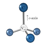
The four dangling sp3 orbitals at the VSi site contribute four electrons. If VSi captures an additional electron, it becomes a negatively charged silicon vacancy (V) Baranov et al. (2013); Soykal et al. (2016); Anisimov et al. (2018); Wagner et al. (2002) whose spin state was shown to be = 3/2 by a radiofrequency-optical double resonance technique Riedel et al. (2012); Soykal et al. (2016). The site symmetry of V is C3v, as shown in Fig. 1. Several separately addressable V have been identified in the same crystal for each of the main SiC polytypes: hexagonal 4H-SiC and 6H-SiC and rhombic 15R-SiC. The 4H-SiC polytype, e.g., hosts one hexagonal () and one cubic () lattice site and in 6H-SiC there are one hexagonal and two cubic sites (, and ). V at a hexagonal site of 4H- and 6H-SiC is called a V2 type vacancy, at a cubic site of 4H-SiC it is called V1 and in 6H-SiC V1 and V3 are located at sites and Sörman et al. (2000).
The spins of V in SiC are highly controllable and can be manipulated with the techniques that have been developed, e.g., for working with diamond NV qubits. This was demonstrated with ensembles Koehl et al. (2011) as well as with single centers Widmann et al. (2014). Optically induced spin polarisation of the ground state at room temperature has been demonstrated using electron spin resonance Soltamov et al. (2012). This spin polarisation can be used to implement solid-state masers and extraordinarily sensitive radio-frequency amplifiers Kraus et al. (2013) or magnetic field sensors with dc field sensitivities Simin et al. (2016). In some V the zero-field splitting (ZFS) is nearly temperature independent, making these centers very attractive for vector magnetometry. Contrarily, the zero-field splitting of the centers V2 centers in 4H-SiC in the excited state exhibits a large thermal shift, which makes them useful for thermometry applications Anisimov et al. (2016). All four ground state spin levels of V have been used to demonstrate absolute dc magnetometry, which is immune to thermal noise and strain inhomogeneity Soltamov et al. (2019).
I.2 Preserving spin coherence
An important precondition for the implementation of quantum technologies, including quantum information processing is that the phase of superposition states can be preserved for times significantly longer than the duration of the computational task DiVincenzo (2000); Stolze and Suter (2008). Achieving this goal generally requires an array of measures Suter and Álvarez (2016), including passive schemes like decoherence-free subspaces Lidar et al. (1998) or active schemes like spin-echoes Hahn (1950). In divacancy spin ensembles in 4H-SiC, Hahn-echo times longer than 1 ms were observed at 20 K Christle et al. (2014).
In most cases, the interactions with the environment that cause the dephasing are not static and a single refocusing pulse is not sufficient to completely suppress the dephasing. For those cases, multiple echo sequence were developed by Carr and Purcell Carr and Purcell (1954), consisting of equidistant pulses. This basic experiment was improved to make it more robust with respect to experimental imperfections Meiboom and Gill (1958); Souza et al. (2011, 2012). These so-called dynamical decoupling (DD) techniques have been applied to extend the coherence times of different types of qubits, including, e.g., rare-earth ions Zhong et al. (2015) and the spin of the NV center in diamonds Shim et al. (2012). In the V2 vacancy of the 4H-SiC polytype, the efficiency of the spin-echo experiment depends strongly on the magnetic field Carter et al. (2015). Combining Carr-Purcell-Meiboom-Gill (CPMG) decoupling with a static magnetic field can extend the spin coherence time of the V2 center in 4H-SiC to more than 20 ms Simin et al. (2017).
I.3 Outline of this paper
In this work, we focus on the 6H-SiC polytype whose spin properties have not yet been studied in detail. Sec. II gives details of the sample preparation, photoluminescence measurement, and the optical pumping scheme. Sec. III describes the experimental setup for continuous-wave as well as pulsed optically detected magnetic resonance (ODMR) measurements. Sec. IV describes the results of the spin-lattice and spin-spin relaxation measurements. Sec. V contains the discussion and concluding remarks.
II System
II.1 Sample
The experiments were performed on a sample that was isotopically enriched in 28Si and 13C. The Si enrichment was performed using gas-centrifuge technology, resulting in an isotopic purity of 99.999%, which was available in the form of small 28Si pieces (1-3 mm). The 13C source was carbon powder enriched to 15% in 13C. The SiC crystal was grown at a temperature of 2300°-2400°C on a (0001) Si face in an Argon atmosphere at a growth rate of 100m/h. After growing the SiC crystal, machining and cutting of the wafers were carried out. The isotope composition was measured by Secondary Ion Mass Spectroscopy(SIMS). The concentrations of 28Si, 29Si, and 30Si are 99.918 %, 0.076%, and 0.006 %, respectively. The concentrations of 12C and 13C are 95.3% and 4.7%, respectively. To create V centers, the crystal was irradiated with electrons with a dose of 1018cm-2 and an energy of 2 MeV at room temperature.
II.2 Photoluminescence
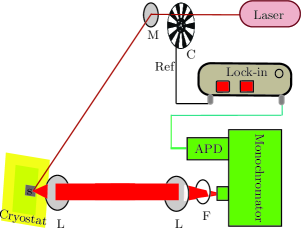
To measure the Photoluminescence (PL) of the sample, we used the setup shown schematically in Fig. 2. A Ti:sapphire laser provided the optical excitation. The PL was collected with the help of two convex lenses of focal length 20 cm. The PL was collected in the direction of the -axis and passed through a long-pass 850 nm filter (F; Thorlabs) to a monochromator (Spex 1704). An avalanche photodiode (APD) module with a frequency bandwidth from DC to 100 kHz (C5460-1 series from Hamamatsu) was attached to the monochromator for detecting the PL. The voltage output of this APD was measured with the lock-in amplifier (SRS model SR830). The laser beam was modulated with a chopper, whose sync signal served as reference for the lock-in amplifier.
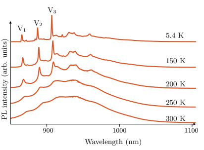
Fig. 3 shows some PL spectra recorded at different temperatures with the excitation laser set to 790 nm. The sample was cooled down using a Helium cryostat, and the PL spectra recorded at 5.4 K, 150 K, 200 K, 250 K and 300 K are shown. The zero phonon lines (ZPL) of the negatively charged vacancies are visible at the expected wavelengths of 865 nm (V1), 887 nm (V2) and 908 nm (V3) Sörman et al. (2000); Wagner et al. (2000).
II.3 Energy levels and optical pumping
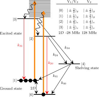
The negatively charged defects in 6H-SiC have spin = 3/2 Riedel et al. (2012); Soykal et al. (2016). Fig. 4 shows the energy-level diagram of the 6H-SiC V in the absence of an external magnetic field. The states and in the electronic ground state correspond to the and spin states. In the absence of a magnetic field, they form two degenerate doublets, which are split by the zero-field interaction. In the case of the V1/V3 vacancy, the are lower in energy, i.e. they correspond to state , in the vacancy, the states are the lowest energy states Kraus et al. (2013); Biktagirov et al. (2018). The states and represent the , ( ) and () spin substates of the electronically excited states of V1/V3 (V2) Baranov et al. (2011); Fuchs et al. (2015). The shelving state is an state, which is important for the optical pumping process Baranov et al. (2011).
The spin Hamiltonian of the states is
| (1) |
where the zero field splitting in the electronic ground state is MHz for V1/V3 and 128 MHz for V2 Biktagirov et al. (2018), is the electron -factor, is the Bohr magneton, is the external magnetic field, is the vector of the electron spin operators. We use a coordinate system whose -axis is oriented along the C3 symmetry axis, which is also the -axis. In the absence of optical pumping, when the spin system is in thermal equilibrium at room temperature, all four ground states are almost equally populated. When the system is irradiated with a laser, the populations are re-distributed, as shown schematically in Fig. 4. When the laser is turned on, it excites transitions from the ground states and to the excited states and . From the excited states and most of the population falls back to the and states by spontaneous emission with a rate and . However, the system can also undergo intersystem-crossing (ISC) to the shelving states with the rates and Baranov et al. (2011). From there the system returns to the ground state, with a bias for the state over state with the rates and Riedel et al. (2012); Biktagirov et al. (2018); Soltamov et al. (2019). The exact ISC rates from and to the shelving state are not yet known precisely but, by considering the recorded ODMR data shown in Fig. 5, 34 > 24 for V1/V3 and > for V2.
III Optically detected magnetic resonance
III.1 Continuous-wave ODMR
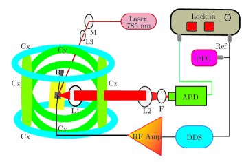
To determine the ground state spin Hamiltonian of the V in the sample, we used the continuous-wave (cw) ODMR technique with the setup shown in Fig. 6. Our light source was a 785 nm laser diode with a maximum power of 400 mW, which was driven by a Thorlabs laser diode controller (LDC202C series) with a thermoelectric temperature controller (TED 200C). We used three orthogonal Helmholtz coil-pairs for applying the static magnetic field in an arbitrary direction. A highly stable linear current source (Servowatt, three-channel DCP-390/30) delivers currents up to 15A to the coils. The currents were controlled individually by an analog control voltage. The radio-frequency (RF) signal was generated with a direct digital synthesizer (DDS) AD9915 from Analog Devices which generates signals up to 1 GHz. Its output was amplified using an RF amplifier (Mini- Circuit LZY-1, 50W amplifier with a frequency range from 20 MHz to 512 MHz) and sent to a 50 m wire terminated with a 50 resistor. A programmable function generator (PFG, Hameg model HM8130-2) was used to modulate the amplitude of the RF field. A laser beam was focused on the sample using a convex lens (L3) of focal length 20 cm. The PL from the sample was collected with a pair of lenses (L1 and L2 with focal lengths 5 cm and 15 cm respectively), sent through a 850 nm long-pass filter to suppress stray light from the laser and to an avalanche photodiode (APD) module with a frequency range from DC to 10 MHz (C12703 series from Hamamatsu). The APD signal was demodulated with a lock-in amplifier (SRS model SR830 DSP) whose reference signal was derived from the PFG modulating the RF.
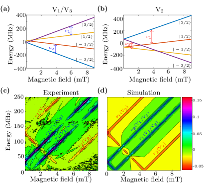
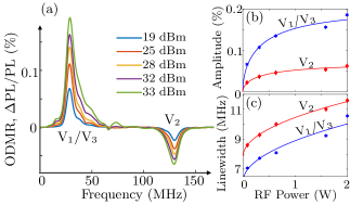
Fig. 5(a) shows the ODMR signal recorded in the absence of a magnetic field by sweeping the frequency of the RF at different RF powers, using the setup shown in Fig. 6. Two peaks with different signs are observed: a positive one (i.e. increase of PL at the application of RF) at 28 MHz and a negative one at 128 MHz. In a previous work Sörman et al. (2000), it was shown that the peak at 128 MHz corresponds to the V at lattice sites ( type) and the peak at 28 MHz corresponds to V at two quasi-cubic sites and (V1 and V3 type) which have the same value Sörman et al. (2000). Recently it has been shown the peak at 28 MHz corresponds to V at quasi-cubic site and the peak at 128 MHz corresponds to the V at the quasi-cubic site (V3 type) Biktagirov et al. (2018). Since the ODMR peaks assignment is still debatable, we will follow the ODMR peaks assignment used in earlier work Sörman et al. (2000).
The overall ODMR contrast is relatively small, but comparable to the values from similar systems (see, e.g.,Soltamov et al. (2019); Simin et al. (2017); Kraus et al. (2013); Anisimov et al. (2016)). While not all the relevant parameters are known, one reason for the relatively small contrast is that the PL from the different types of vacancies can not be separated at room temperature, as shown in Fig. 3. The measured PL therefore includes baseline contributions from other centers that do not depend on the magnetic resonance.
The variation of amplitude and linewidth with RF power is shown in Fig. 5 (b) and (c), respectively. The amplitude data were fitted with the function
where is the signal amplitude and the RF power. and are the fitting parameters and the resulting values were 0.2087 and 0.8573 (0.07112 and 0.8834 ) for V1/ V3 (V2) respectively. The linewidth data were fitted to the function
where is the linewidth. The resulting values for the fitting parameters and were 6.193 MHz and 2.713 MHz W-1/2 (7.877 MHz and 2.579 MHz W-1/2) for V1/V3 (V2) respectively. At the maximum RF power that we could apply, 33 dBm, the ODMR signal reached an amplitude of 0.19 % (-0.06 %) for V1/V3 (V2) and the linewidth of V1/V3 (V2) was 10.24 MHz (11.70 MHz).
Figures 7 (a) and (b) shows the energy levels of V1/V3 and V2 as a function of the magnetic field applied -axis, calculated from the Hamiltonian given in Eq. (1). Arrows labeled with and represent the transition from and respectively. Fig. 7 (c) summarises the ODMR spectra for a range of magnetic fields from 0 to 9 mT, applied parallel to the -axis, using an RF power of 32 dBm (1.6 W). In this plot the magnetic field strength is plotted along the horizontal axis and the vertical axis corresponds to the RF frequency. The relative change of the PL is color-coded as shown by the color bar to the right of the plot. For frequencies < 20 MHz, the RF power generated by the available amplifier drops significantly, which leads to the very small ODMR signal in this range. Also, at a frequency of 165 MHz, we observed very small signals , which appears to be do to a standing wave in our RF system, which was not impedance-matched to the 50 amplifier. The experimental data compare well to the superposition of the signals from the two types of Si vacancies, which is shown in Fig. 7 (d). For this simulation, the transition frequencies are obtained from the Hamiltonian of Eq. (1), while amplitudes and linewidths are taken from the experimental data.
III.2 Pulsed ODMR
The uncontrolled interaction with a noisy environment has two effects on a system that has been excited from its thermal equilibrium state: it causes dephasing and a return of the system to the thermal equilibrium state. If the system is used in quantum technology applications Nielsen and Chuang (2000); Stolze and Suter (2008), both effects are unwanted since long coherence times are an essential requirement for technologies like quantum computing, quantum metrology and quantum memories. To assess the suitability of for these applications, a precise characterisation of the decoherence processes is therefore essential. For this purpose, we use the time-resolved ODMR technique Depinna and Cavenett (1982); Langof et al. (2002).
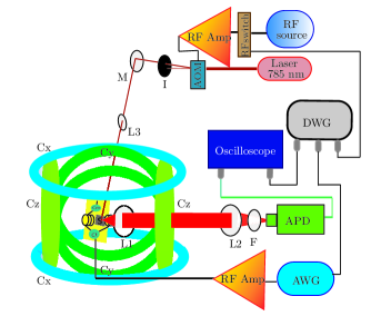
For the time-resolved measurements, we modified the setup of Fig. 6 to generate laser- and RF pulses of variable duration. Fig. 8 shows the modified setup. For generating the laser pulses, we used an acousto-optical modulator (AOM; NEC model OD8813A). The center frequency of the AOM was 100 MHz, and the RF power was 1.2 W. The RF control signal was generated by a programmable 1 GHz synthesizer HM8133-2 and the RF pulses were generated by an RF switch (Mini-Circuits ZASWA-2-50DR+, DC-5 GHz). The TTL pulses that control the timing were generated by a SpinCore PulseBlaster ESR-PRO PCI card. The RF pulses that drive the spins were generated by an AWG (WavePond - Chase Scientific, DAx14000). The RF pulses were amplified up to 50 W and applied to the SiC sample through a tuned circuit for minimizing reflections. The signal from the APD detector was recorded with a USB card (PicoScope 2000 series) attached to a computer.
In all experiments described below, a laser pulse of 75 mW power and 300 s duration initializes the SiC vacancies by populating the state more than the state . At this laser intensity, the time constant for the transfer of population to spin state is 28 s (11 s) for V2 (V1/V3). After the polarisation of the spin system, a sequence of RF pulses was applied to the system, as discussed in detail below. To read out the final state of the spin system, we applied a second laser pulse of duration 4 s during which we collect the PL as described in Sec. IIIA. In the time-resolved experiment, we averaged the signal 500 times and subtracted it from a 500 times averaged signal of a reference pulse sequence to remove unwanted background signals. This process was repeated 5 times and again the average was taken .
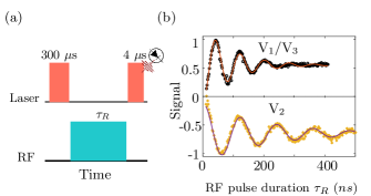
To calibrate the strength of the RF field for the pulsed excitation, we performed a measurement of Rabi oscillations for the transition between the and of , using the pulse sequence shown in Fig. 9 (a). After this initializing laser pulse, a 16 W RF pulse of variable duration was applied. Here the reference signal was obtained from an experiment without an RF pulse. Fig. 9 (b), shows the resulting experimental data for the V1/ V3 and V2 type vacancies. The experimental data were fitted to the function
| (2) |
where SRF() is the signal measured with an the RF pulse of duration and S0() the reference signal without RF pulse. For V1/V3, we obtained the fit parameters = , = , = , = MHz, = ns and for V2 = , = , = = MHz, = ns.
IV Relaxation measurements
IV.1 Population relaxation
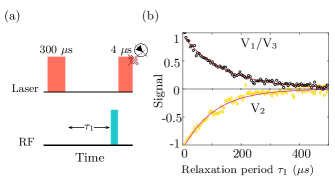
Spin-lattice relaxation is the process by which the populations of the spin system relax to the thermal equilibrium state. It is also known as longitudinal relaxation and contributes to the decoherence process. The pulse sequence used to measure the longitudinal relaxation is shown in Fig.10 (a). After the initializing laser pulse the system was allowed to relax for a time and then the measuring laser pulse was applied to record the remaining population difference. The result of this experiment was subtracted from a similar experiment where the populations of the levels and were inverted by a pulse applied to the transition between them. Fig.10 (b) shows the resulting signals for both vacancy spins as a function of the delay . The experimental signal was fitted to the function
where and are the average signal measured during the reference and the main pulse sequence respectively for different delays . From the fit, we obtained the relaxation times 142.13.6 s and 1076.6 s for the V1/V3 and V2 sites, respectively.
IV.2 Free Induction Decay
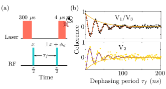
Another important process is the decay of coherence, which can be observed in a free induction decay (FID) measurement. While the free precession of spin coherence can be observed directly in conventional magnetic resonance, here we used the Ramsey scheme Ramsey (1950) where a RF pulse converted the coherence into a population difference, which was then read out during the final laser pulse. Figure 11 shows the experimental scheme: After the initialisation by the first laser pulse, the first RF pulse generated the coherence, which was then allowed to precess for a time before it was read out. We again used the difference between two experiments, where the two RF pulses have a phase difference of and , respectively, to suppress unwanted background signals. Fig. 11 (b), shows the FIDs measured with a detuning frequency of =40 MHz, together with a fit to the a function
| (3) |
where and are the average PL signals measured with the detection pulse. The fit parameter =38 ns for V1/V3 and =31 ns for V2 at room temperature and in the absence of an external magnetic field.
IV.3 Spin-echo
The decay of the coherence is due to different types of interactions that are broadly classified as homogeneous vs. inhomogeneous. They can be separated by the spin-echo experiment (Hahn-echo) Hahn (1950). We will refer to the homogenous decay time of the Hahn echo as .
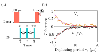
Fig. 12 (a) shows the pulse sequence for measuring the spin-echo relaxation. After the initializing laser-pulse, we applied a RF pulse, which created the coherence that evolved freely for a time . We then applied a refocusing pulse, and a second delay. The remaining coherence was converted into population by the third RF pulse and read out during the final laser pulse. In this sequence, all RF pulses were applied along the -axis. In the reference signal, the last pulse was applied along the --axis, which changed the sign of the resulting population difference. Subtracting the signals from the two experiments thus yielded a background-free measurement of the coherence. Fig.12 (b), plots the resulting data as a function of the dephasing period , together with a fit to an exponential decay
where and are the signals measured with the pulse. The resulting values for were s and s for the V1/V3 and V2 centers at room temperature and in the absence of an external magnetic field.
IV.4 Echo trains
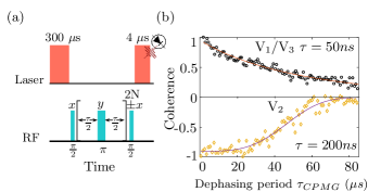
Multiple refocusing pulses can extend the lifetime of the coherence further, compared to the case of a single echo, if the perturbation is not static, but its correlation time is longer than the spacing between the echo pulses Carr and Purcell (1954); Meiboom and Gill (1958); Suter and Álvarez (2016). We therefore measured the coherence time of the centers during a CPMG pulse sequence, as shown in Fig. 13 (a). After the initializing laser-pulse, the RF pulse created spin coherence. During the subsequent delay, we applied refocusing pulses, each with flip angle . The final pulse converted the coherence back into population which was read out as discussed above. To eliminate background signals, we subtracted the results of the two experiments where the final RF pulse rotated the spins around the axes. The difference between the experimentally observed signals was fitted to the function
| (4) |
where the total evolution period is =, is number of pulses and is the duration of a pulse, which was ns for V1/ V3 and ns for V2. Fig. 13 (b) shows the experimental data for a pulse spacing of ns for V1/V3 and ns for V2 . The fitted parameters are = s, for V1/V3 and = s, = 3.47 for V2 at room temperature and in the absence of an external magnetic field.
V Discussion and Conclusion
V centers in SiC have interesting properties that may become useful in future quantum devices, similar to the NV center in diamond. In this work, we have studied in detail their properties in the 6H-SiC polytype. We studied the photoluminescence spectrum as a function of temperature. At low temperature, the ZPLs of the V1, V2 and V3 are quite sharp but broaden with increasing temperature.
These V centers can be spin-polarised by optical irradiation, the spin can be manipulated by RF fields and read out optically . In zero field, the ODMR spectrum shows two peaks with opposite amplitudes, one at 28 MHz and the other at 128 MHz. They can be assigned to the V1/ V3 and V2 type V Sörman et al. (2000). ODMR transitions as a function of the magnetic field parallel to -axis were measured for both V.
The main emphasis of this work was on the coherence properties of the spins during free precession as well as during the application of refocusing sequences designed to protect the spins against environmental noise. Using a train of echo pulses, we could extend the coherence time of the V in the 6H-SiC polytype at room temperature up to 50 s. Previous experimental room temperature studies on V2 type vacancy in 4H-SiC in the absence of external magnetic field reported free evolution time and spin-echo decay times of 190-300 ns and 6-8 us respectively Carter et al. (2015); Simin et al. (2017). The isotopic composition of the 4H-SiC samples used in those studies was natural abundance, i.e. with 4.7 % of 29Si and 1.1 % of 13C, both of which have nuclear spins . Since the atoms closest to the Si vacancy are all 13C nuclei, their hyperfine interaction is approximately an order of magnitude stronger than that of the 29Si nuclei located in the next-nearest neighbor (NNN) shell consisting of twelve silicon atoms Wagner et al. (2002); Yang et al. (2014); Witzel et al. (2005). The decoherence of the vacancy-spin ensemble is mainly due to dipolar fluctuations of the nuclear spins Witzel et al. (2005); Yang et al. (2014) which couple to the electron spin couples by hyperfine interaction Yang et al. (2014). A higher percentage of 13C therefore reduces the coherence time. We expect that the coherence times can be extended by applying suitable magnetic fields and dynamical decoupling schemes Carter et al. (2015); Simin et al. (2017). Lowering the temperature will also extend the spin-lattice relaxation time Simin et al. (2017). These possibilities will be explored in upcoming work.
Acknowledgements.
This work was supported by the Deutsche Forschungsgemeinschaft in the frame of the ICRC TRR 160 (Project No. C7)and by RFBR, project number 19-52-12058. SIMS measurements were performed using the Center of Multi-User Equipment “Material Science and Diagnostics for Advanced Technologies” (Ioffe Institute, Russia) facility supported by the Russian Ministry of Science (The Agreement ID RFMEFI62119X0021).References
- Tarasenko et al. (2018) S. A. Tarasenko, A. V. Poshakinskiy, D. Simin, V. A. Soltamov, E. N. Mokhov, P. G. Baranov, V. Dyakonov, and G. V. Astakhov, physica status solidi (b) 255, 1870101 (2018).
- Falk et al. (2013) A. L. Falk, B. B. Buckley, G. Calusine, W. F. Koehl, V. V. Dobrovitski, A. Politi, C. A. Zorman, P. X.-L. Feng, and D. D. Awschalom, Nat. Commun. 4, 1819 (2013).
- Janzén et al. (2009) E. Janzén, A. Gali, P. Carlsson, A. Ga§llstrom, B. Magnusson, and N. Son, Physica B: Condensed Matter 404, 4354 (2009).
- Maboudian et al. (2013) R. Maboudian, C. Carraro, D. G. Senesky, and C. S. Roper, Journal of Vacuum Science & Technology A 31, 050805 (2013).
- Song et al. (2011) B.-S. Song, S. Yamada, T. Asano, and S. Noda, Opt. Express 19, 11084 (2011).
- Wang et al. (2017) J. Wang, Y. Zhou, X. Zhang, F. Liu, Y. Li, K. Li, Z. Liu, G. Wang, and W. Gao, Phys. Rev. Applied 7, 064021 (2017).
- Widmann et al. (2014) M. Widmann, S.-Y. Lee, T. Rendler, N. T. Son, H. Fedder, S. Paik, L.-P. Yang, N. Zhao, S. Yang, I. Booker, A. Denisenko, M. Jamali, S. A. Momenzadeh, I. Gerhardt, T. Ohshima, A. Gali, E. Janzén, and J. Wrachtrup, Nature Materials 14, 164 (2014).
- Baranov et al. (2005) P. G. Baranov, I. V. Il’in, E. N. Mokhov, M. V. Muzafarova, S. B. Orlinskii, and J. Schmidt, Journal of Experimental and Theoretical Physics Letters 82, 441 (2005).
- Son et al. (1999) N. T. Son, P. N. Hai, M. Wagner, W. M. Chen, A. Ellison, C. Hallin, B. Monemar, and E. Janzén, Semiconductor Science and Technology 14, 1141 (1999).
- Kraus et al. (2013) H. Kraus, V. A. Soltamov, D. Riedel, S. Väth, F. Fuchs, A. Sperlich, P. G. Baranov, V. Dyakonov, and G. V. Astakhov, Nature Physics 10, 157 (2013).
- Baranov et al. (2011) P. G. Baranov, A. P. Bundakova, A. A. Soltamova, S. B. Orlinskii, I. V. Borovykh, R. Zondervan, R. Verberk, and J. Schmidt, Phys. Rev. B 83, 125203 (2011).
- Fuchs et al. (2015) F. Fuchs, B. Stender, M. Trupke, D. Simin, J. Pflaum, V. Dyakonov, and G. V. Astakhov, Nature Communications 6, 7578 (2015).
- Sörman et al. (2000) E. Sörman, N. T. Son, W. M. Chen, O. Kordina, C. Hallin, and E. Janzén, Phys. Rev. B 61, 2613 (2000).
- Mizuochi et al. (2002) N. Mizuochi, S. Yamasaki, H. Takizawa, N. Morishita, T. Ohshima, H. Itoh, and J. Isoya, Phys. Rev. B 66, 235202 (2002).
- von Bardeleben et al. (2000) H. J. von Bardeleben, J. L. Cantin, I. Vickridge, and G. Battistig, Phys. Rev. B 62, 10126 (2000).
- Wagner et al. (2002) M. Wagner, N. Q. Thinh, N. T. Son, W. M. Chen, E. Janzén, P. G. Baranov, E. N. Mokhov, C. Hallin, and J. L. Lindström, Phys. Rev. B 66, 155214 (2002).
- Carlos et al. (2006) W. E. Carlos, N. Y. Garces, E. R. Glaser, and M. A. Fanton, Phys. Rev. B 74, 235201 (2006).
- Orlinski et al. (2003) S. B. Orlinski, J. Schmidt, E. N. Mokhov, and P. G. Baranov, Phys. Rev. B 67, 125207 (2003).
- Son et al. (2006) N. T. Son, P. Carlsson, J. ul Hassan, E. Janzén, T. Umeda, J. Isoya, A. Gali, M. Bockstedte, N. Morishita, T. Ohshima, and H. Itoh, Phys. Rev. Lett. 96, 055501 (2006).
- Christle et al. (2014) D. J. Christle, A. L. Falk, P. Andrich, P. V. Klimov, J. U. Hassan, N. Son, E. Janzén, T. Ohshima, and D. D. Awschalom, Nature Materials 14, 160 (2014).
- Lingner et al. (2001) T. Lingner, S. Greulich-Weber, J.-M. Spaeth, U. Gerstmann, E. Rauls, Z. Hajnal, T. Frauenheim, and H. Overhof, Phys. Rev. B 64, 245212 (2001).
- Baranov et al. (2013) P. Baranov, V. A. Soltamov, A. A. Soltamova, G. V. Astakhov, and V. D. Dyakonov, in Silicon Carbide and Related Materials 2012, Materials Science Forum, Vol. 740 (Trans Tech Publications Ltd, Bäch Switzerland, 2013) pp. 425–430.
- Soykal et al. (2016) O. O. Soykal, P. Dev, and S. E. Economou, Phys. Rev. B 93, 081207(R) (2016).
- Anisimov et al. (2018) A. N. Anisimov, V. A. Soltamov, I. D. Breev, R. A. Babunts, E. N. Mokhov, G. V. Astakhov, V. Dyakonov, D. R. Yakovlev, D. Suter, and P. G. Baranov, AIP Advances 8, 085304 (2018).
- Riedel et al. (2012) D. Riedel, F. Fuchs, H. Kraus, S. Väth, A. Sperlich, V. Dyakonov, A. A. Soltamova, P. G. Baranov, V. A. Ilyin, and G. V. Astakhov, Phys. Rev. Lett. 109, 226402 (2012).
- Koehl et al. (2011) W. F. Koehl, B. B. Buckley, F. J. Heremans, G. Calusine, and D. D. Awschalom, Nature 479, 85 (2011).
- Soltamov et al. (2012) V. A. Soltamov, A. A. Soltamova, P. G. Baranov, and I. I. Proskuryakov, Phys. Rev. Lett. 108, 226402 (2012).
- Simin et al. (2016) D. Simin, V. A. Soltamov, A. V. Poshakinskiy, A. N. Anisimov, R. A. Babunts, D. O. Tolmachev, E. N. Mokhov, M. Trupke, S. A. Tarasenko, A. Sperlich, P. G. Baranov, V. Dyakonov, and G. V. Astakhov, Phys. Rev. X 6, 031014 (2016).
- Anisimov et al. (2016) A. N. Anisimov, D. Simin, V. A. Soltamov, S. P. Lebedev, P. G. Baranov, G. V. Astakhov, and V. Dyakonov, Scientific Reports 6, 33301 (2016).
- Soltamov et al. (2019) V. A. Soltamov, C. Kasper, A. V. Poshakinskiy, A. N. Anisimov, E. N. Mokhov, A. Sperlich, S. A. Tarasenko, P. G. Baranov, G. V. Astakhov, and V. Dyakonov, Nature Communications 10, 1678 (2019).
- DiVincenzo (2000) D. P. DiVincenzo, Fortschritte der Physik 48, 771 (2000).
- Stolze and Suter (2008) J. Stolze and D. Suter, Quantum Computing: A Short Course from Theory to Experiment, 2nd ed. (Wiley-VCH, Berlin, 2008).
- Suter and Álvarez (2016) D. Suter and G. A. Álvarez, Rev. Mod. Phys. 88, 041001 (2016).
- Lidar et al. (1998) D. A. Lidar, I. L. Chuang, and K. B. Whaley, Phys. Rev. Lett. 81, 2594 (1998).
- Hahn (1950) E. Hahn, Phys. Rev. 80, 580 (1950).
- Carr and Purcell (1954) H. Y. Carr and E. M. Purcell, Phys. Rev. 94, 630 (1954).
- Meiboom and Gill (1958) S. Meiboom and D. Gill, Review of Scientific Instruments 29, 688 (1958).
- Souza et al. (2011) A. M. Souza, G. A. Álvarez, and D. Suter, Phys. Rev. Lett. 106, 240501 (2011).
- Souza et al. (2012) A. M. Souza, G. A. Álvarez, and D. Suter, Philosophical Transactions of the Royal Society A: Mathematical, Physical and Engineering Sciences 370, 4748 (2012).
- Zhong et al. (2015) M. Zhong, M. P. Hedges, R. L. Ahlefeldt, J. G. Bartholomew, S. E. Beavan, S. M. Wittig, J. J. Longdell, and M. J. Sellars, Nature 517, 177 (2015).
- Shim et al. (2012) J. H. Shim, I. Niemeyer, J. Zhang, and D. Suter, EPL (Europhysics Letters) 99, 40004 (2012).
- Carter et al. (2015) S. G. Carter, O. O. Soykal, P. Dev, S. E. Economou, and E. R. Glaser, Phys. Rev. B 92, 161202(R) (2015).
- Simin et al. (2017) D. Simin, H. Kraus, A. Sperlich, T. Ohshima, G. V. Astakhov, and V. Dyakonov, Phys. Rev. B 95, 161201(R) (2017).
- Wagner et al. (2000) M. Wagner, B. Magnusson, W. M. Chen, E. Janzén, E. Sörman, C. Hallin, and J. L. Lindström, Phys. Rev. B 62, 16555 (2000).
- Biktagirov et al. (2018) T. Biktagirov, W. G. Schmidt, U. Gerstmann, B. Yavkin, S. Orlinskii, P. Baranov, V. Dyakonov, and V. Soltamov, Phys. Rev. B 98, 195204 (2018).
- Nielsen and Chuang (2000) M. A. Nielsen and I. L. Chuang, Quantum Computation and Quantum Information (Cambridge University Press, Cambridge UK, 2000).
- Depinna and Cavenett (1982) S. P. Depinna and B. C. Cavenett, Journal of Physics C: Solid State Physics 15, L489 (1982).
- Langof et al. (2002) L. Langof, E. Ehrenfreund, E. Lifshitz, O. I. Micic, and A. J. Nozik, The Journal of Physical Chemistry B 106, 1606 (2002).
- Ramsey (1950) N. F. Ramsey, Phys. Rev. 78, 695 (1950).
- Yang et al. (2014) L.-P. Yang, C. Burk, M. Widmann, S.-Y. Lee, J. Wrachtrup, and N. Zhao, Phys. Rev. B 90, 241203(R) (2014).
- Witzel et al. (2005) W. M. Witzel, R. de Sousa, and S. Das Sarma, Phys. Rev. B 72, 161306(R) (2005).