Impact of Substrate on Tip-enhanced Raman Spectroscopy — A Comparison of Frequency Domain Simulations and Graphene Measurements
Abstract
Tip-enhanced Raman spectroscopy (TERS) has reached nanometer spatial resolution for measurements performed at ambient conditions and sub-nanometer resolution at ultra high vacuum. Super-resolution (beyond the tip apex diameter) TERS has been obtained, mostly in the gap mode configuration, where a conductive substrate localizes the electric fields. Here we present experimental and theoretical TERS to explore the field distribution responsible for spectral enhancement. We use gold tips of apex diameter to measure TERS on graphene, a spatially delocalized two-dimensional sample, sitting on different substrates: (i) glass, (ii) a thin layer of gold and (iii) a surface covered with diameter gold spheres, for which resolution is achieved at ambient conditions. The super-resolution is due to the field configuration resulting from the coupled tip-sample-substrate system, exhibiting a non-trivial spatial surface distribution. The field distribution and the symmetry selection rules are different for non-gap vs. gap mode configurations. This influences the overall enhancement which depends on the Raman mode symmetry and substrate structure.
I Introduction
Tip-enhanced Raman spectroscopy (TERS) is an optical imaging technique with a resolution far beyond the diffraction limit of light, which provides, simultaneously, scanning probe microscopy (SPM) and Raman spectroscopy information Wessel (1985); Stöckle et al. (2000); Hartschuh et al. (2003a, b); Hagen et al. (2005); Maciel et al. (2008); Bailo and Deckert (2008); Cançado et al. (2009); Yeo et al. (2009); Yano et al. (2009); Van Schrojenstein Lantman et al. (2012); Kumar et al. (2015); Park et al. (2016); Wang et al. (2017); Beams (2018). It is based on the illumination of a sharp metallic tip that, on one hand, concentrates the incoming exciting electromagnetic field to a nanoscale near-field at the tip apex and, on the other hand, collects the near-field Raman scattering from the sample, resulting in a localized and enhanced stimulation of the sample’s scattering Yang et al. (2009a); Deckert (2009); Shi et al. (2017). Therefore, it is not uncommon to simplistically assume that the TERS characteristics, including imaging resolution, is defined solely by the tip apex structure. However, several TERS experiments have now shown resolutions far beyond the tip apex dimension, achieving the nanometer scale in air Chen et al. (2014) and the angstrom scale in ultra-high vacuum Zhang et al. (2013a); Lee et al. (2019); Baumberg et al. (2019). Such “super-resolution” has been obtained using unexpected tricks, like local tip-induced pressure Yano et al. (2009), and in most cases utilizing the so-called gap mode configuration, where the enhancement can be further increased by locating the sample between the tip and a flat metallic substrate Zhang et al. (2007); Stadler et al. (2013); Zhang et al. (2013b). Whereas in the conventional TERS configuration the field enhancement at the tip apex is conventionally due to the excitation of localized surface plasmon resonance on the tip shaft Vasconcelos et al. (2015, 2018), the gap mode configuration makes use of the electric field enhancement by the gap-plasmon resonance that appears in the confined dielectric space between the tip end and the metallic substrate Becker et al. (2016).
In this work, we study the spatial distribution of the field enhancement during TERS experiments in three different TERS configurations: regular (non-gap mode), gap mode with a continuous metallic substrate, and a “structured” gap mode, utilizing regularly spaced metallic nanospheres as substrate. As a reference sample we utilize graphene, a strong and two-dimensional Raman scatterer Jorio et al. (2011, 2019), which enables total surface sensing on top of the different substrates to show the significant influence of the substrate structure in the TERS results. We first introduce, in Section II, the technical aspects. In Section III the experimental results are discussed, separated in three main findings: (A) TERS efficiency as a function of the tip-laser alignment within the focus; (B) TERS enhancement dependence on substrate structure and phonon symmetry; (C) the achievement of super-resolution for “structured” gap mode. We then focus, in Section IV, on how the “structured” gap mode is capable of generating an apparent super-resolution image. In Section V we present the conclusions of this work.
II Technical Aspects
II.1 Experimental Setup
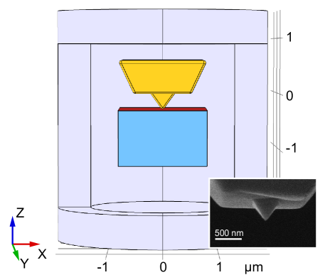
The TERS system consists of a combination of a non-contact atomic force microscope (AFM) and a micro-Raman spectrometer, optimized for a high numerical aperture (NA = 1.4) optical excitation and collection on a backscatter configuration Cançado et al. (2009). The AFM setup is a home-made shear-force system with a tuning fork operating at , associated with a Phase-Locked Loop system that controls the tip-sample distance. Considering that the TERS setup is based on a radially polarized He-Ne laser beam with a 632.8 nm wavelength, a resonant gold pyramidal tip, denominated Plasmon-Tuned Tip Pyramid (PTTP), was used (see inset to Fig. 1) Vasconcelos et al. (2018). This tip is capable of holding localized surface plasmon resonance, in this case tuned for the given excitation wavelength. In addition, the tip used has a apex diameter, as measured by Scanning Electron Microscopy (SEM).
II.2 Sample Preparation
Graphene, as a spatially delocalized two-dimensional TERS sample, was prepared by the mechanical exfoliation method and deposited on three different substrates: (i) glass; (ii) a thick layer of gold evaporated on glass (Au film); (iii) a surface of diameter oleylamine-stabilized gold nanoparticles (AuNP) with an edge-to-edge inter-particle separation of between the particle surfaces in a roughly hexagonal lattice Schulz et al. (2017); Mueller et al. (2018).
II.3 Group Theory Analysis
Considering graphene pertains to the point group, the G band, observed at cm-1 belongs to the irreducible representation, while the second-order 2D band (also known as G’ band), observed at cm-1) is a totally symmetric mode. The Raman tensors for the G and 2D bands of graphene, considering the presence of a highly focused field Budde et al. (2016), are given by:
| (1) |
and
| (2) |
From symmetry, the G band can only be activated by electric fields in the graphene (XY) plane. The 2D band can also be activated by fields polarized perpendicular to the graphene plane (Z). The value is not known in the literature, but experiments Budde et al. (2016) indicate that .
The selection rules for TERS have been derived by group theory Jorio et al. (2017). The phonon active modes for the different scattering processes are defined by:
| (3a) | |||
| (3b) | |||
| (3c) | |||
| (3d) | |||
where S is the usual Raman scattering Stokes process, where light interacts only with the sample; SP and PS are processes where the interaction of the incoming and outgoing light, respectively, is mediated by the plasmonic structure; PSP is a process where both incoming and outgoing light interactions are mediated by the plasmon. Notice Equation (3c) is different from what has been presented in Ref.Jorio et al. (2017) because, in the case of a radially polarized incoming excitation (as utilized in the experimental setup described in Section II.1), the PS light-induced excitation of the plasmonic tip occurs via a totally symmetric field distribution rather than a vector-like linearly polarized excitation.
The difference on going from non-gap mode to gap mode TERS is that the TERS system changes from the point group to the due to the mirror symmetry imposed by the metallic surface. When comparing regular TERS () with gap mode TERS (), the PS scattering becomes forbidden for both the G and 2D bands in gap mode.
II.4 Frequency Domain Simulations for Far-Field and Near-Field Distributions
The simulations are based on the experimental setup described in Section II.1. Figure 1 displays the positioning of tip and substrate in the simulation environment. The simulations were performed using the Finite Element Method (FEM) implemented by the Comsol Multiphysics V in the frequency domain. The tip utilized in the simulations was a PTTP tuned for a excitation wavelength with an apex diameter of and an internal angle of between pyramid faces. The boundaries are treated with a thick Perfectly Matched Layer (PML). All the components not composed of air are not in contact with the PML to avoid calculation artifacts. The tip-sample gap is set to for all cases, as to properly simulate the gap for non-contact AFM and to take advantage of the light confinement Novotny and Hecht (2012). The gold material model utilized for the PTTP tip, the gold film and the AuNP were obtained experimentally from reflection and transmission measurements of thin gold films by Johnson and Christy Johnson and Christy (1972).
As for the input electromagnetic field, a radially polarized, tightly focused Gaussian beam was modeled using the paraxial approximation for a Gaussian beam with waist diameter and polarization along the vertical axis (direction of propagation). Since the excitation is purely polarized on the vertical axis, the Gaussian beam waist diameter accounts only for the central Z lobe size in a system with a numerical aperture (provided by an oil immersion objective lens) and a excitation wavelength Novotny and Hecht (2012).
In order to reduce computational costs, the simulation environment was truncated at symmetry planes corresponding to and , resulting in a quarter section of the original environment. The resulting new boundaries were treated as perfect magnetic conducting surfaces in order to impose symmetry to the electric field with respect to the cut planes.
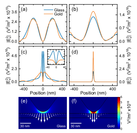
Figure 2 (a,b) describes the far-field (no tip) and (c–f) near-field (with tip) intensity distributions obtained by the frequency-domain modeling, considering the outlined specifics of our experimental setup. The distinction between the field intensity distribution in the presence of glass or gold substrate is obtained, where the blue curves stand for non-gap mode and the orange curves stand for the gap mode configurations in Fig. 2(a–d). The left (a, c) and right (b,d) panels stand for the electric field polarization parallel (X, in-plane) and perpendicular (Z, out-of-plane) to the substrate plane, respectively. In Fig. 2(e,f) the field vectors at the sample’s plane are displayed as white arrows.
Finally, we also performed two-dimensional simulations to understand super-resolution results obtained on the structured gap-mode configuration, where the computational costs get too high due to the loss of the square-lattice plasmonic symmetry. Further details on Section IV.
III Experimental Results and Discussions
III.1 Tip Scanning the Diffraction Limited Confocal Illumination Area
In conventional TERS setups the AFM gold tip is aligned and fixed with respect to the laser focus, and the sample is moved along the XY plane by a piezo stage. In order to study the TERS spatial distribution around the laser focus, we scanned the focal region in the XY plane by moving the tip with respect to the fixed laser spot (and sample), measuring the Raman signal intensity of graphene’s 2D band. This procedure was made for the graphene on glass (non-gap mode) and for the graphene on top of the thin gold film (gap mode). By plotting the 2D band intensity as a function of tip position, we identify the spatial distribution of the convolution between near-field tip response and laser spot, as shown in Fig. 3(a,b). The maximum 2D band TERS intensity is obtained in the central () position in both configurations. The full-width at half maximum (FWHM) is smaller in the gap mode configuration: for the glass and for gold, a reduction for the gap mode configuration. Similar (although less intense) results are observed for the G band TERS.
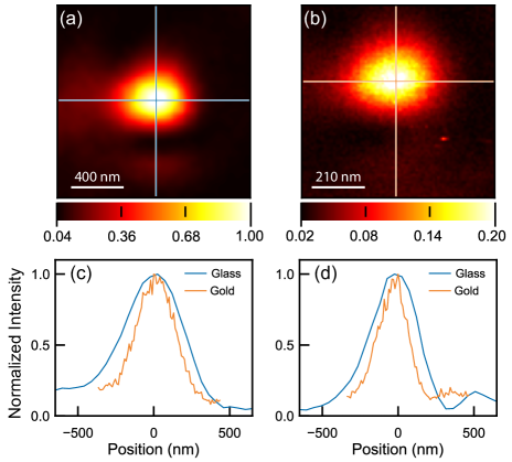
The sharper TERS distribution for gap mode can be understood based on the field distributions shown in Fig. 2. For the far-field (Fig. 2(a,b)) there is a difference in the spread of the in-plane X-polarized field, which is slightly more compressed towards the center, accompanied by a small increase in the very central intensity of the out-of-plane Z-polarized field. For the near-field configuration (Fig. 2(c,d)) the difference also depends on the direction of the electric field. For Z-polarized near-field (d), the field distribution in gap mode is more intense and narrower than for the non-gap mode. For the X-polarized near-field (c), however, it is the opposite when looking closer to the central area under the tip, and the trend in the most intense signal exhibits inversions on each configuration (non-gap mode vs. gap mode, blue and red curves, respectively) as the displacement from the central position increases. Overall, there is a sharper field distribution for the gap mode. The differences in TERS localization are even stronger considering that TERS intensity is proportional to electric field powers up to Yang et al. (2009b). It is important to note, however, that, for this analysis, care has to be taken in proper alignment, since a change (maybe due to experimental drift) in the focus condition between these two experiments can also cause changes in the FWHM.
III.2 Near- and Far-Field Comparison for Different Symmetry Modes and Different Substrates
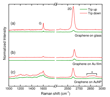
We now analyze how different substrates influence the total spectral enhancement when the tip is placed in the optimal location for TERS signal, i.e. at position in Fig. 3(c,d). The spectral enhancement factor is defined here as , where is the integrated intensity (area) of a Raman peak in the presence of the tip (NF standing for near-field) and the equivalent value in the same region with the tip retracted far away from the sample (FF standing for far-field). Figure 4 shows the graphene Raman spectra with and without the tip on the three different substrates.
The enhancement factors were measured for the G () and 2D () bands on glass, Au film and AuNP substrates, resulting on the values summarized in Table 1.
| Glass | Au film | AuNP | |
|---|---|---|---|
| G | |||
| 2D |
The average results and the uncertainties were obtained analyzing seven tip up and seven tip down spectra like the ones shown in Fig. 4, obtained during a scanning procedure of homogeneous regions (accumulation time of 2 seconds per point for graphene on glass, 5 seconds for graphene on Au film and 10 seconds for graphene on AuNP, excitation power of at the sample for all cases). The estimated uncertainty is larger for the G band on the AuNPs substrate because of the presence of the oleylamine peaks in the second case (see Fig. 4(c), near 1600 cm-1). Interestingly, the enhancement factors change depending on the substrate and the Raman band. Counter-intuitively, the overall enhancement is larger for regular TERS (on glass) as compared to the gap mode configurations, consistent with what has been shown in Fig. 3(a, b).
This counterintuitive result can be understood based on the group theory analysis, combined with the electric field distributions shown in Fig. 2. The presence of the conductive substrate strongly enhances the Z-polarized field, but not the XY-polarized fields. Since graphene responds to electric fields along the plane, the gap mode is actually not effective in enhancing the Raman response of this two-dimensional system. It is important to note that this result implies that the out-of-plane response of totally symmetric (2D) mode, although not symmetry forbidden, is truly negligible, i.e. the Raman tensor parameter (see Eq. 2). As it can be seen in Table 1, while on glass the enhancement factor of the 2D band intensity is 16, on gold it is roughly three times smaller.
Besides, when comparing the results obtained for the G () and 2D () modes, the result on glass is consistent with reports on the literature, where the 2D band enhances more than the G band due to near-field coherence effects that privilege totally symmetric modes Beams et al. (2014); Cançado et al. (2014). Interestingly, this difference washes out in the gap mode configuration, and again, this can be understood as due to the stronger confinement of the field very near the tip location. The inset to Fig. 2(c) shows that, in the gap mode, the in-plane field is strongly reduced close to the tip location, within the phonon coherence length (), where the near-field interference effects take place Beams et al. (2014). This also confirms that the higher enhancement for the 2D band on glass is due to the non-local PS and SP scattering Jorio et al. (2017); Cançado et al. (2014), rather than due to the out-of-plane component of the Raman tensor, otherwise the 2D band should enhance more (not less) in gap mode (see Table 1).
III.3 TERS Line Profile in Structured gap mode
To test field localization and the possible achievement of ultra-high resolution, we measured graphene on top of the AuNP substrate, as described in Section II.2, while scanning the substrate. Since graphene is homogeneously present in this sample, the only variation throughout the scan is the configuration of AuNP underneath the tip’s apex. Figure 5(a) shows the intensity trends of the 2D phonon mode (blue filled bullets) and also the intensity of a nearby Raman band (orange open bullets, cm-1, see * in Fig. 4(c)), attributed to oleylamine, during the line scan. Since the AuNPs are coated by a layer of oleylamine required for the self-assembly into an AuNP monolayer, its Raman band can also be observed.
Considering that the tip used for the experiment shown in Fig. 5 has a diameter, the total scan of is a relatively small scanning region. Still, clear oscillations in the 2D and oleylamine Raman intensities are observed. In terms of lateral resolution, a Fast Fourier Transform analysis of the 2D band intensity map from which the line profile in Fig. 5(a) was taken, results in a spatial resolution of , close to the Nyquist limit of expected for the per pixel sampling rate utilized. This can be considered super-resolution given the apex diameter for the tip utilized in this experiment.
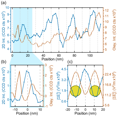
Interestingly, we observe that whenever the intensity of the 2D band increases, the intensity of the oleylamine band decreases. The alternating peak intensity locations when comparing the 2D band and oleylamine bands can be explained considering the intensity profile trends of the in-plane (X) and out-of-plane (Z) components of the electric field as the sample is scanned, as shown in the simulation results in Fig. 5(c) (more detail in Section IV). Note the similarity between the simulation (Fig. 5(c)) and the detailed experimental section in Fig. 5(b). The 2D band is maximum when the in-plane X field is maximum, which happens between particles, while the oleylamine peaks are maximum when the out-of-plane Z field is maximum, which happens on top of a particle.
IV Further Simulations and Discussions on super-resolution
Section III.3 showcases how increased resolution can be obtained from a structured gap mode substrate. In this section, frequency domain simulations using an adapted version of the setup described in Section II.4, limited to two dimensions are used in order to properly characterize the field distribution when “super-resolution” situation is achieved. In the simulation environment, the substrate is modeled by 50 gold circles with a diameter of and a gap between each other.
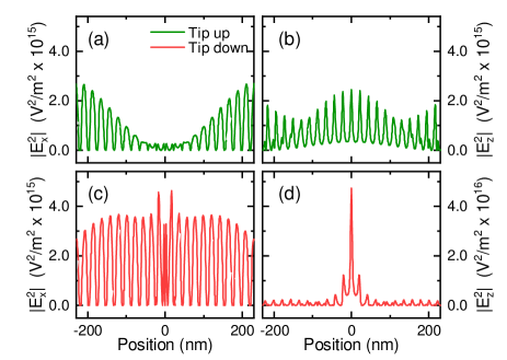
Figure 6 shows a simulated tip up and down experiment. For this structured substrate, the profiles observed in Fig. 2(a-d) are now superposed by modulations induced by the AuNP. When the tip is landed (red traces), there is an increase in field intensity. However, the enhancement is localized near the tip for the out-of-plane Z-field component (Fig. 6(d)), but completely delocalized for the in-plane X-field component (Fig. 6(c)). Therefore, for the experiment shown in Fig. 5(a,b), while the oleylamine spectra comes majorly from molecules localized under the tip, the picture is completely different for the graphene 2D band.
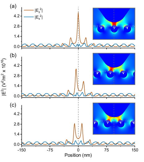
For further details, Fig. 7 shows the changes in the X- and Z-field intensities for different relative position of the tip with respect to the AuNPs, i.e. right on top of a particle (a), exactly in between two particles (c), and between these two cases (b). In all cases, the graphene TERS signal (given by the X-polarized field) should come from the entire focal region, while some degree of localization is only obtained for TERS related to the Z-polarized field component.
V Conclusions
By exploring experimentally and theoretically the TERS electric field distribution in graphene on different substrates, we consistently found that in gap mode configuration a strong Z-polarized field is excited, but it does not generate extra enhancement for 2D systems such as graphene, which responds to electric fields polarized along the substrate plane. Our analysis solidifies the conclusion that the totally symmetric modes in graphene have a negligible Raman response for fields polarized perpendicular to the graphene plane, even if not symmetry forbidden. Furthermore, we show that near-field interference effects are suppressed for the in-plane fields in gap mode.
Additionally, it was shown, both by simulations and experiments, that the composition of the substrate has an effect on field confinement and, consequently, on resolution. Nevertheless, the resolution can be further improved, beyond the tip’s apex diameter, by means of a careful choice of the tip-sample-substrate interaction. For instance, a conductive substrate with features smaller than the tip’s apex, such as gold nanoparticles, can be employed to improve the lateral resolution, but this is effective only for the out-of-plane polarized field. However, the substrate actually delocalizes the in-plane electric field. This effect must be carefully considered when analysing sub-nanometer TERS measurements, as the tip will still interact with all sub-nanometer features in its vicinity. Although our results were developed for nanometer-size structures, similar effects should be observed in pico-cavity measurements Lee et al. (2019); Baumberg et al. (2019).
VI Acknowledgements
This work was supported by the Fundação Coordenação de Aperfeiçoamento de Pessoal de Nível (CAPES) and the Deutsche Akademische Austauschdienst (DAAD) within the PROBRAL program under grant number 57446501. A.J. acknowledges financial support from the Humboldt Foundation and CNPq (552124/2011-7, 307481/2013-1, 304869/2014-7, 460045/2014-8, 305384/2015-5, 309861/2015-2. H.M. and C.R. acknowledges financial support from Finep, CNPq and Fapemig. P.K. and S.R. acknowledge support by the European Research Council ERC under grant DarkSERS (772108) and the Focus Area NanoScale of Freie Universität.
References
- Wessel (1985) J. Wessel, JOSA B 2, 1538 (1985).
- Stöckle et al. (2000) R. M. Stöckle, Y. D. Suh, V. Deckert, and R. Zenobi, Chemical Physics Letters 318, 131 (2000).
- Hartschuh et al. (2003a) A. Hartschuh, E. J. Sánchez, X. S. Xie, and L. Novotny, Physical Review Letters 90, 095503 (2003a).
- Hartschuh et al. (2003b) A. Hartschuh, N. Anderson, and L. Novotny, Journal of Microscopy 210, 234 (2003b).
- Hagen et al. (2005) A. Hagen, M. Steiner, M. B. Raschke, C. Lienau, T. Hertel, H. Qian, A. J. Meixner, and A. Hartschuh, Physical Review Letters 95, 197401 (2005).
- Maciel et al. (2008) I. O. Maciel, N. Anderson, M. A. Pimenta, A. Hartschuh, H. Qian, M. Terrones, H. Terrones, J. Campos-Delgado, A. M. Rao, L. Novotny, and A. Jorio, Nature Materials 7, 878 (2008).
- Bailo and Deckert (2008) E. Bailo and V. Deckert, Chemical Society Reviews 37, 921 (2008).
- Cançado et al. (2009) L. G. Cançado, A. Hartschuh, and L. Novotny, Journal of Raman Spectroscopy 40, 1420 (2009).
- Yeo et al. (2009) B.-S. Yeo, J. Stadler, T. Schmid, R. Zenobi, and W. Zhang, Chemical Physics Letters 472, 1 (2009).
- Yano et al. (2009) T. A. Yano, P. Verma, Y. Saito, T. Ichimura, and S. Kawata, Nature Photonics 3, 473 (2009).
- Van Schrojenstein Lantman et al. (2012) E. M. Van Schrojenstein Lantman, T. Deckert-Gaudig, A. J. Mank, V. Deckert, and B. M. Weckhuysen, Nature Nanotechnology 7, 583 (2012).
- Kumar et al. (2015) N. Kumar, B. Stephanidis, R. Zenobi, A. J. Wain, and D. Roy, Nanoscale 7, 7133 (2015).
- Park et al. (2016) K.-D. Park, O. Khatib, V. Kravtsov, G. Clark, X. Xu, and M. B. Raschke, Nano Letters 16, 2621 (2016).
- Wang et al. (2017) X. Wang, S.-C. Huang, T.-X. Huang, H.-S. Su, J.-H. Zhong, Z.-C. Zeng, M.-H. Li, and B. Ren, Chem. Soc. Rev. 46, 4020 (2017).
- Beams (2018) R. Beams, Journal of Raman Spectroscopy 49, 157 (2018).
- Yang et al. (2009a) Z. Yang, J. Aizpurua, and H. Xu, Journal of Raman Spectroscopy 40, 1343 (2009a).
- Deckert (2009) V. Deckert, Journal of Raman Spectroscopy 40, 1336 (2009).
- Shi et al. (2017) X. Shi, N. Coca-López, J. Janik, and A. Hartschuh, Chemical Reviews 117, 4945 (2017).
- Chen et al. (2014) C. Chen, N. Hayazawa, and S. Kawata, Nature communications 5, 3312 (2014).
- Zhang et al. (2013a) R. Zhang, Y. Zhang, Z. Dong, S. Jiang, C. Zhang, L. Chen, L. Zhang, Y. Liao, J. Aizpurua, and Y. e. Luo, Nature 498, 82 (2013a).
- Lee et al. (2019) J. Lee, K. T. Crampton, N. Tallarida, and V. A. Apkarian, Nature 568, 78 (2019).
- Baumberg et al. (2019) J. J. Baumberg, J. Aizpurua, M. H. Mikkelsen, and D. R. Smith, Nature Materials 18, 668 (2019).
- Zhang et al. (2007) W. Zhang, B. S. Yeo, T. Schmid, and R. Zenobi, The Journal of Physical Chemistry C 111, 1733 (2007).
- Stadler et al. (2013) J. Stadler, B. Oswald, T. Schmid, and R. Zenobi, Journal of Raman Spectroscopy 44, 227 (2013).
- Zhang et al. (2013b) R. Zhang, Y. Zhang, Z. C. Dong, S. Jiang, C. Zhang, L. G. Chen, L. Zhang, Y. Liao, J. Aizpurua, Y. Luo, J. L. Yang, and J. G. Hou, Nature 498, 82 (2013b).
- Vasconcelos et al. (2015) T. L. Vasconcelos, B. S. Archanjo, B. Fragneaud, B. S. Oliveira, J. Riikonen, C. Li, D. S. Ribeiro, C. Rabelo, W. N. Rodrigues, A. Jorio, C. A. Achete, and L. G. Cançado, ACS Nano 9, 6297 (2015).
- Vasconcelos et al. (2018) T. L. Vasconcelos, B. S. Archanjo, B. S. Oliveira, R. Valaski, R. C. Cordeiro, H. G. Medeiros, C. Rabelo, A. Ribeiro, P. Ercius, C. A. Achete, A. Jorio, and L. G. Cançado, Advanced Optical Materials 6, 1800528 (2018).
- Becker et al. (2016) S. F. Becker, M. Esmann, K. W. Yoo, P. Gross, R. Vogelgesang, N. K. Park, and C. Lienau, ACS Photonics 3, 223 (2016).
- Jorio et al. (2011) A. Jorio, R. Saito, G. Dresselhaus, and M. S. Dresselhaus, Raman Spectroscopy in Graphene Related Systems (Wiley-VCH Verlag GmbH & Co. KGaA, Weinheim, Germany, 2011).
- Jorio et al. (2019) A. Jorio, L. G. Cançado, S. Heeg, L. Novotny, and A. Hartschuh, in Handbook of Carbon Nanomaterials, edited by R. B. Weisman and J. Kono (World Scientific, 2019) 1st ed., Chap. 5, pp. 175–221.
- Schulz et al. (2017) F. Schulz, S. Tober, and H. Lange, Langmuir 33, 14437 (2017).
- Mueller et al. (2018) N. S. Mueller, B. G. Vieira, F. Schulz, P. Kusch, V. Oddone, E. B. Barros, H. Lange, and S. Reich, ACS Photonics 5, 3962 (2018).
- Budde et al. (2016) H. Budde, N. Coca-López, X. Shi, R. Ciesielski, A. Lombardo, D. Yoon, A. C. Ferrari, and A. Hartschuh, ACS Nano 10, 1756 (2016).
- Jorio et al. (2017) A. Jorio, N. S. Mueller, and S. Reich, Physical Review B 95, 155409 (2017).
- Novotny and Hecht (2012) L. Novotny and B. Hecht, Principles of Nano-Optics (Cambridge University Press, Cambridge, 2012).
- Johnson and Christy (1972) P. B. Johnson and R. W. Christy, Physical Review B 6, 4370 (1972), arXiv:arXiv:1011.1669v3 .
- Yang et al. (2009b) Z. Yang, J. Aizpurua, and H. Xu, Journal of Raman Spectroscopy 40, 1343 (2009b).
- Beams et al. (2014) R. Beams, L. G. Cançado, S.-H. Oh, A. Jorio, and L. Novotny, Physical Review Letters 113, 186101 (2014).
- Cançado et al. (2014) L. G. Cançado, R. Beams, A. Jorio, and L. Novotny, Physical Review X 4, 031054 (2014).