Control-Bounded Analog-to-Digital Conversion:
Transfer Function Analysis, Proof of Concept,
and Digital Filter Implementation
Abstract
Control-bounded analog-to-digital conversion has many commonalities with delta-sigma conversion, but it can profitably use more general analog filters. The paper describes the operating principle, gives a transfer function analysis, presents a proof-of-concept implementation, and describes the digital filtering in detail.
Index Terms:
analog-to-digital conversion, chain of integrators, continuous time delta-sigma modulator, factor graphs, Kalman smoothing, Wiener filter.I Introduction
Based on control-aided analog-to-digital conversion as in [1], control-bounded analog-to-digital conversion was proposed in [2]. The general structure of such an analog-to-digital converter (ADC) is shown in Figure 1: the continuous-time analog input signal (or as in (1)) is fed into an analog linear system/filter, which is subject to digital control. The digital control ensures that all analog quantities, including, in particular, the signals , …, , remain within their proper physical limits. Using the digital control signals , …, , the digital estimation unit tracks the state of the analog system and produces (arbitrarily spaced samples of) an estimate of . The analog signals , …, , which are not available to the digital estimator, play a key role in the estimation as will be detailed in Section II.
In the important special case shown in Figure 2, the -valued control signals , …, are obtained by sampling and thresholding the analog signals , which include the control-bounded signals , …, , .
As may be conjectured from Figure 2, control-bounded converters may be viewed as generalizations of delta-sigma () converters [3]. Indeed, for , a control-bounded converter as in Figure 2 has no advantage over a standard converter. For , however, control-bounded converters can use analog systems/filters that cannot be handled by conventional techniques.
The descriptions in [1, 2] are terse and may not be easily accessible to analog designers. Moreover, the transfer function analysis in [2] covers only the case , the performance analysis in [2] is rudimentary, and no measurements of a real circuit are reported.
In this paper, we describe the operating principle and the digital estimation filter in more detail, we give a full transfer function analysis, and we report measurements of a breadboard circuit prototype. In particular, this paper provides sufficient information for analog designers to experiment with control-bounded ADCs.
Much space will be given to the analysis of a single example: digital control, noise and mismatch properties, simulations, and measurements of the hardware prototype. This example—a chain of integrators as in [2]—closely resembles a multi-stage noise shaping (MASH) ADC [7, 8], but with an analog part that precludes a conventional digital cancellation scheme. (Other analog circuit topologies with attractive properties will be described elsewhere.)
The paper is structured as follows. The operating principle and the basic transfer function analysis of control-bounded converters are given in Section II. A conversion noise analysis is given in Section III. The circuit example is presented and analyzed in Section IV. Some enhancements (including, in particular, a tailored dithering method) are discussed in Section V. The sensitivity to thermal noise and component mismatch is considered in Section VI. The digital estimation filter is described in Section VII. The actual derivation of this filter is outlined in the Appendix.
II Operating Principle
II-A Analog Part and Digital Control
Consider the system of Figure 1. The continuous-time input signal is assumed to be bounded, i.e., for all times . More generally, the input signal may be a vector
| (1) |
with bounded components for all and . The analog linear system produces a continuous-time vector signal
| (2) |
and the digital control in Figure 1 ensures that
| (3) |
We also assume that the digital control is additive, i.e.,
| (4) |
where (given by (6) below) is the fictional signal that would result without the digital control and where is fully determined by the control signals , …, .
At this point, we have already finished the discussion of the digital control in this section: its role and its effect are fully described by (3) and (4).
Clearly, neither nor are bounded by . In fact, the first key idea of control-bounded conversion is to use as a proxy for , and this approximation will be good only if the magnitude of is much larger than the magnitude of (as will be made precise below). Note that may be very complicated, but it is, in principle, known to the digital estimator since is fully determined by , …, .
We now assume that the uncontrolled analog filter is time-invariant and stable111The extension of the following transfer function analysis to unstable analog systems is possible, but beyond the scope of this paper. with impulse response matrix
| (5) |
where is the impulse response from to . We then have
| (6) | |||||
| (7) |
We will also need the (elementwise) Fourier transform of (5), which will be denoted by and will be called analog transfer function (ATF) matrix.
II-B Digital Estimation and Transfer Functions
Using the impulse response matrix defined in (13) below, we define the continuous-time estimate
| (8) |
which can be written as
| (9) | |||||
| (10) | |||||
| (11) |
Note that the step from (9) to (10) uses the mentioned approximation , or, equivalently, the approximation
| (12) |
as illustrated in Figure 1.
The impulse response matrix is determined by its (elementwise) Fourier transform
| (13) |
where denotes Hermitian transposition, is the -by- identity matrix, and is a design parameter. Each element of is stable, and arbitrarily spaced samples of (8) can be computed from the control signals , …, as will be described in Section VII.
Equations (9) and (11) can then be interpreted as follows. Eq. (11) is the signal path: the signal is filtered with the signal transfer function (STF) matrix
| (14) |
The second term in (9) is the conversion error
| (15) | |||||
| (16) |
with bounded as in (3). Because of (16), will be called noise transfer function (NTF) matrix.
In the important special case where is scalar (i.e., ), the ATF matrix is a column vector and the NTF matrix (13) is a row vector. Using the matrix inversion lemma, the latter can be written as
| (17) |
and the STF matrix (14) reduces to the scalar STF
| (18) |
Note that (18) does not entail a phase shift and is free of aliasing (hence the title of [2]): the sampling in Figure 1 (which is used for the digital control) affects the error signal (16), but not (11).
II-C Bandwidth and the Parameter
For the following discussion of the parameter in (13) and (14), we restrict ourselves to the scalar-input case, where the STF and the NTF are given by (18) and (17), respectively. In this case, it is easily seen from (18) that determines the bandwidth of the estimate (8). For example, assuming that decreases with , the bandwidth is roughly given by with determined by
| (19) |
II-D Remarks
We conclude this section with a number of remarks. First, we note that he conversion error (15) is not due to the quantizers in Figures 1 and 2, but due to approximating the control-bounded signals by zero as in (12). In particular, the quantized signals are not used as noisy observations of (some filtered version of) , but only to determine the digital control. In consequence, the quantizer circuits need not be implemented with high precision.
Second, the STF (14) and (18) is an exact continuous-time result. By contrast, continuous-time modulators are typically first designed in discrete time and then converted into continuous time using concepts such as direct filter synthesis [12].
Finally, the digital estimation and the transfer function analysis of Section II-B work for arbitrary stable analog transfer functions . In fact, stability of the uncontrolled analog system has here been assumed only for the sake of the analysis: the actual digital filter in Section VII is indifferent to this assumption. Moreover, the details of the digital control (clock frequency, thresholds, etc.) do not enter the transfer function analysis. This generality offers design opportunities for the analog system/filter beyond the limitations of conventional modulators.
III Conversion Noise Analysis
In this section, we (again) restrict ourselves to the case where is scalar (i.e., ) and will be denoted by . While the analysis in Section II was mathematically exact, we are now prepared to use approximations similar to those routinely made in the analysis of ADCs.
III-A SNR and Statistical Noise Model
Disregarding circuit imperfections (which will be addressed in Section VI), the quantization performance can be expressed as the signal-to-noise ratio (SNR)
| SNR | (21) |
where and are the power of and the power of the conversion error (16), respectively, both within some frequency band of interest.
The numerator in (21) depends, of course, on the input signal. A trivial upper bound is , and for a full-scale sinusoid, we have
| (22) |
As for the in-band power of the conversion error (16), we begin by writing
| (23) |
where is modeled as a stationary stochastic process with power spectral density matrix
| (24) |
(These statistical assumptions cannot be literally true, but they are a useful model.) Restricting (23) to the frequency band of interest, we have
| (25) |
III-B White-Noise Analysis
If in (25) is approximated by
| (26) |
we further obtain
| (27) | |||||
| (28) | |||||
| (29) |
where the last step is justified by for , cf. (18) and Section II-C.
IV Example: Chain of Integrators
In the following sections, we focus on the specific example shown in Figure 3. (We will return to the general case in Section VII.) This example was first presented in [2], but it is here analyzed much further. Other analog circuit topologies with attractive properties will be presented elsewhere.
IV-A Analog Part and Digital Control
The analog part including the digital control is shown in Figure 3. The input signal is a scalar. The state variables , …, obey the differential equation
| (30) |
with , , and with . The switches in Figure 3 represent sample-and-hold circuits that are controlled by a digital clock with period . The threshold elements in Figure 3 produce the control signals depending on the sign of at sampling time immediately preceding .
We will assume , and the system parameters will be chosen such that
| (31) |
holds for .
The control-bounded signals are selected from the state variables (cf. Figure 2), as will be discussed in Section IV-D below.
IV-B It’s not a MASH Converter
The system of Figure 3 has some similarity with a continuous-time MASH modulator [11]. However, Figure 3 cannot be handled by conventional cancellation schemes. To see this, consider Figure 4, which shows how the first stage in Figure 3 would conventionally be modeled (perhaps with ), where is the local quantization error [3]. Since enters the system in exactly the same way as (except for a scale factor), these two signals cannot be separated by any subsequent processing.
By contrast, the digital estimation of Section II-B cancels the effect of on in all stages () and is indifferent to the existence of a conventional cancellation scheme.
IV-C Conditions Imposed by the Digital Control
IV-D Transfer Functions
As mentioned, the control-bounded signals are selected from the state variables . An obvious choice is and , …, . In this case, the ATF of the uncontrolled analog system (as defined in Section II) is given by
| (37) |
Another reasonable choice is and as in [2]. In this case, the ATF is simply
| (38) |
We now specialize to the case where and , which makes the analysis more transparent. For as in (38), we then have
| (39) |
For , we obtain
| (40) | |||||
| (41) |
Note that, for , as in (39) is the dominant term in (40). In consequence, as in (39) yields almost the same performance as (40).
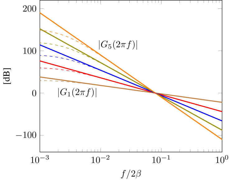
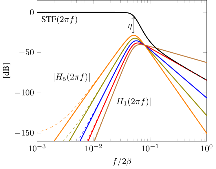
For illustration, the amplitude responses , …, are plotted in Figure 10 for , , and . Figure 10 shows the resulting STF (18) and the components , …, of the NTF (17) for (i.e., with as in (41)) and .
From now on, we will normally assume (i.e., undamped integrators).
IV-E Bandwidth
IV-F Simulation Results
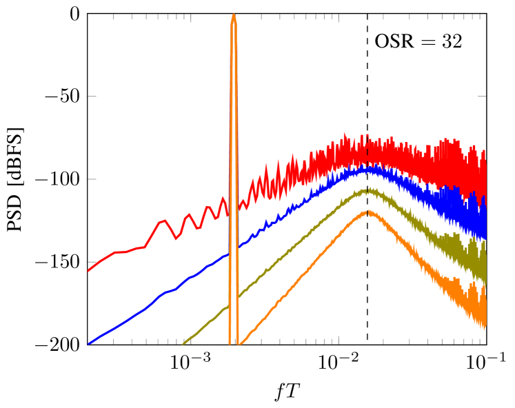
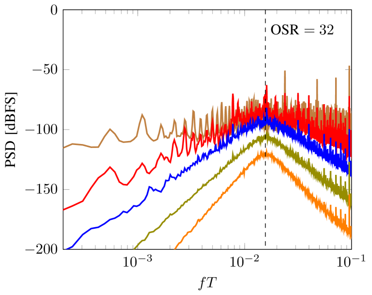
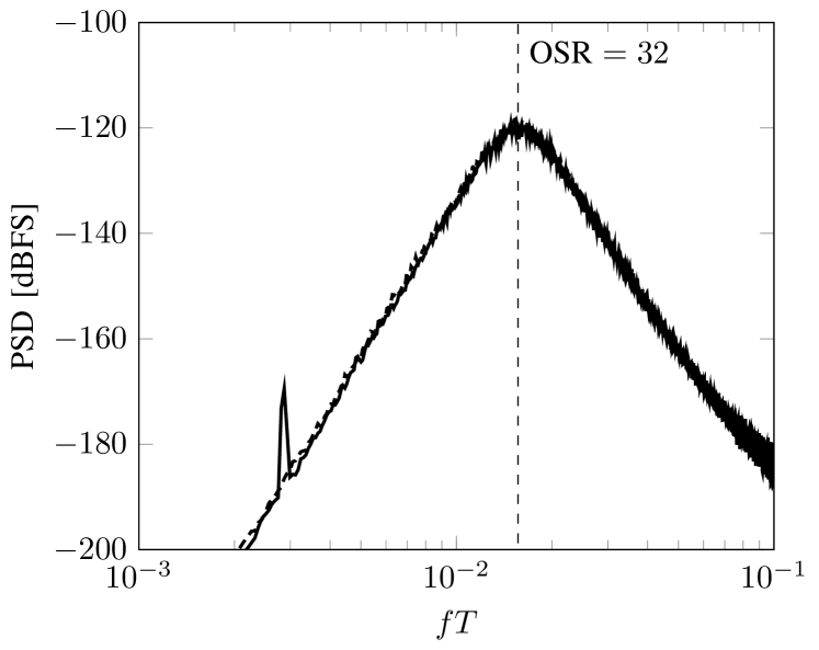
Figures 10 and 10 show the power spectral density (PSD) of the digital estimate for the numerical example in Figures 10 and 10 with and with further details as given below. In Figure 10, the input signal is a full-scale sinusoid; in Figure 10, the input signal is . Except for the peak in Figure 10, both Figure 10 and Figure 10 thus show the PSD of the conversion error (15).
As for the details in these simulations, we have , , , and , resulting in . The frequency of the sinusoidal input signal is Hz.
The conspicuous fluctuations in the power spectral density for can be suppressed by dithering as described in Section V-A.
A key point of Figures 10 and 10 is that the PSD of the conversion error (after suitable smoothing by dithering) appears to be well described by the white-noise analysis of Section III-B, which will be further developed in Section IV-G.
The resulting SNR (21), as a function of the amplitude of the sinusoidal input signal , is shown in Figure 10. Also shown in Figure 10 is an approximate analytical expression for the SNR that will be discussed in Section IV-G. Note that the SNR collapses when the input signal amplitude exceeds the bound .
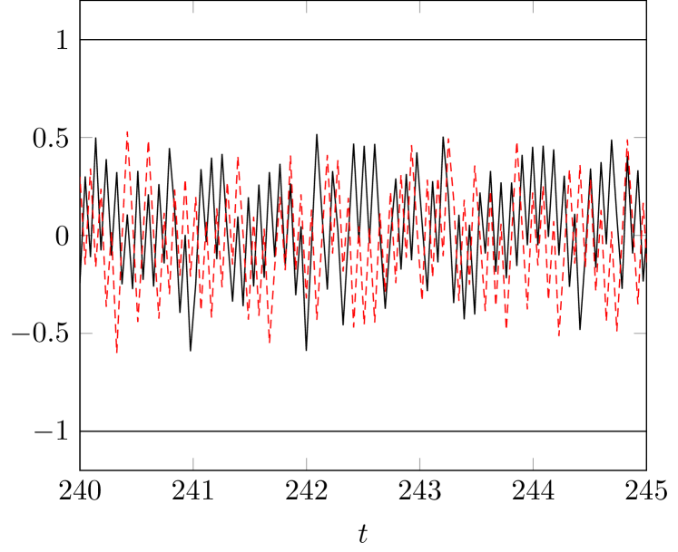
Figure 10 shows the signal for two different input signals : one of the input signals is a sinusoid with frequency Hz and amplitude and the other is . The point is that the two signals look very much alike: like two different realizations of the same stochastic process. Note also that the digital control, which guarantees , appears to be quite conservative.
IV-G White-Noise Analysis
In the following, we use as in (39) (with ), which also serves as an approximation of (40) provided that . The integral in (29) is then easily determined analytically:
| (47) | |||||
| (48) |
Using (44) and (43), we further obtain
| (49) | |||||
| (50) |
We next approximate the in-band noise power by
| (51) |
with an unknown scale factor . The factor in (51) accounts for the bounded amplitude of , cf. (22). The factor in (51) accounts for the fact that, for large , the signal originates primarily from the control signals , cf. Figure 10. Specifically, since is fixed (for all ), the power spectral density222Note that we here view as stationary stochastic processes. This cannot be literally true, but it is a useful model. Such assumptions/models are standard in the literature. of scales with . Since is essentially created by by linear filtering, the power spectral density of scales with as well.
IV-H Proof of Concept with Hardware Prototype
Figures 12 and 12 show some results with a hardware prototype as in Figure 14 that was built with discrete components. The only purpose of this prototype was to verify the basic functionality of such a converter; it was not designed to excel in terms of speed, accuracy, or power consumption.
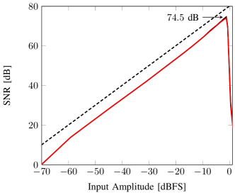
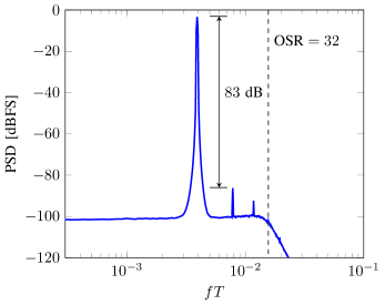
Specifically, Figure 12 shows the measured SNR and SNDR (signal-to-noise-and-distortion ratio) for a sinusoidal input of frequency Hz, and Figure 12 shows the PSD for the measurement corresponding to the largest SNDR in Figure 12. We thus have a spurious-free dynamic range (SFDR) of approximately 83 dB as well as a SNDR of dB.
The prototype implements the system of Figure 3 with nominally identical stages and with a little additional feedback to the first stage as in Figure 14 (cf. Section V-A). The integrators are realized with an operational amplifier (AD8615) as shown in Figure 13. The control period is chosen as s. The nominal value of the capacitor is 10 nF and the nominal value of both resistors ( and ) is 16 k, resulting in and . For the first stage, the feedback contributions are k. The operating voltage is 5V, but all signals are confined to the range 0…2.5 V; “zero” in Figure 3 translates to V. The resistors and capacitors are standard surface-mount devices with 1% tolerance; they were not preselected and their actual values were not measured.
The control signal (i.e., the voltage in Figure 13) is generated from using a separate threshold circuit (TLV3201) and a separate analog switch (TS5A9411). The whole circuitry is realized on a printed circuit board, which is piggybacked on an Arduino board.
For the empirical results shown in Figures 12 and 12, the digital filter (as described in Section VII) works with nominal values of and ; neither the hardware prototype nor the digital filter use any calibration or adjustment for actual (rather than nominal) values. (See also Section V-B).
The parameter of the digital filter is set according to (45) with .
V Enhancements
V-A Limit Cycles and Dithering by Extra Digital Feedback
Analog systems as in Figures 2 and 3 may have limit cycles [8], which lead to distinct peaks in the power spectrum. For example, Figure 15 shows the PSD of as in Figures 10 and 10, but with constant input signal (and only for ): the conspicuous peak at is due to a limit cycle.
A standard strategy against limit cycles is to use some sort of dithering [13, 14, 15, 16]. Control-bounded converters as in this paper offer convenient ways to do this without actually adding noise to the estimate .
A first method is to add “random” dither to the thresholds for the control signals in Figures 2 or 3. This method does not affect the analysis of Section II and is irrelevant for the digital estimation filter.
A second method, shown in Figure 14, is to feed small contributions of all the controls back to the first stage. This method relies on the effective randomness of the control signals for large and obviates the need of an extra source of randomness. Extensive simulations (as exemplified in Figure 15) have shown this method to be highly effective. Note that the augmented system as in Figure 14 still fits into the general scheme of Figure 1. In particular, the extra feedback signals are known to the digital estimation filter, which can remove their effect on the analog signals.
When implementing this method, it should be noted that the extra feedback reduces the allowed amplification for guaranteed stability of the first stage. However, this reduction is minor as the extra feedback can be quite small and yet effective.
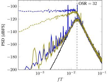
V-B Helps Against Mismatch, Too
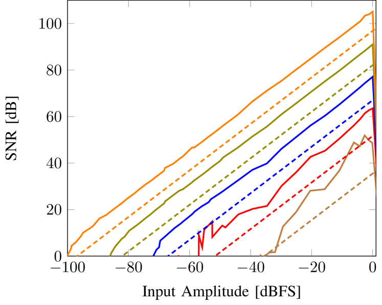
Extra digital feedback as in Figure 14 turns out also to significantly mitigate the effects of component mismatch. For example, the colored solid lines in Figure 16 show the dramatic effect of (simulated) component mismatch on the PSD of for . Adding extra digital feedback as in Figure 14 raises the floor of the PSD of but removes the detrimental peaks, resulting in a huge net reduction of the conversion noise. Extensive simulations have shown that this works quite generally. In particular, the good experimental results with the hardware prototype shown in Figures 12 and 12 cannot nearly be achieved without this trick.
V-C Improving the Scaling in (52)
Except for the factor , the SNR (52) scales with like in a typical converter, cf. [8], Eq. (4), (7), and (8). Recall also (from Sections IV-C and IV-E) that for guaranteed stability. However, can be increased beyond in two different ways as follows.
V-C1 Venturing Beyond Stability
As illustrated in Figure 10, the conditions for control as in Section IV-C may be rather pessimistic. Increasing beyond 1/2 may thus be ventured for . (It should be remembered that conventional high-order converters come without stability guarantee.) However, we have not systematically explored this option.
V-C2 Multi-level Quantizers
Replacing the single-bit quantizers in Figure 3 by multi-level quantizers makes the control more effective and thereby allows for additional amplification at each stage. Specifically, using -bit quantizers allows to increase up to
| (53) |
For large , we thus obtain .
VI Thermal Noise and Component Mismatch
The analysis of Sections III and IV-G can be extended to include also thermal noise and component mismatch, along lines familiar from the analysis of converters. As in Section III, we restrict ourselves to the case where is scalar (i.e., ).
VI-A Thermal Noise
Let be a single thermal noise signal entering at some point in the analog system and let be the vector of impulse responses from this noise source to . Thus (4) is modified into
| (54) |
In consequence, (9) is modified into
| (55) | |||||
| (56) |
where the term
| (57) |
is the additional error due to .
Assume now that, within the frequency band of interest, is white with power spectral density
| (58) |
The contribution of (57) to the noise power (25) is then easily determined to be
| (59) | |||||
| (60) |
where is the (elementwise) Fourier transform of .
Finally, the total contribution of multiple such thermal noise sources to the noise power (25) is simply .
VI-B Mismatch
Let , , and be the nominal (i.e., assumed) values of the actual quantities , , and , respectively. We still have
| (61) |
but we now have
| (62) | |||||
| (63) | |||||
| (64) |
The total conversion error can then be written as
| (66) | |||||
The three terms in (66) are of a very different nature. The last term, , is the nominal conversion error (16), to which the analysis in Section III applies essentially unchanged. In other words, the contribution of this term to the in-band noise power (25) is basically unaffected by the mismatch.
The first term in (66),
| (67) |
accounts for a modification of the STF. In principle, this term can be neutralized by calibrated postfiltering. If this term is considered as noise, its magnitude obviously depends on the signal . If we assume to be white noise (within the band of interest), the contribution of (67) to the in-band noise power can be expressed by an obvious modification of (59).
The second term in (66) is more troublesome:
| (68) | |||||
| (69) |
where and are the nominal and the actual transfer functions, respectively, from to .
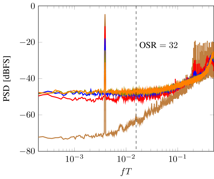
If we boldly assume to be white (within the band of interest), the contribution of (69) to the in-band noise power can also be expressed by an obvious modification of (59). However, the white-noise assumption may be too bold, cf. Figure 17. In any case, the power spectral density of (for a specific input signal ) can be determined by simulations, as demonstrated in Figure 17.
VI-C Application to the Circuit Example
We now briefly discuss thermal noise and mismatch for the circuit example of Section IV (Figs. 3 and 14) with integrators as in Figure 13. For the sake of clarity, we restrict ourselves to the case , i.e., is the only control-bounded signal used by the digital estimation.
The transfer function from any noise source at stage to is
| (70) |
with for thermal noise and with or for mismatch in the resistors in Figure 13, where and denote the nominal values while and denote the actual values. The product of (70) and the NTF (17) is the the transfer function from the error source to the estimate .
In the hardware prototype of Section IV-H, all stages (i.e., all integrators) were dimensioned equally. Therefore, the prototype will be sensitive primarily to errors introduced in the first stage of the chain.
Using the analysis of Section VI-A, at room temperature, the thermal noise caused by the two resistors in Figure 13 should cause a noise floor in at about dB. It is thus obvious from Figure 12 that thermal noise is not the primary limitation of the prototype.
Indeed, the prototype is probably limited primarily by component mismatch. In principle, the analysis of Section VI-B applies, but the PSD of the control signals (as illustrated in Figure 17) defies a simplistic white-noise assumption. In particular, the PSD of the first-stage control signal is very favorably shaped, and this observation seems to be quite stable over different experimental scenarios.
VII Computing
The job of the digital estimation in Figure 1 is to compute samples of the continuous-time estimate defined by (8) and (13). At first sight, this computation looks daunting, involving not only the continuous-time convolution (8), but also the computation of from the control signals .
It turns out, however, that samples of can be computed quite easily and efficiently by the recursions given in Section VII-B below. A brief derivation of these recursions is given in the Appendix; in outline, it involves the following steps. The starting point is that the filter (13) is formally identical with the optimal filter (the Wiener filter) [6][18] for a certain statistical estimation problem. This same statistical estimation problem can also be solved by a variation of Kalman smoothing [6], which leads to recursions based on a state space model of the analog system. The precise form of the required Kalman smoother is not standard, however, and it combines input signal estimation as in [4] with a limit to continuous-time observations.
VII-A State Space Representation of the Analog System
We will need a state space representation of the analog system/filter in Figure 1 of the form
| (71) |
and
| (72) |
with state vector , with , and with real matrices , , , and of suitable dimensions. The matrix will be required to be regular. (As a rule, this regularity condition is satisfied for ordinary analog filters.)
VII-B Filter Algorithm
Assume now that we wish to compute for We will here restrict ourselves to regular sampling333In this section, we use to index time steps, which is unrelated to the dimensionality of as in (1). with such that (the period of the clock in Figures 1 and 3) is an integer multiple of ; in other words, we interpolate regularly between the ticks of the clock in Figure 1. (In most practical applications, will do.) Moreover, we focus on the steady-state case where border effects can be neglected. The algorithm consists of a forward recursion and a backward recursion.
-
Forward recursion: for compute the vectors (of the same dimension as ) by
(84) starting from .
The required matrices and will be given in Section VII-E.
-
Backward recursion: Compute the vectors (of the same dimension as ) by
(85) starting from for some , as well as
(86)
The required matrices and and the matrix will be given in Section VII-E. For the sake of computational efficiency, the same starting point for the backward recursion will typically be used to compute (86) for a range of consecutive indices .
VII-C FIR Filter and Mixed IIR/FIR Filter Version
The computation of (as described above) can also be organized as a finite impulse response (FIR) filter or as a mixed IIR/FIR filter. For the sake of clarity, we consider only the case , i.e., . For the mixed-filter version, we write (86) as
| (87) |
with
| (88) |
and where the latency parameter replaces . For the FIR version, the term in (87) is expanded analogously.
VII-D Fully Parallel IIR Filter Version
Equations (84), (85) and (86) can also be casted as a fully parallel version where
| (89) | |||||
| (90) |
and
| (91) |
Note that (89), (90) and (91) are all scalar expressions. The index in (89)–(91) and the index in (91) refer to the components of the respective vectors. The coefficients and are obtained from the eigenvalue decomposition
| (92) | |||||
| (93) |
where and are the eigenvalues of and respectively. The scalar functions and are the -th elements of the vectorized functions
| (94) | |||||
| (95) |
and and are the -th elements of the matrices
| (96) | |||||
| (97) |
VII-E Offline Computations
We first need the symmetric square matrices and (of the same dimension as ) as follows. The matrix is the limit
| (98) |
of the iteration
| (99) | |||||
equivalently, is the solution of the continuous-time algebraic Riccati equation
| (100) |
The matrix is defined almost identically, but with a sign change in , i.e., is the solution of the continuous-time algebraic Riccati equation
| (101) |
The matrix in (84) is given by
| (103) |
and the matrix in (85) is
| (104) |
Finally, the matrix in (84) is
| (105) |
and the matrix in (85) is
| (106) |
Note that the only free parameter of the digital filter is as in (13).
Care must be taken that the quantities of this section are computed with sufficient numerical precision, and the matrices and should be exactly symmetric.
VIII Conclusion
We have developed the principles, and discussed many details, of control-bounded analog-to-digital conversion. Such converters have many commonalities with converters, but they can employ analog systems/filters for which no traditional cancellation scheme exists. While we gave an example of such an ADC (in Section IV), it should be clear that many other circuit topologies are possible. (Some such topologies with attractive properties will be presented elsewhere.) The present paper provides sufficient information for analog designers to experiment with such ADCs.
[Brief Derivation of the Digital Filter Algorithm]
In this appendix, we give a condensed derivation of the algorithm of Section VII. (A detailed development of all the required background is beyond the scope of this paper.)
We first observe that the filter (13) is formally a multivariate extension of the continuous-time Wiener filter [18] that estimates a multivariate zero-mean white Gaussian noise “signal” from the signal
| (113) |
where is -dimensional zero-mean white Gaussian noise that is independent of . In this statistical model, the average
| (114) |
(for ) is a -dimensional444In this appendix, we use , rather than as in (1), to denote the number of input signals. zero-mean Gaussian random variable with covariance matrix . The covariance matrix of is defined analogously.
By “estimating ”, we really mean to estimate the random variable(s) (114) for any fixed , and then taking the limit [5]. In this setting, the MAP estimate, the MMSE estimate, and the LMMSE estimate agree and equal the mean of the posterior distribution of conditioned on the observation of . The Wiener filter computes this estimate (for ) as
| (115) |
where the Fourier transform of is (13) with
| (116) |
Applying this Wiener filter to the signal as in (8) means that we solve the statistical estimation problem for the observation .
The same statistical estimation problem can also be solved by a variation of Kalman smoothing. In constrast to the Wiener filter, the Kalman approach is based on the state space equations (71) and (72), which leads to recursive estimation algorithms. We will use a discrete-time approximation of the state space model with discrete times555The discrete times in this appendix (with ) are unrelated to the discrete time steps in Section VII. and fixed ; our continuous-time results will then be obtained by taking the limit .
From now on, we will use factor graphs as in [19], which allow to compose recursive estimation algorithms from lookup tables of “local” computations. A factor graph of (the discrete-time approximation of) our statistical model in state space form is shown in Figure 18. Note that Figure 18 represents the uncontrolled analog system with the observations .
Now we plug in the (known and piecewise constant) control signals into the state space model. We thus obtain the factor graph of Figure 19, where all the observed signals are now zero, cf. (12). This second factor graph is easy to work with and then to take the limit to continuous time.
Using the notation of [19], we now consider the quantities and as well as and . The former denote the mean vector and the covariance matrix, respectively, of the forward sum-product message, which equals the Gaussian probability density of the time- state given past observations (up to a scale factor); the latter denote the mean vector and the covariance matrix, respectively, of the backward sum-product message, which equals the likelihood of the (given) future observations conditioned on (up to a scale factor).
From Figure 19, we determine these quantities using Tables II–IV of [19] as follows. From (III.1) and (II.7) of [19], we have
| (117) |
and from (IV.2) and (IV.3) of [19], we have
For , we have
| (119) |
thus (117) becomes
| (120) |
and (VIII) becomes
| (121) |
Combining (120) and (121) yields (98)–(100) as the steady-state condition for
| (122) |
in the limit .
The derivation of (101) is essentially identical except that the matrix is replaced by its inverse, which amounts to a sign change in .
As for , we have
| (123) |
from (III.2) and (II.9) of [19], and
from (IV.1) and (IV.3) of [19]. For , we obtain with (119)
| (125) |
where we have used the normalized stationary covariance matrix (122). Note that (125) is exact in the limit and amounts to the differential equation
| (126) |
The solution of this differential equation (for ) is
| (127) |
with . This solution applies to any interval between and in Section VII-B and yields (84) with (103) and (105).
The derivation for is essentially identical except for a sign change in both and , where the latter is due to (II.10) of [19].
Finally, we use the result from [4] that the MAP/MMSE/LMMSE estimate of (i.e., the posterior mean of (114) for ) is given by
| (128) |
with
| (129) |
which yields (86) and (102). Note that (128) and (129) may also be obtained directly from Figure 19 using (II.12), (III.8), and (III.9) of [19] and then taking the limit .
Acknowledgment
The authors would like to thank Jonas Biveroni and Patrik Strebel for building the hardware prototype of Section IV-H. The helpful comments by Hanspeter Schmid are also gratefully acknowledged.
References
- [1] H.-A. Loeliger, L. Bolliger, G. Wilckens, and J. Biveroni, “Analog-to-digital conversion using unstable filters,” 2011 Information Theory & Applications Workshop (ITA), UCSD, La Jolla, CA, USA, Feb. 6–11, 2011.
- [2] H.-A. Loeliger and G. Wilckens, “Control-based analog-to-digital conversion without sampling and quantization,” 2015 Information Theory & Applications Workshop (ITA), UCSD, La Jolla, CA, USA, Feb. 1–6, 2015.
- [3] S. Pavan, R. Schreier and G. C. Temes, Understanding Delta-Sigma Data Converters, 2nd ed, Piscataway, NJ Wiley, 2017.
- [4] L. Bolliger, H.-A. Loeliger, and C. Vogel, “LMMSE estimation and interpolation of continuous-time signals from discrete-time samples using factor graphs,” arXiv:1301.4793.
- [5] L. Bruderer and H.-A. Loeliger, “Estimation of sensor input signals that are neither bandlimited nor sparse,” 2014 Information Theory & Applications Workshop (ITA), San Diego, CA, Feb. 9–14, 2014.
- [6] T. Kailath, A. H. Sayed, and B. Hassibi, Linear Estimation. Prentice Hall, NJ, 2000.
- [7] P. M. Aziz, H. V. Sorensen, and J. V. Spiegel, “An overview of sigma-delta converters,” IEEE Signal Proc. Mag., vol. 13, no. 1, pp. 61–84, Jan. 1996.
- [8] J. M. de la Rosa, “Sigma-delta modulators: tutorial overview, design guide, and state-of-the-art survey,” IEEE Trans. Circuits & Systems I, vol. 58, no. 1, pp. 1–21, January 2011.
- [9] J. M. de la Rosa, R. Schreier, K. P. Pun, and S. Pavan, “Next-generation delta-sigma converters: trends and perspectives,” IEEE J. Emerg. and Select. Topics in Circuits & Systems, vol. 5, no. 4, Dec. 2015.
- [10] I. Daubechies and Özgür Yılmaz, “Robust and practical analog-to-digital conversion with exponential precision,” IEEE Trans. Information Theory, vol. 52, no. 8, Aug. 2006.
- [11] M. Ortmanns, F. Gerfers, and Y. Manoli, “A Case Study on a 2-1-1 Cascaded Continuous-Time Sigma-Delta Modulator,” IEEE Trans. Circuits & Systems I, vol. 52, no. 8, pp. 1515–1525, August 2005.
- [12] M. Ortmanns and F. Gerfers, Continuous-Time Sigma-Delta A/D Conversion: Fundamentals, Performance Limits and Robust Implementations Springer, 2006.
- [13] S. Pamarti, J. Welz, and I. Galton, “Statistics of the quantization noise in 1-bit dithered single-quantizer digital delta-sigma modulators,” IEEE Trans. Circuits & Systems I, Reg. Papers, vol. 54, no. 3, pp. 492–503, Mar. 2007.
- [14] S. Pamarti and I. Galton, “LSB dithering in MASH delta-sigma D/A converters,” IEEE Trans. Circuits & Systems I, Reg. Papers, vol. 54, no. 4, pp. 779–790, Apr. 2007.
- [15] K. Hosseini and M. P. Kennedy, “Maximum sequence length MASH digital delta-sigma modulators,” IEEE Trans. Circuits & Systems I, Reg. Papers, vol. 54, no. 12, pp. 2628–2638, Dec. 2007.
- [16] J. Song and I.-C. Park, “Spur-free MASH delta-sigma modulation,” IEEE Trans. Circuits & Systems I, Reg. Papers, vol. 57, no. 9, pp. 2426–2437, Sep. 2010.
- [17] D. A. Johns and K. Martin, Analog Integrated Circuit Design. John Wiley & Sons, Inc, 1997.
- [18] B. D. O. Anderson and J. B. Moore, Optimal Filtering. Prentice Hall, NJ, 1979.
- [19] H.-A. Loeliger, J. Dauwels, Junli Hu, S. Korl, Li Ping, and F. R. Kschischang, “The factor graph approach to model-based signal processing,” Proceedings of the IEEE, vol. 95, no. 6, pp. 1295–1322, June 2007.