A NECTAr-based upgrade for the Cherenkov cameras
of the H.E.S.S. 12-meter telescopes
Abstract
The High Energy Stereoscopic System (H.E.S.S.) is one of the three arrays of imaging atmospheric Cherenkov telescopes (IACTs) currently in operation. It is composed of four 12-meter telescopes and a 28-meter one, and is sensitive to gamma rays in the energy range GeV – 100 TeV. The cameras of the 12-m telescopes recently underwent a substantial upgrade, with the goal of improving their performance and robustness. The upgrade involved replacing all camera components except for the photomultiplier tubes (PMTs). This meant developing new hardware for the trigger, readout, power, cooling and mechanical systems, and new software for camera control and data acquisition. Several novel technologies were employed in the cameras: the readout is built around the new NECTAr digitizer chip, developed for the next generation of IACTs; the camera electronics is fully controlled and read out via Ethernet using a combination of FPGA and embedded ARM computers; the software uses modern libraries such as Apache Thrift, ØMQ and Protocol buffers. This work describes in detail the design and the performance of the upgraded cameras.
keywords:
Gamma-ray astronomy , Cherenkov camera , High-energy instrumentation upgrade , PMT Cameras , NECTAr, H.E.S.S.1 Introduction
The first Cherenkov telescopes of the H.E.S.S. array were the four 12-meter diameter CT1–4, built and commissioned between 2002 and 2004 at the H.E.S.S. site in the Khomas highlands in Namibia (see e.g. [1]). CT1–4 are also known as the ”H.E.S.S. I array”. A fifth, 28-meter diameter telescope was built in 2012 in the centre of the square H.E.S.S. I array. The main goal of this new telescope, called CT5, was lowering the minimum gamma-ray energy threshold of H.E.S.S. from GeV down to GeV. To reach that goal, CT5 has a very large mirror area (614 m2), photosensors with higher quantum efficiency and a camera [2, 3] with a much lower dead-time than the original CT1–4 ones. CT5 can trigger on low energy air showers with a rate of kHz, about ten times the event rate of the older, smaller CT1–4.
An important reason to upgrade the 14-year-old CT1–4 cameras [4] was to enable the CT1–4 array to trigger at a lower threshold, resulting in more events being recorded stereoscopically with CT5. This could not be achieved with the original cameras because of their rather large readout dead-time of µs per event: lowering their trigger threshold by e.g. 30% would have increased the fraction of events lost due to dead-time to %.
An equally important reason to upgrade the old CT1–4 cameras was to prevent the inevitable increase of failures due to the ageing of the electronics, connectors and other critical parts that had been exposed for 14 years to the harsh conditions of the Namibian site. Furthermore, many electronic components had become obsolete and could not be procured anymore, making the cameras increasingly difficult to maintain.
This work is structured as follows: general description of design and architecture (§ 2); tests performed on individual components and on the integrated system (§ 3); calibration procedures employed for commissioning and deployment (§ 4); performance achieved in the field (§ 5); conclusions (§ 6).
2 Architecture of the new cameras
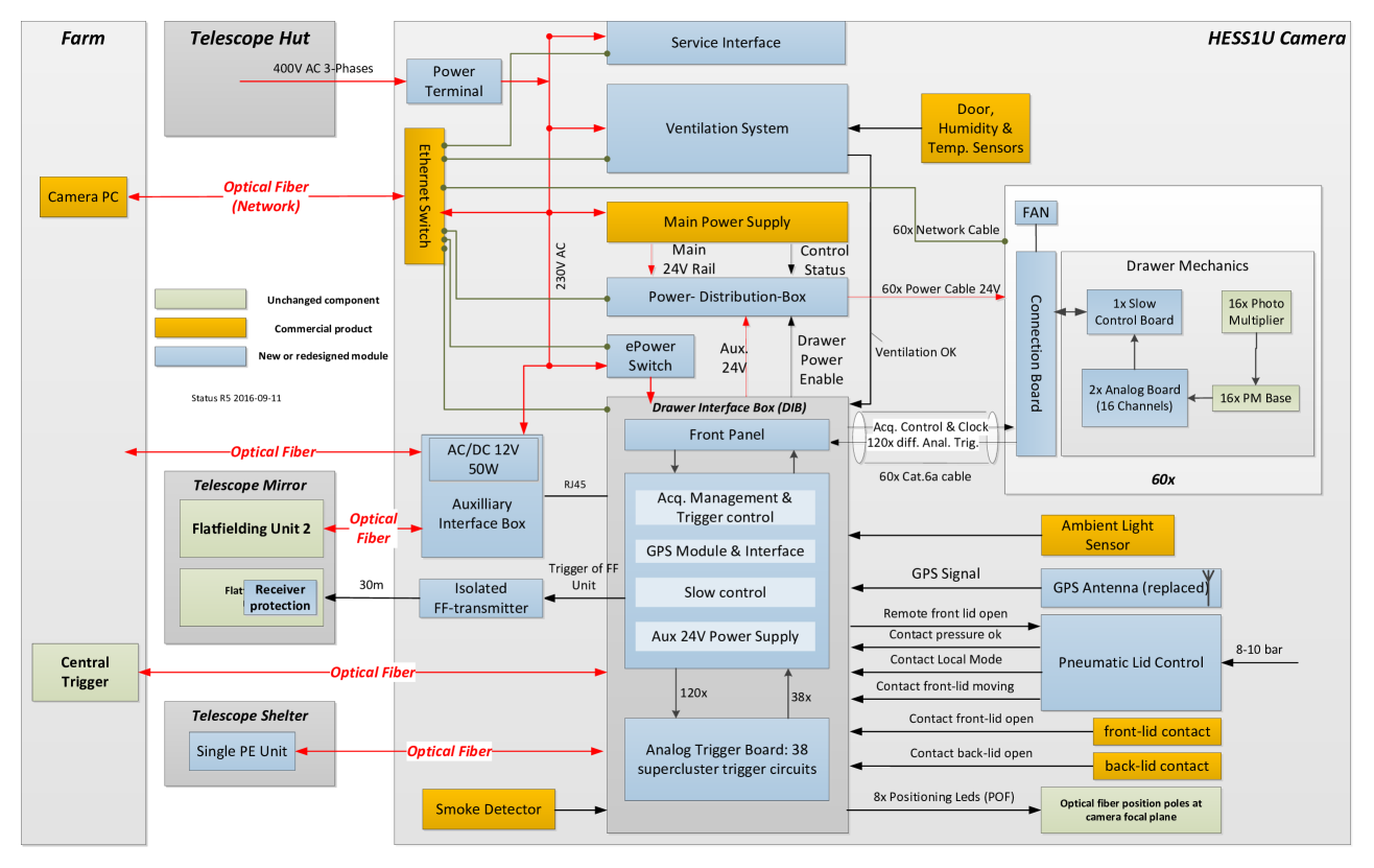
Upgrading the H.E.S.S. I cameras meant replacing or refurbishing essentially every component inside them. Only the photomultiplier tubes (PMTs) and their high voltage power supplies (HV bases) were kept, due to their cost and relative robustness. This can also be seen in the schematic diagram of the camera subsystems (Fig. 2). When possible, commercial off-the-shelf (COTS) solutions were employed. A shared design feature of all custom electronic subsystems developed for the cameras is the usage of an FPGA coupled to a single-board computer, controlled via Ethernet.
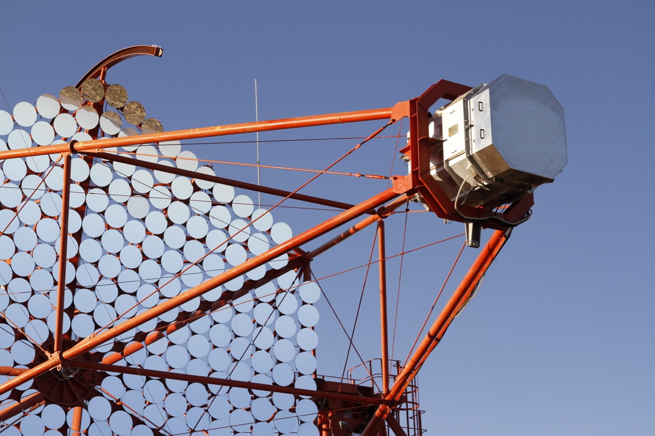
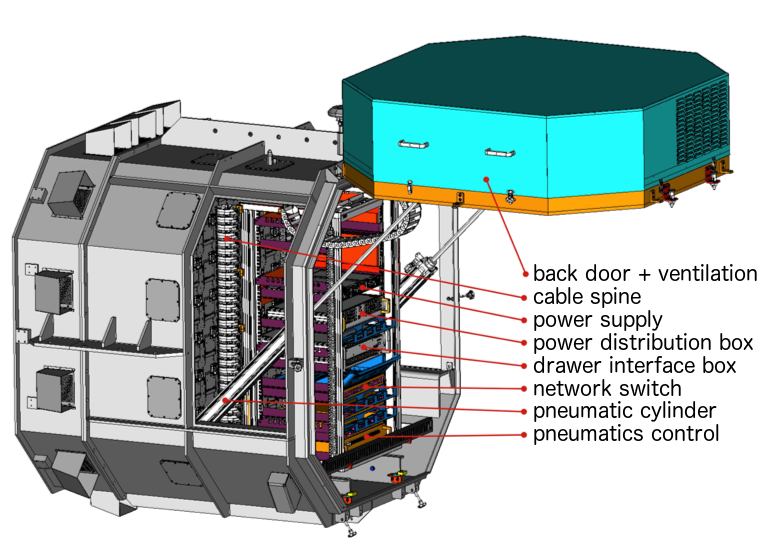
Most of the development, production and testing of the cameras has been done at the DESY site in Zeuthen. A picture of one of the upgraded cameras on the telescope can be seen in Fig. 1, left.
2.1 Front-end electronics
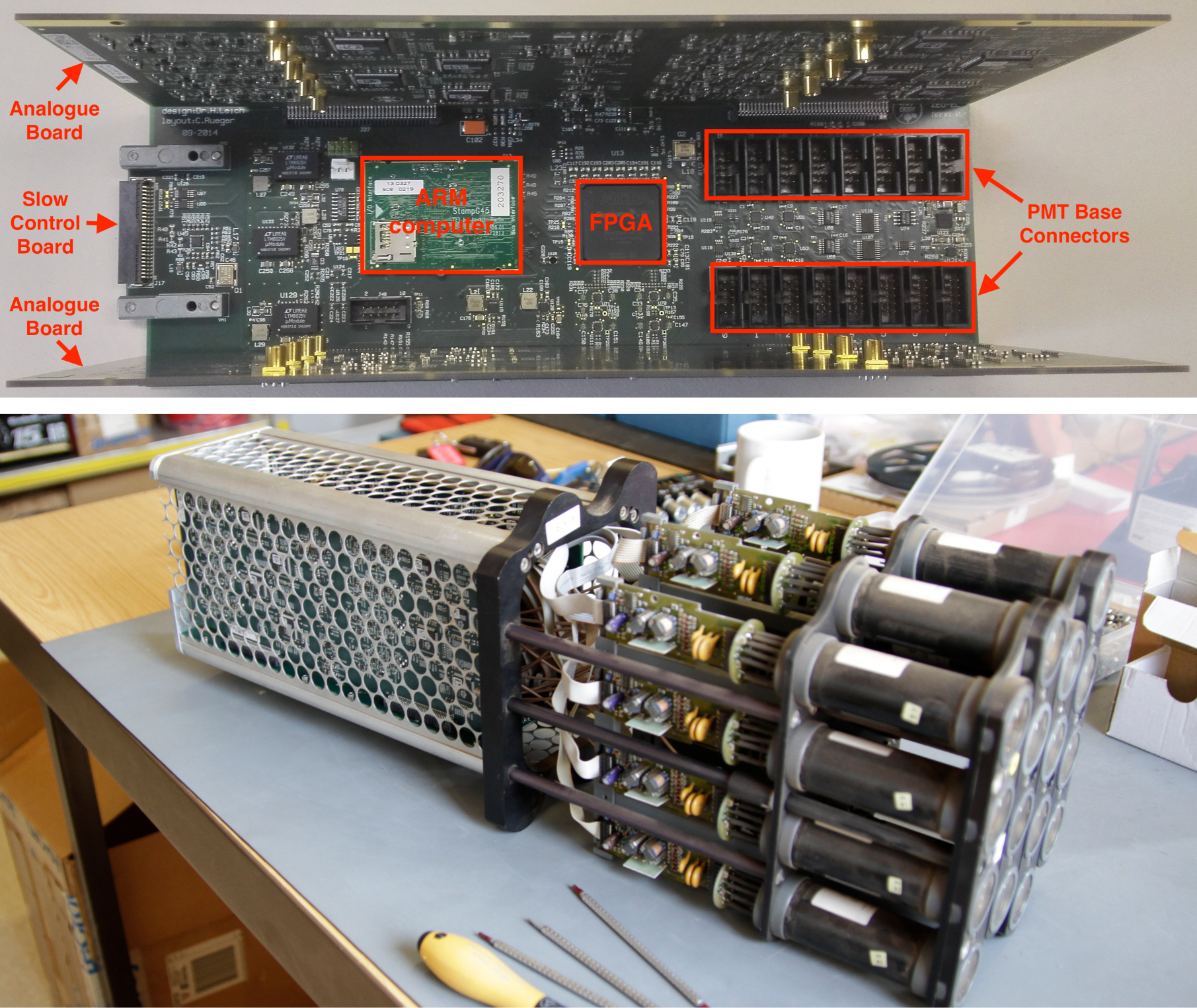
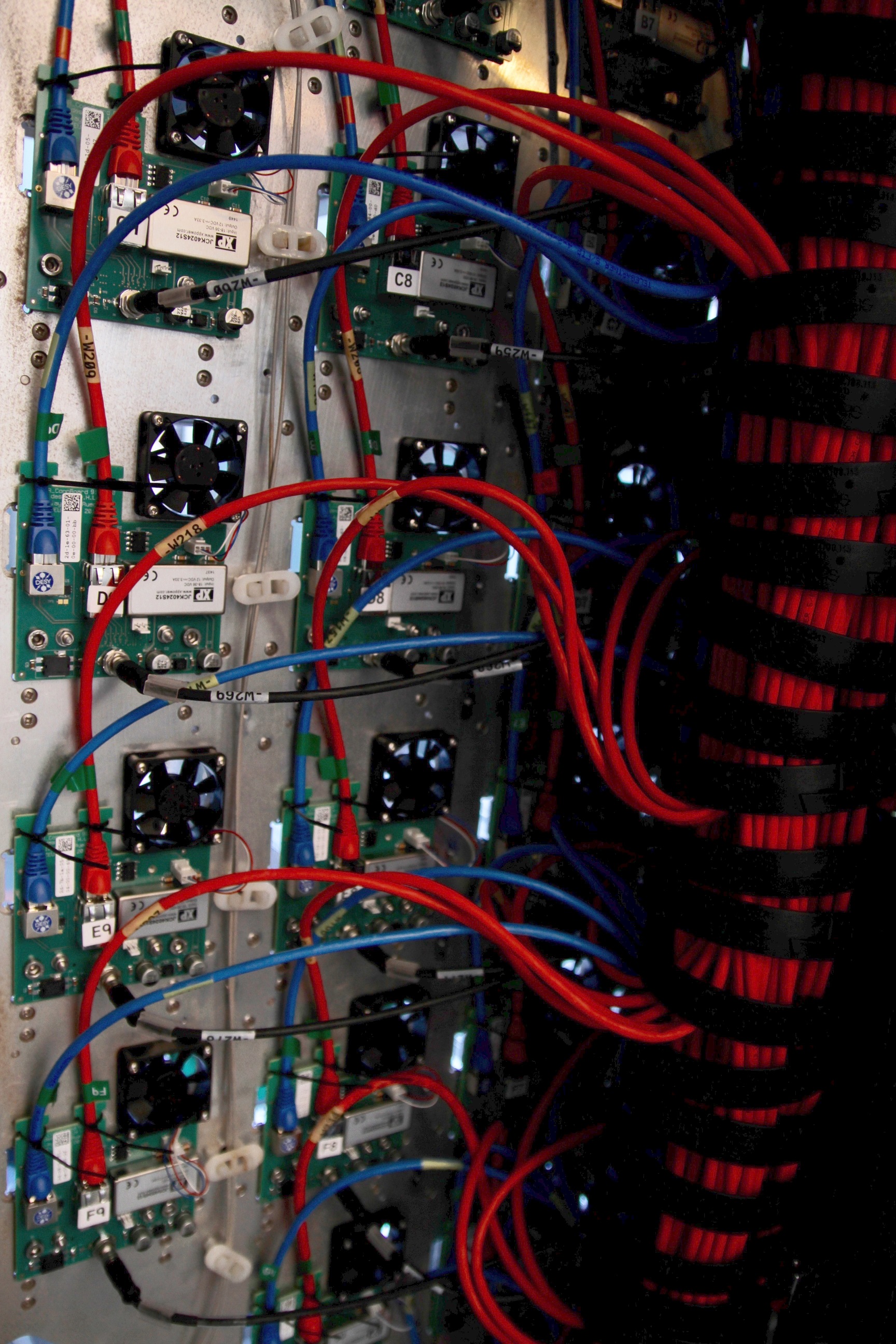
Cherenkov light from particle showers in the atmosphere is detected and digitized in the front-end of the camera. The light sensors are 960 PMTs, organized into 60 modules, called “drawers” (Fig. 3). The drawers are arranged in a rectangular matrix, with each corner of the matrix devoid of 3 drawers. A drawer consists of 16 PMTs, two 8-channel analogue boards, and a slow control board (see Fig. 3, top). The analogue boards host the electronics components responsible for the amplification, discrimination and digitization of the PMT signals (see Fig. 4, left); the slow control board hosts an FPGA (Altera Cyclone IV) controlling the whole drawer, an ARM9-based single-board computer (TaskIt Stamp9G45), the power regulators and the sockets for the PMT HV bases. The drawers are supported by a mechanical structure which separates the front from the back-end of the camera. Each drawer is connected to a connection board secured on the back-end side of that structure, hosting sockets for network, trigger and power (see Fig. 5, right).
2.1.1 Analogue boards
The analogue signal from one PMT is sent to the analogue board via a 15 cm long
coaxial cable. The PMTs produce negative polarity, single-ended voltage pulses
of 2–3 ns duration (FWHM) with an amplitude varying from 1 mV to a few V,
depending on the number of photons detected. Upon reaching the analogue board,
the PMT signals are AC coupled, pre-amplified by a factor 9.8, split into three branches and
further amplified by low noise single-ended to differential amplifiers, which
also invert their polarity.
Two of the branches are routed to the two inputs of
the NECTAr readout chip, for sampling and digitization. Their overall amplification
factors are 15.1 (high gain, HG) and 0.68 (low gain, LG). The NECTAr chip inputs have a nominal range of 2 V, so high gain signals are clipped to 3.3 V, the most convenient voltage
present on the board within the NECTAr chip tolerance range, to avoid affecting the low gain. An adjustable
constant common-mode offset of about 0.2 V is added to the electrical signal to
keep it within the input range even in the case of undershoot (this corresponds
to a pedestal offset of around 420 ADC counts).
The signal in the third branch is amplified by a factor 45 and sent to a
high-speed comparator, whose digital output is directly routed to the FPGA on
the slow control board. This signal is referred to as the level 0 (L0) trigger
signal.
2.1.2 Readout
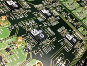
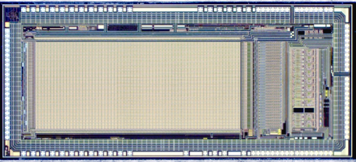
Most of the performance improvements of the upgraded cameras are due to its readout electronics, based on the NECTAr analogue memory chip, designed at CEA/IRFU [5] (Fig. 4, right).
The NECTAr chip has two channels (one per gain), each equipped with a switched capacitor array of 1024 cells, acting as an analogue ring memory buffer. There are two modes of operation: writing and reading. During the writing phase, the input amplitude is stored sequentially on the array capacitors, with a switching frequency of 1 GHz. The writing process is circular over the whole array, so the charge stored in the cells is overwritten every 1024 ns by the new input. A trigger signal stops the writing and initiates the reading: the charges in the capacitor cells of a small region of interest (ROI) are read out and digitized by the on-chip 12-bit 21 Msamples/s ADC. The digital data is then transmitted to an FPGA by means of a serializer. For regular observations the ROI is currently set to 16 cells, and the data in the ROI is summed by the FPGA, and sent to the camera server as one integrated charge value per pixel and per gain. The choice of ROI length and simple summing charge integrator is inherited from the old cameras for compatibility with the existing H.E.S.S. analysis and simulation frameworks (see e.g. [6]). It is a sufficiently adequate choice for most applications since Cherenkov light from atmospheric particle showers reaching the camera has a typical temporal spread of less than 10 ns, except for the most inclined and energetic showers. The performance of the new camera readout and data acquisition systems, however, allows full waveform sampling with an ROI length of up to 48 samples, which is expected to increase the sensitivity of the array to high energy showers. This mode of operation is currently being tested on selected targets, along with more sophisticated charge integration algorithms (see also Sect. 5.3).
2.1.3 Slow Control and Connection boards
The FPGA and ARM computer of each front-end drawer are located on the slow
control board. They are connected via a 100 Mbit/s memory bus, with a 16 bit
word width; the ARM computer has a 100 Mbit/s Ethernet interface and acts as a
device node of the distributed camera control software.
The FPGA reads out sampling data from the NECTAr chip, collects other monitoring
data such as PMT currents and L0 trigger counters, and directly controls all the
electronics inside the drawer. The ARM computer runs a slow control server
accessing the FPGA registers, reads out all FPGA data, buffers it and sends
it over the network to a central camera server via TCP/IP using the ØMQ library [7]. The central camera server controls the drawer by means
of remote procedure calls implemented using the Apache Thrift library
[8].
The drawer slow control board also houses several point-of-load
regulators and DC line filters, providing the required voltage supplies for all
the drawer components. Also, the sockets for the PMT HV bases and the
corresponding control and readout electronics are located at the front-facing
end of the board.
The connection board has 2 RJ45 sockets, one for standard Ethernet and one for four Low Voltage Differential Signaling (LVDS) signals: two trigger outputs, a clock and a readout control input. A 4-pin M8 socket provides 24 V DC (see Sect. 2.2.4) to the main step-down (24 V to 12 V) DC-DC converter, which is also hosted on the connection board. This arrangement assures galvanic isolation of the electronics inside each drawer, preventing ground loops and current surges. It also isolates the rather noisy switching-mode DC-DC converter from the sensitive analog front-end part of the drawer, and allows it to be efficiently cooled. The 12V output of the DC-DC converter is routed to the regulators on the slow control board.
2.2 Back-end electronics
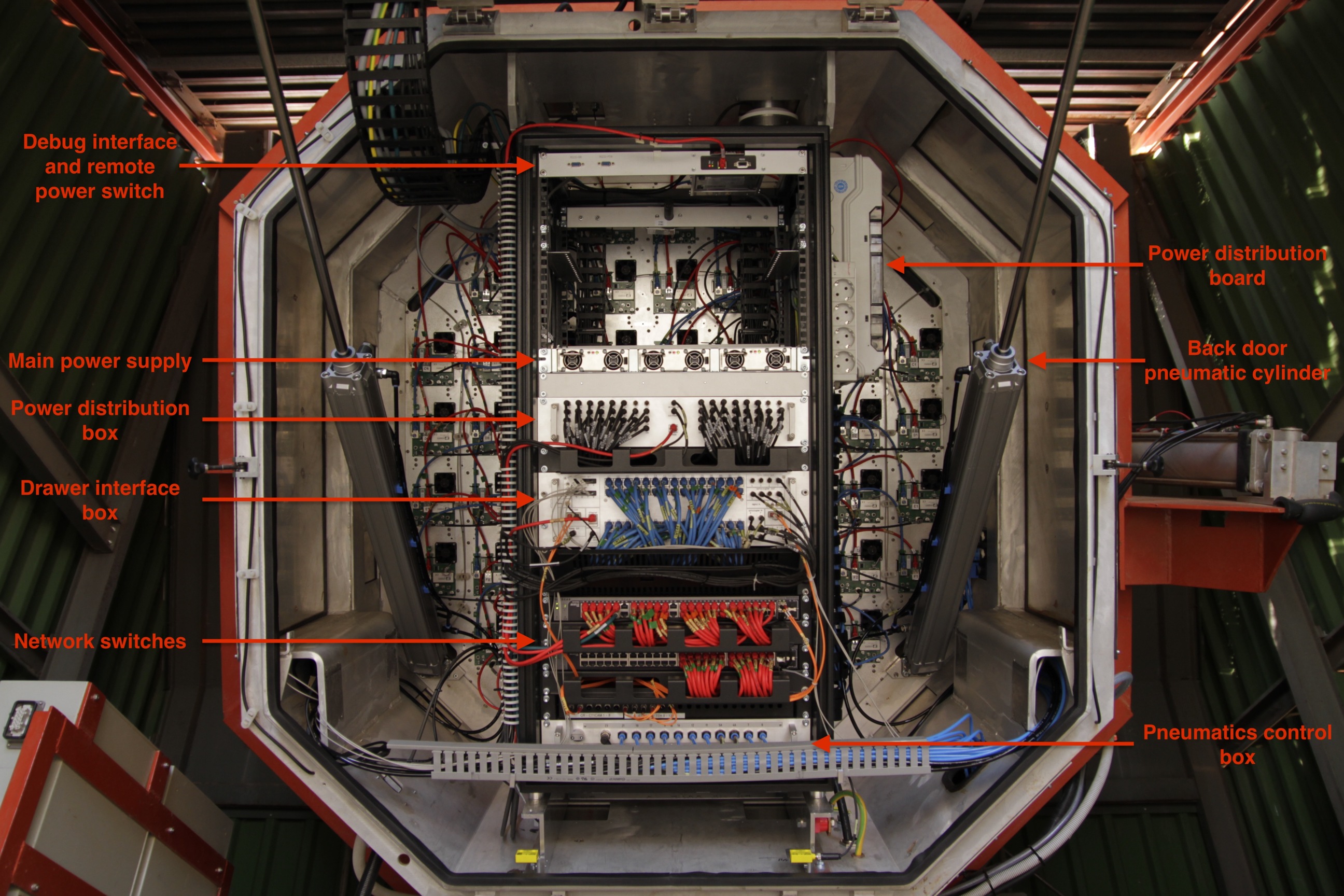
The back-end electronics is deployed inside one 19 inch rack located in the back side of the camera (see Fig. 1, right, and Fig. 5). New components developed specifically for this upgrade are described in the following.
2.2.1 Drawer interface box
The drawer interface box (DIB) is the central hub of the camera. As such, its functions include: trigger and readout control interface and clock distribution to the drawers; camera-level trigger generation; interface to the array central trigger and to the auxiliary camera components, such as the front position LEDs, the pneumatics control and the ambient light sensor (see Fig. 2); GPS timestamping of events and a safety interlock logic to ensure the protection of people, PMTs and camera electronics.
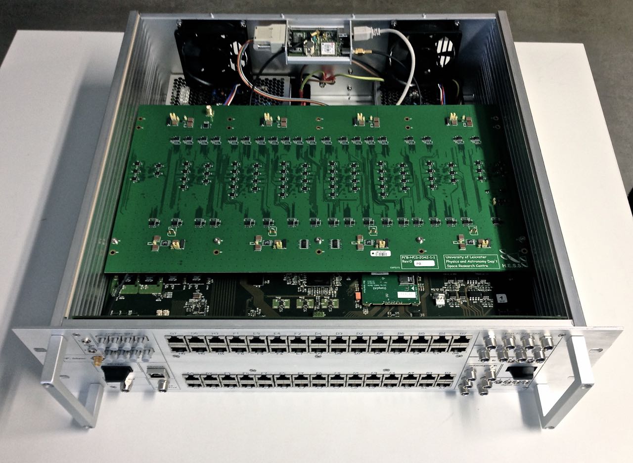
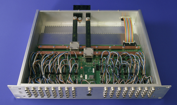
The DIB is composed of three interconnected boards: front panel board, main board and analogue trigger board (see Fig. 6, left). The front panel board houses connectors for the drawer trigger, clock and control signals, the central trigger fiber interface, the front position LEDs lightguides and the other camera sensors and actuators; the main board is where the FPGA and ARM computer are located and all signals are routed; finally the analog board is a mezzanine of the main board, whose purpose is to generate the level-1 (L1) camera trigger (see Sect. 2.2.2).
Furthermore, the DIB is equipped with a GPS module that delivers a pulse-per-second (PPS) signal, to which the main 10 MHz clock, provided by a high precision temperature stabilized quartz oscillator, is disciplined. This clock is also distributed to the drawers. The GPS module also sends a timestamp to the DIB via a serial interface. This is used to timestamp events at the camera level. The precision of the camera GPS timestamp is better than few µs, of the order of the signal transit time between the camera and the central trigger.
2.2.2 Camera trigger and array trigger
The camera trigger architecture is the same as it was in the old camera
electronics, a -majority over “trigger sectors” of 64 contiguous pixels
[9]. Therefore, an -fold coincidence within a sector is
sufficient for the camera to trigger. Usually is set to 3. There are
38 sectors in the camera, which overlap horizontally by one half drawer and
vertically by one full drawer.
This trigger architecture is implemented as follows: the signal from of each PMT
is amplified and compared to a threshold to produce the L0 signal, which is
then routed to the FPGA on the slow control board and sampled there at 800 MHz.
The sampled L0 signal can thus be delayed or stretched in steps of 1.25 ns. Then,
the FPGA counts the number of pixels with an active L0 in each half of the
drawer separately. These two numbers are continuously sent as two LVDS
pulse-amplitude modulated trigger signals to the DIB. The amplitude modulation
has 8 discrete levels with an amplitude of 33 mV each.
In the DIB these amplitude-modulated signals are made single-ended and
isochronally routed to 38 analogue summators, one per sector, located on the
analogue trigger board. Due to the overlapping geometry, each signal is
distributed to up to 4 sector summators. The amplitude of the output of each
summator is proportional to the number of active L0 signals in each sector. This
sector sum signal is then routed to a comparator, where a sector threshold
corresponding to active pixels is applied. All comparator outputs are
subsequently routed to the FPGA of the DIB where they are combined in an OR to
form the camera L1 trigger. When an L1 trigger is present, a length-encoded
“stop” signal is broadcast to all drawers via the LVDS readout control lines,
and an “active” signal is sent to the central array trigger in the control
building via an optical fibre. Upon receiving the “stop” signal, the drawer
FPGA stops the NECTAr writing, and immediately performs the readout and
digitization of the region of interest, storing the data in a front-end buffer.
During regular observations, the H.E.S.S. central trigger [10] sends back an “accept” signal to the CT1–4 cameras only if a coincidence of at least two telescopes “active” signals occurs within an 80 ns window (after correcting for their pointing-dependent light propagation delay). This signal is received by the DIB and forwarded to the drawers, initiating there the storage of the data held in the front-end buffer. Should no “accept” signal arrive, the front-end buffer is discarded after a hold-off time slightly longer than the readout dead-time and the maximum latency of the signal response from the central trigger. If another L1 trigger is issued by the camera before the hold-off is expired, a “busy” signal is sent to the central trigger instead, but no signal is sent to the drawers. “Active”, “accept”, and “busy” triggers share the same fibre connection, so they are pulse-length coded.
A design choice different from the original H.E.S.S. camera trigger, and inspired by the digital camera trigger design for CTA [11] is the 800 MHz sampling of the pixel trigger comparator output (the old logic was asynchronous). One advantage of using a synchronous logic is that the L0 signal can be delayed and stretched, another is the possibility to implement alternative L1 trigger logic architectures. Indeed, two of them have been implemented: a compact next-neighbour (NN, [12]) logic, and a pseudo-analogue sum trigger logic [13]. In both cases no changes in the analogue part of the trigger are made, only the FPGA firmware is different.
In the NN logic, the L1 signal is issued only when a cluster of neighbouring pixels inside a drawer is simultaneously active. In the FPGA this is implemented with a simple look-up table. The implementation however does not take into account NN groups overlapping two drawers.
The pseudo-sum trigger algorithm works by measuring the duration of the L0 signals, instead of just counting the active ones. The idea behind this is that the duration of the L0 signal is proportional to the total charge deposited within the corresponding pixel, because for PMT-like pulses the duration above a certain threshold is proportional to their amplitude (the pulses are roughly triangular, see Fig. 9, left). This measurement is performed in the FPGA for each half-drawer separately, in units of 1.25 ns, within a 5-ns window. The windowing limits the maximum contribution of any L0 signal to 4 counts, and is meant to avoid problems due to PMT after-pulsing similarly to an amplitude clipping. The sum of the duration of the L0 signals of a half-drawer in the preceding 5 ns is transmitted to the analogue trigger board, so the output of any sector summator is proportional to the total charge deposited within the corresponding sector, with an individual pixel clipping given by the windowing.
2.2.3 Ventilation, pneumatic and power systems
The ventilation system consists of a single 250 mm Helios KVW 250/4/50/30 centrifugal fan, two filters in series (coarse and fine) and a 6 kW air heater. The whole system is attached to the back door. When operating, it forces a l/s airflow from the back to the front of the camera, where the outlets are located. The filters ensure that very little dust enters the camera. The heater is turned on automatically if the external humidity is higher than 75%, to prevent condensation, or the external temperature is below 5 ∘C, to minimize temperature gradients across the camera. In operation, the drawer temperature is kept stable at ∘C, with a gradient of ∘C along the top-bottom direction. Both absolute temperature and temperature gradient have no measurable effect on the data and on the trigger efficiency. The internal temperature of the camera is stable for the typical range of external night temperatures, between 0 and 25 ∘C.
The pneumatic system consists of two cylinders for the back door, one cylinder and five clamps for the front lid. Compressed air is provided by an industrial compressor located in the camera shelter. A custom-built pneumatics control box implements a simple control logic using air valves. There are two modes of operation: local or remote. In local mode, all remote operations are inhibited and the front lid and back door can be opened manually using switches on the outside of the camera body. In the default remote mode, only the front lid can be opened and closed using a relay controlled by the DIB. In this mode, a power failure or safety alarm causes the the front lid to close automatically. The status of the pneumatic system is monitored by four sensors: a contact sensor for the back door, two end switches for the front lid, and the remote/local switch. An air horn is blown for a few seconds as a warning before any movement happens.
The camera power is supplied via standard industrial 400 V three-phase AC
mains. Care was taken to ensure that the load was balanced over all three
phases. The ventilation system is directly powered by the mains, while a
distribution board provides 230 V single-phase AC to the network switches, the
front-end power supply, and the DIB. The DIB AC power is remotely controlled by
a commercial network power switch.
The 24 V DC to the drawers is generated by the main front-end power supply, a
commercial TDK-Lambda FPS-S1U unit, equipped with 3 load-sharing FPS1000-24
modules. It is distributed to the drawers by a custom-built power switch called
Power Distribution Box (PDB), see Fig. 6, right. The PDB monitors the
current drawn by each drawer, samples the current and voltage ramps at power-up,
and can shut the drawers off autonomously if it detects an over-current. This
device also employs the FPGA + ARM computer design found elsewhere in the
camera. The power consumption of the whole camera is between 3 and 9 kW,
depending if the air heater is used or not.
2.2.4 Cabling
The cabling uses industry solutions such as standard Ethernet twisted-pair cables wherever possible to ensure ease of procurement and replacement. The data (both readout and slow control) between drawers and backplane is transmitted via TCP/IP over Ethernet by means of standard Cat. 6 cables. The LVDS pulse-amplitude modulated trigger, readout control and 10 MHz clock signals are transmitted on standard Cat. 6A Ethernet cables of equal length (with a tolerance of mm, corresponding to ns). The power is delivered to to each drawer on 4-wire cables terminated with threaded 4-pin M8 connectors. Ethernet and power cables are bundled in special pre-built cable spines (see Fig. 5, right). Auxiliary sensors and actuators are connected using 3-wire or 4-wire electrical cables and standard threaded M8 connectors, except for the GPS antenna which is connected via a standard coaxial cable and SMA connector.
2.3 Auxiliary and calibration devices
Several sensors are deployed inside and outside the camera to monitor door position, temperature, humidity, ambient light and smoke presence. Their signals are fed to a safety interlock system that ensures safe camera operations for both shift crew and hardware. The interlock logic is implemented in the firmware of the DIB FPGA, so it cannot be disabled and is independent of the software implementation.
For the calibration of the gain of the individual PMTs, a device called single
photo-electron (SPE) unit is used. It is located in the shelter, facing the
front of the camera. Due to its position, it can be used only when the
telescope is fully parked. The SPE unit uses an LED to emit pulses
of blue (370 nm) light with pulse frequencies ranging from 38 Hz to 156 kHz.
The intensity of the pulses ranges from to photo-electrons,
and their duration is less than a nanosecond. It was designed at the LPNHE
laboratory in Paris for the original H.E.S.S. array. A plastic diffuser in front
on the LED ensures complete camera illumination, with a uniformity of about 50% [14].
The pulse frequency and intensity are controlled by the camera server via UDP.
An adapter board was added to the SPE unit, allowing it to send its trigger
signal to the camera via an optical fibre connection. This additional trigger
signal is synchronous to the light pulses and it is required for calibration
purposes (see Sect. 4.2).
To perform the pixel-wise calibration of the light collection efficiencies of PMT photo-cathode
and funnels [15], another device called flat-fielding unit is used
[16, 14]. It is located in the centre of
the telescope mirror dish and, similarly to the SPE unit, it has a LED that
emits short ( ns FWHM), blue (390–420 nm) light pulses of fixed intensity
( p.e. at the PMTs). A holographic diffuser is placed in front of it.
The high quality diffuser and the small angle subtended by the camera assure a
uniform illumination. The stability of the flat-fielding intensity and its
non-uniformity across the camera are within 5% RMS.
2.4 Camera network and software
All main subsystems (drawers, DIB, PDB and ventilation system) are connected via
100 Mbit/s Ethernet links to two interconnected 48-port switches located inside
the camera. Their uplink to the main camera server is a 10 Gbit/s optical fibre
connection. The camera server is a commercial 1-unit rack server with a 4-core
Intel Xeon E3-1246v3 processor clocked at 3.5 GHz and 16 GB of DDR3 RAM. It is
housed in the computer “farm” (see Fig. 2), an
air-conditioned server room inside the main control building. The topology of
the internal camera network is star-like: slow-control commands are issued only
by the central camera server, which is also the endpoint of the monitoring,
logging and event data streams. The devices on the network are independent from
one another, and the only access point to the camera is through the camera
server.
This distributed design improves the flexibility and resilence of the camera:
for instance, during data-taking the ARM computer memory (256 MB per module, for
a total of 15.6 GB) is used for buffering the data, preventing data loss during
event bursts.
The software was written from scratch; it has a distributed, multi-architecture nature, as required by the new camera design. Its main functions are slow control and event acquisition; it also includes text-based and web-based user interfaces, extensive unit tests, integration tests and validation routines needed for the mass production, and a full commissioning and calibration suite able to take runs, analyze them and adjust camera parameters independently of the main H.E.S.S. DAQ.
The full codebase is around 100,000 lines of code long, composed by 82% C++, 11% ANSI-C and 7% python. Its implementation was one of the major efforts of the upgrade, and required around 6 man-years by a team composed of two full-time coders and four part-time contributors. This paid off with a 10- to 1,000-fold improvement in speed and reliability over the previous system (see Sect. 5.3 for some performance measurements).
To maximize efficiency, extensibility and maintainability of the codebase, the development team made use of well-tested off-the-shelf open source solutions wherever possible. A single source tree was used for both ARM and x86_64 architectures; cross-compilation was handled by the CMake build system. The operating system running on the ARM computers is the Yocto embedded Linux [17]. It runs a Linux kernel v3.0 patched by the manufacturer, and a custom-built DMA-enabled driver for communicating with the FPGA. The remote procedure call framework required to control the camera is implemented using the Apache Thrift library. The camera slow control software was interfaced to the already existing H.E.S.S. data acquisition software (DAQ, [18]) via the CORBA protocol. Data transfer is accomplished via the ØMQ [7] smart socket library. The raw data serialization protocol is custom, and optimized for speed; for monitoring and logging the general-purpose Google Protocol Buffers library [19] is used instead.
3 Test facilities and procedures
The development of a new detector generally requires planning and implementing test and verification procedures. The testing needs of H.E.S.S. I Upgrade cameras were identified early on in the project and grouped into four main stages (prototyping, integration, quality control, commissioning), for which four distinct test facilities were build, and are described in the following.
3.1 Table-top laboratory test bench
During the prototyping stage daily debugging and testing of the prototypes was
needed to validate the design of the new electronics and the correct
implementation of all features needed. These mostly manual and one-time
characterization tests required a versatile laboratory test setup.
For this purpose, a table-top laboratory test bench was set up, equipped with
an oscilloscope (LeCroy DPO 4104), an arbitrary function generator
(Agilent 81160A), and several auxiliary instrumentation such as a variable
attenuator and a digital multimeter. Many results shown here, such as the
linearity shown in Fig. 13, left or the bandwidth shown in
Fig. 12, right, have been obtained using this setup.
When the mass production of 270 drawers started, each one of them had to
undergo more than 300 individual tests to pass the quality control. The tests
mainly checked the functionality of the drawer, but also included the
calibration of the NECTAr chip; and the characterization of readout noise,
linearity, saturation, cross-talk.
The table-top test bench was thus refitted with four purpose-built,
Ethernet-controlled 8-channel pulse generators, allowing to perfom the
above-mentioned tests automatically. The generators are built using the same
FPGA-ARM computer combination used elsewhere and were seamlessly integrated in
the test software. They deliver PMT-like pulses with fast ( ns) rising
and falling edges, variable amplitude (from 0.6 - 300 mV), delay (0 - 64 ns in
steps of 0.25 ns) and width (2-62 ns in steps of 0.25 ns). They have a RJ45
socket to provide the LVDS drawer clock and acquisition control signal, and to
test the outgoing drawer trigger signals; an external trigger input, output and
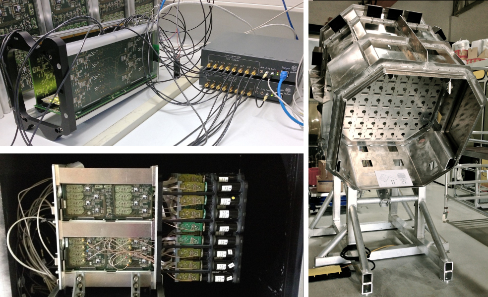
gate, which allow them to be daisy-chained, see Fig. 7, top left.
Two daisy-chained generators can simultaneously test all 16 channels of one
drawer: during the quality control, the test bench could therefore test two
drawers in parallel.
Using this setup, running all the tests needed for quality control of a drawer
took less than 30 minutes. Several of these tests only use self-contained
testing functionalities of the drawer, such as the possibility of inject fake
pulses at the PMT signal inputs to test the trigger path. Such tests can
therefore be run even when the drawer is not on the test bench: during the
commissioning of the cameras, they proved to be an invaluable troubleshooting
tool.
3.2 Single drawer black box test bench
The integration of the new front-end electronics with the existing H.E.S.S. I PMTs
was a critical step, and it required a setup to test a PMT-equipped drawer with
a low level of background illumination, with the possibility of flashing it with
Cherenkov-like light pulses.
A single-drawer “black box” test bench was built for this purpose. It
consists of a simple aluminium box holding a complete drawer. A H.E.S.S. I SPE
unit is used to illuminate the PMTs and is attached to the side of the box
facing them. The inside of the box is painted black to minimize reflections.
The black box was used extensively during the first stages of prototyping, and
later on to devise the appropriate calibration routines. After prototyping was
over, it was shipped to the H.E.S.S. site, where it was used during the
deployment of the cameras, mostly to inspect malfunctioning drawers during the
day. It is still being used on site occasionally for drawer maintenance and
refitting.
3.3 Mini-camera
The verification tests needed during the integration and commissioning phases called for a fully functional camera. A 4-drawer “mini-camera” was built for this purpose (Fig. 7, bottom left), housed in a 1 m3 light-tight enclosure, with 64 PMTs, one DIB and a light source (an SPE unit). With it, it was possible to test the integration between front-end and back-end by recreating a minimal 1-sector trigger setup. This allowed testing the analogue trigger board and the other trigger functionalities of the DIB using realistic signals, as close to the field conditions as possible. The mini-camera was also used to develop and test the slow control and event builder software and to test their integration into the existing H.E.S.S. DAQ control software.
After the installation of the first telescope, the mini-camera served as the main commissioning test bench. In fact, it became the primary way of reproducing and troubleshooting in the laboratory problems found during the first months of field operations.
3.4 Full camera copy
Later in the project, the camera on-site assembly and integration had to be prepared and rehearsed as thoroughly as possible before actual deployment. This stage required a full camera, so a copy of the camera body was fabricated at the LLR laboratory and installed at DESY Zeuthen (Fig. 7, right). Due to its size, it could not be housed in a light-tight room, so the PMTs were not used, but all other components of all four cameras were mounted and tested first on this camera body, with the purpose of verifying their functionality and training the technicians involved in the assembly. Thanks to this, the on-site physical assembly of one camera could be finished in less than 5 working days. In 2015, the total down-time of the CT1 telescope, excluding commissioning and fine-tuning, was 18 days. In 2016, the CT2-4 telescopes had a total down-time of four weeks.
Other testing and validation activities performed on the copy camera included checks of the cable mapping; full trigger chain functionality check; assessment of the event builder performance and its integration with the H.E.S.S. software; configuration of the camera-internal network; evaluation of the capabilities of ventilation system, slow control software, and power supply; mechanical integration of the new back door and the pneumatic system.
4 Camera calibration
The following section is an overview of the calibration procedures needed to commission the upgraded cameras, partly updating the information found in [14].
4.1 Readout
4.1.1 Nectar line correction
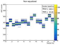
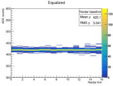
The NECTAr switched capacitor array is arranged in 16 lines 64 columns of analogue storage cells. The analogue input is buffered by amplifiers providing the signal for each of the 16 lines. Since each line has its own input buffer and readout amplifier, a spread of the DC baseline levels between lines is observed. This dispersion is stable in time and can be compensated by DC line offsets regulated by 16 integrated digital to analogue converters (DACs). In order to calibrate their values, sample-wise pedestal runs are taken with a readout width of at least 16 samples, and the average difference between the sample baselines and a reference default value (defined as 420 ADC counts to reserve roughly 10% of the dynamic range for pulse undershoots) are calculated. The line offset DAC settings can thus be corrected to compensate this difference. By repeating this process several times, the default baseline offset is approached. In only 5 iterations, the RMS of the baseline decreases from to ADC counts on average, see Fig. 8. This procedure needs to be performed in principle only once, but in practice it is performed for the whole camera each time a drawer is exchanged, or the PMT gain is re-adjusted, so about twice per year on average. The values of the line DACs are then permanently stored in a MySQL database. This correction is not strictly necessary for regular observations, where the only measured quantity is the charge integrated over 16 samples, minus a time-averaged pedestal baseline. This is because the width of the ROI is a multiple of the line dispersion period, so any event-wise baseline shift due to it is cancelled out.
4.1.2 Readout window adjustment
The NECTAr chips continuously store signals inside their analogue memory ring
buffers until the arrival of an L1 trigger signal. When this happens, the
region of interest is located cells before the last sampled one, where
is the L1 trigger latency in nanoseconds. It is therefore necessary to measure
the trigger latency for each chip and trigger source. This is done by
illuminating the whole camera with high intensity ( p.e.) reference
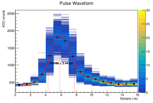
light pulse (see e.g. Fig. 9, left) while varying the NECTAr register controlling the start of the region of interest inside the chip
buffer, until the sampled pulse signal is located at the center of it. Since
the chip buffer is 1024 cells deep and circular, is the complementary of
over the buffer length, .
The position of the readout window needs to be adjusted individually for two
trigger sources having different latencies: the SPE unit trigger and the
standard camera level 1 trigger. For the former, the SPE unit itself provides
the reference light pulses; for the latter the flat-fielding unit is used.
After a successful adjustment, the two sets of values are stored in a
MySQL database.
4.2 PMT gain flat-fielding
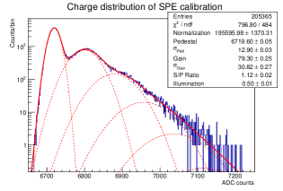
In order to reliably measure the amount of light arriving at the camera, it is necessary to equalize the gain of the electronic chain of each channel. This is done by varying the voltage applied to the PMTs, and illuminating the camera with pulses from the SPE unit, at an intensity so low that the average number of photons detected by a PMT for each light pulse is less than 1. The typical charge distribution of these calibration runs can be seen in Fig. 9, right. The charge is integrated over the standard 16 ns ROI. This distribution can be fit by a linear combination of Gaussian functions, as shown in [14], equation 6. This simple fit form is quite robust over a wide range of PMT illuminations (0.1–3 p.e.), but its result is biased: the actual PMT single photo-electron charge distribution is not a Gaussian, but an asymmetric distribution skewed towards lower values. So, the average single photo-electron amplitude is lower than the amplitude at the peak, as shown in [20]. This discrepancy is corrected later on in the analysis by a factor 0.855 derived from realistic simulation of the H.E.S.S. I PMTs [21]. After this correction, the systematic error in determining the PMT gain has been estimated with simulations to be within %. Other techinques for the single photo-electron calibration, such as those described in [22, 23], are currently being evaluated.
Similarly to their predecessors, the PMT gain of H.E.S.S. I upgrade cameras is flat-fielded to a conversion factor of 80 ADC counts (peak value obtained from the above-mentioned fit). This particular value is chosen empirically, based on the reproducibility and robustness of the fit results. The corresponding average PMT gain is . The PMT voltages range from V up to 1,350 V, and are stored in a MySQL database. To achieve a precise gain flat-fielding (better than 4%), the procedure is iterated several times, each with a finer voltage step. The performance of the PMTs degrade with time, so their gains need to be flat-fielded every six months, adding on average 13 V to the PMT voltages. After gain flat-fielding, the position of the region of interest is readjusted, because the PMT transit time depends on the voltage applied to it.
4.3 Camera flat-fielding
After equalizing the PMT gains, to correctly estimate the amount of Cherenkov light reaching the detector plane, one needs to calibrate the differences in light collection efficiency for each pixel. As mentioned previously, this is achieved by recording light flashes generated by the flat-fielding unit. In fact, assuming the flat-fielding light is homogeneous, one can easily calculate a correction factor from the charge recorded by each pixel and its average over all camera pixels : . This is done for the high and low gain channels separately. Flat-fielding runs are also used to calibrate the time of maximum information of each pixel, under the assumption that the flat-fielding pulses arrive isochronally at their entrance window. The flat-fielding is performed several times per observation period (one lunar month), and the obtained coefficients for the period are then averaged and stored in a MySQL database. As for the previous cameras, the distribution of the coefficients is a Gaussian with an RMS of 10%, there is no discernible gradient across the camera. Trials with a new flat-fielding unit are ongoing.
4.4 Trigger
As described in section 2.2.2, the camera trigger has several parameters which require dedicated calibrations. The most important ones are the pixel and sector thresholds and , and the pixel L0 delay . The L0 stretching is set to zero to have a trigger response similar to the one of the old cameras. Central trigger delays also have to be adjusted after the installation of a camera.
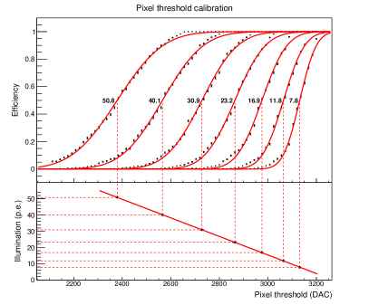
Calibrating the pixel threshold requires finding the relationship between its value as set by the electronics, in DAC counts, or mV, and its effective value in photoelectrons. This is done with special calibration runs, where a variable-intensity pulsed light source is needed. The SPE unit is used for this purpose. The camera is flashed with a fixed frequency and an varying intensity , between and p.e. The light pulse intensity in each pixel is measured from the mean of its charge distribution using a previously-determined PMT gain coefficient. While the run is ongoing, is varied and the L0 pixel trigger efficiencies are measured as the ratio between the pixel trigger rate and . The resulting graph is a sigmoid, whose mid-point marks the value of needed to discriminate photoelectrons (see figure 10, left). By repeating this procedure for several intensities, it is possible to determine the offset and slope of the linear dependency , and thus the effective value of in photoelectrons.
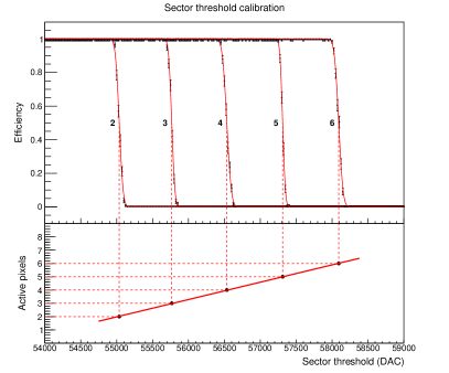
The calibration of , the sector threshold, is likewise accomplished by means of special flat-fielding runs. With the flat-fielding unit activated at a frequency , one enables pixels in every sector, varies and measures the sector trigger efficiency as ratio between the measured sector trigger rate and . The mid-point of the resulting sigmoid curve corresponds to the value of the threshold for the given (see figure 10, right). Since is discrete, this sigmoid is much steeper than the one for . By repeating this procedure for several values of , it is possible to determine the relationship in a similar way as for the pixel threshold. Finally, for the nominal multiplicity of 3, is set to a value for which all sectors have 100% efficiency when and 0% when .
The L0 delays calibration is much simpler: using a modified drawer FPGA firmware, it is possible to send the sampled L0 information of all pixels on the data stream. This is done while flashing the camera with the flat-fielding unit, so all pixels are illuminated at the same time. The L0 delays are then individually adjusted until the rising edge of all L0 signals is aligned.
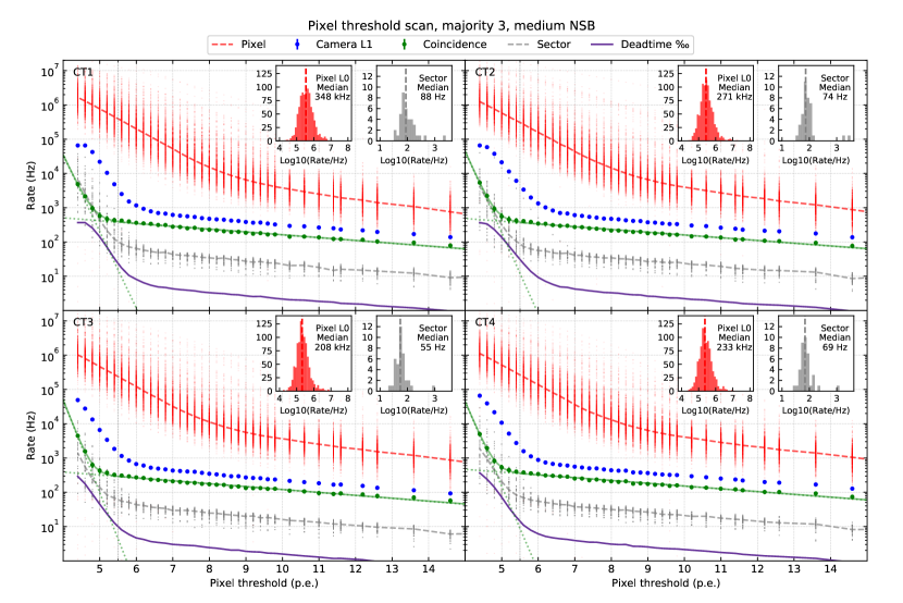
After the above-mentioned calibrations, it is necessary to determine the operating point of . To do that, is varied while measuring the camera L1 and coincidence trigger rates during a regular observation run. This “threshold scan” is performed under optimal observing conditions, using the whole array, including CT5. It results in “bias curves” for all four telescopes, shown in Fig. 11. In these plots, the steeply falling part of the coincidence rate at thresholds lower than p.e. is due to noise from the night sky background (NSB) light, whereas the flatter part at higher threshold values is due to cosmic-ray showers. These two components can be fit by two exponential functions, and the value of is conservatively chosen so that coincident events due to noise are less than 1% of all triggers. For regular camera operation, is 5.5 p.e., which ensures stable operation even at higher levels of NSB light, up to MHz photon rate. Note that at this value of , the single-telescope L2 trigger rates are already in the noise, with rates well in excess of 1 kHz, which with the old cameras would have caused more than 36% of the events to be lost due to dead-time, a figure that becomes around with the new cameras, thanks to the new NECTAr-based readout.
At the array level, it is important to measure the signal round-trip time between the central trigger and the camera, in order to adjust the fixed part of the central trigger coincidence delays, which also vary depending on the pointing direction. This is done by sending a trigger signal via optical fiber from the central trigger to the DIB, which then replies to it. The difference between the time of sending and that of receiving is measured at the central trigger with an oscilloscope. On average, the round-trip time was reduced by ns with respect to the original cameras.
5 Performance
We report some of the most significant performance metrics for the new Cherenkov cameras in this section. Some of them were measured in the lab, prior to the installation of the cameras, others in the field in Namibia, during or after commissioning.
Efforts are ongoing to fully characterize the performance of the new cameras in terms of gamma-ray sensitivity using simulations and standard candle data; and to exploit the several new features they offer. The results will be made available in upcoming publications by the H.E.S.S. collaboration.
5.1 Analogue front-end
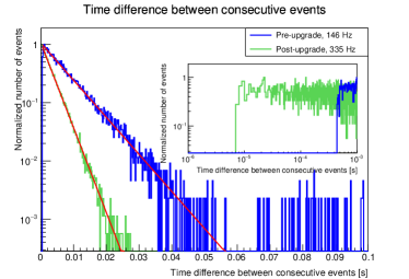
The dead-time of a NECTAr chip when reading the nominal 16 cells region of interest is about µs [25, 26]. However, the minimum safe time interval between two events is greater than the nominal dead-time of the NECTAr chip, because of the trigger signal generation and the chip readout process on the FPGA take µs. Also, for the version of the NECTAr chip used here, the first 16 readout cells have to be read out and discarded because of stale values, adding another µs to the dead-time. Due to all this, the hold-off time is set to: ns, where is the total number of NECTAr cells read out ( for regular observations). This can be appreciated in Fig. 12, left, which shows that the overall dead-time of the upgraded H.E.S.S. I cameras, measured from the distribution of the time difference of two consecutive events during a regular observation run is µs.
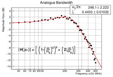
The nominal analogue bandwidth of the NECTAr chip is 410 MHz [25, 26]. The design of the analogue electronics uses components matching or exceeding that bandwidth. The end-to-end -3 dB bandwidth of the readout is MHz, more than four times higher than in the previous camera, see Fig. 12, right. One can see the benefit of such a high bandwidth in the sampled PMT pulse shape shown in the left panel of Fig. 9, where the FWHM is less than 3.5 ns. Such narrow peaks allow a better determination of shower time profiles, which can be used to improve the sensitivity of the analysis [27, 28].
The design of the analogue part of the readout was optimized for low noise. The pedestal noise, which is the RMS of the value of a single NECTAr cell in the presence of no input signal is on average ADC counts, or mV. This corresponds to the pure electronic noise of the front-end. For the typical PMT gain of , and charge integration window of 16 samples, the electronic noise of front-end and PMT combined has on average a RMS of ADC counts, or photo-electrons (p.e.). This is measured routinely during single photo-electron calibration runs, as the RMS value of the pedestal distribution (see Fig. 9, right). The noise intensity varies with the position of the channels inside the drawer: the channels whose amplifiers are physically located in the front of the drawer, closer to the PMTs (channels 4–7 and 12–15) have higher electronic noise ( p.e. RMS) than the ones who are in the back of the drawer ( p.e. RMS), forming two distinct populations. This is likely due to different noise pick-up along the routes of the traces on the analog circuit board. It is anyway not a problem because at the chosen gain, the single-electron signal is distinguishable in any case, being always at least 3 times higher than the noise.
The linearity and cross-talk of the readout were measured by recording a pre-calibrated, PMT-like pulse of variable intensity. The results, which can be seen in the left panel of Fig. 13, show that non-linearities in both high gain and low gain amount to less than 2%. The linear range of the high gain is 0.3–200 p.e. and that of the low gain is 30–4,200 p.e.: the total readout dynamic range is greater than 80 dB. The ratio between high and low gain is between 30 and 200 p.e. (see Fig. 13, left, bottom panel).
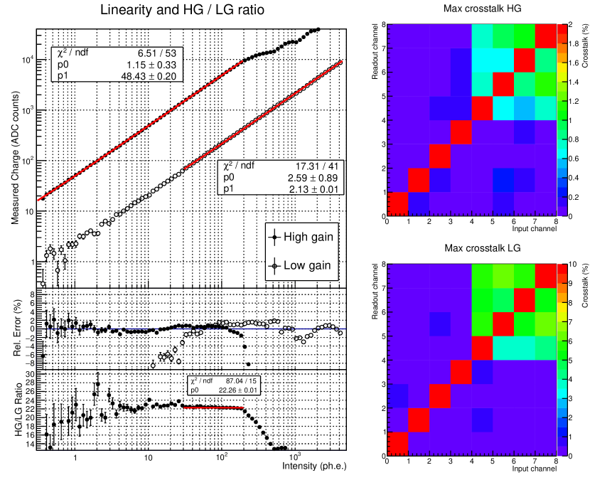
The data mentioned above was also used to characterize the cross-talk between two channels on the same analogue board. For the high gain channel the cross-talk is typically less than 0.5%, and never larger than 1%; for the low gain is at most 7% (see Fig. 13, right). It is measured using the largest PMT-like pulse inside the linear range of each gain, and taking the ratio between the charge recorded in an empty channel () to that measured in the input channel (). Similarly to the electronic noise, the cross-talk is also larger for the front channels (4–7 and 12–15) than for the back ones. This problem was studied in detail with auto-correlation and frequency domain analysis of the recorded noise, but no obvious cause was found [29].
5.2 Trigger
The optimization of the trigger described in the previous section increased the fraction of events triggered stereoscopically with CT5 by more than a factor of two. Before the upgrade it was 20%, after the upgrade it is 44%. This is a direct consequence of the reduced deadtime of the camera due to the NECTAr chip, which allows the camera pixel threshold to be lowered substantially.
In the case of observations with a low NSB light intensity in the field of view (i.e. an average pixel photon rate across the camera of less than 100 MHz), the nominal pixel trigger threshold can be lowered by 1 p.e, to 4.5 p.e. Preliminary studies on simulations showed that this simple adjustment results in marginal improvements in terms of threshold trigger effective area, which were not deemed sufficient to justify the manpower investment in the production and maintenance of a full new set of simulations and instrument response functions.
The next-neighbour alternative trigger architecture was also tested and simulated, but it was found not to deliver a substantially improved performance with respect to the default 3-majority scheme. The performance of the pseudo-sum trigger alternative is still under study due to the higher number of parameters to optimize and difficulty of implementing a realistic simulation.
5.3 Readout and slow control
The NECTAr chip design, the modularity of the camera, the advanced driver for
the FPGA–ARM memory bus exploiting direct memory access (DMA) technology and
the ample software buffering allow for a maximum achievable data acquisition
rate with default settings (i.e. readout and storage of integral charge and
timing information) of around 10 kHz per telescope. This is about twenty times higher than
the usual CT1–4 acquisition rate during regular observations. It was
determined by field tests under realistic conditions.
The bottleneck is the
transfer of data to the H.E.S.S. main DAQ program, because the network bandwidth
is only 1 Gb/s. Performance tests on a 10 Gb/s network showed that the cameras
could sustain a constant individual data acquisition rate in excess of 50 kHz. The system can sustain short bursts of events at a much higher rate by buffering the data in the RAM of the ARM computer and of the camera server. This can be very important for some
physics cases, such as transient events and especially GRBs.
The improvement of the new camera readout system allows to configure the readout so that full waveforms of up to 48 samples are stored alongside the integrated charge over 16 ns and the timing information. This is expected to be beneficial in the reconstruction of inclined or large impact parameter showers with energies larger than 1 TeV, for which the arrival time dispersion of Cherenkov light at the telescope is greater than 16 ns. This readout mode increases the amount of transmitted data by a factor (each drawer sends 51 data blocks instead of the usual 3). In order to keep up with the usual data acquisition rates (up to 700 Hz) when using this acquisition mode, the additional waveform data must be stored on the camera server hard disks, and is transmitted to the H.E.S.S. DAQ off-line on the following day. This mode is only used for selected targets, due to the much greater amount of data created when it is active. Initial results on the performance of this readout mode are reported in [30].
Regarding the slow control software performance, stress tests performed on the Apache Thrift RPC framework operating in the busy DESY lab network showed that it is capable of sustaining rates of 10,000 single point-to-point request/replies per second for more than 12 hours with no failures. One-to-many requests, such as distributing a command or collecting information from all drawers, are handled on the camera server by spawning one thread per connection. This strategy allows for a command distribution latency of ms.
5.4 Commissioning and long-term stability
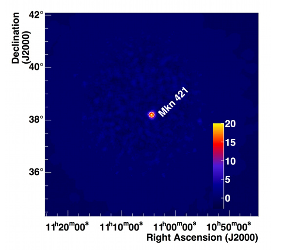
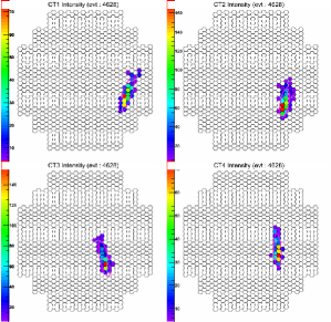
The upgrade of the first camera, that of CT1, was carried out in July/August 2015. This was followed by an extended integration and commissioning period of 9 months. During this period of time, many bugs and problems were ironed out, while the rest of the array (CT2-5) continued scientific observations with minimally degraded performance. This strategy allowed us to compare old and new cameras after the first one was completely commissioned. The other three upgraded cameras were installed in September/October 2016 and underwent a much shorter commissioning phase of four months. In January 2017, a bright flare from the well-known Mkn 421 blazar was observed by H.E.S.S. using the new upgraded cameras, following an alert reported by the HAWC collaboration [31]. About 2 hours of data were collected during this observation. The preliminary processing of the data using two independent analysis pipelines revealed a clear detection with a significance of 16. This was the first detection of a TeV gamma-ray source using the NECTAr chip technology [32] (see Fig. 14, for a significance sky map of this detection and an example event). The upgraded cameras have been employed in routine observations since January 2017, and since then have achieved an average weather-corrected data taking efficiency of 98.5%.
6 Conclusion
The four upgraded cameras of the 12-meter H.E.S.S. Cherenkov telescopes were successfully deployed on site in 2015 and 2016. They are equipped with a new NECTAr-based readout technology that substantially reduces the dead-time by a factor of 60 from µs in the previous system to µs in the new cameras. Furthermore, the new design allows for a more robust, versatile and efficient operation and maintenance, leading to improved performance and reliability. All components of the cameras were tested, integrated and calibrated, and their performance was validated in the field. The camera configuration was optimized, resulting in more than twice the amount of stereoscopically recorded showers by the H.E.S.S. array.
The achieved average data taking efficiency of the cameras is 98.5%. No major problems due to ageing were found during an ordinary maintenance campaign that took place in early 2019. Thus, all the primary goals of the project have been achieved.
In addition, the new cameras offer the possibility of using more sophisticated and flexible trigger and readout algorithms. The most promising of these new possibilities is to record fully sampled waveforms, which is being explored intensively in current observation campaigns and will be reported on in the future.
The new cameras are foreseen to be in use in the H.E.S.S. experiment for its remaining lifetime.
References
References
- Aharonian et al. [2006] F. Aharonian, et al., Observations of the Crab Nebula with H.E.S.S., Astronomy and Astrophysics 457 (2006) 899.
- Bolmont et al. [2014] J. Bolmont, et al., The camera of the fifth H.E.S.S. telescope. Part I: System description, Nuclear Instruments and Methods in Physics Research Section A: Accelerators, Spectrometers, Detectors and Associated Equipment 761 (2014) 46–57.
- Delagnes et al. [2006] E. Delagnes, Y. Degerli, P. Goret, P. Nayman, F. Toussenel, P. Vincent, SAM: A new GHz sampling ASIC for the H.E.S.S.-II front-end electronics, Nuclear Instruments and Methods in Physics Research Section A: Accelerators, Spectrometers, Detectors and Associated Equipment 567 (2006) 21–26.
- Vincent et al. [2003] P. Vincent, et al., Performance of the H.E.S.S. cameras, in: Proceedings, 28th International Cosmic Ray Conference (ICRC 2003), Tsukuba, Japan, 31 Jul - 7 Aug 2003, volume 5, Universal Academy Press, pp. 2887–2890.
- Naumann et al. [2012] C. L. Naumann, et al., New electronics for the Cherenkov Telescope Array (NECTAr), Nuclear Instruments and Methods in Physics Research Section A: Accelerators, Spectrometers, Detectors and Associated Equipment 695 (2012) 44.
- de Naurois and Rolland [2009] M. de Naurois, L. Rolland, A high performance likelihood reconstruction of -rays for imaging atmospheric Cherenkov telescopes, Astroparticle Physics 32 (2009) 231 – 252.
- zmq [2019] Code Connected - zeromq, https://zeromq.org/, 2019. Accessed: 2019-07-02.
- apa [2019] Apache Thrift - Home, https://thrift.apache.org/, 2019. Accessed: 2019-07-02.
- Rolland [2005] L. Rolland, Calibration of the cameras of the H.E.S.S. gamma-ray experiment and observations of the Galactic Centre above 100 GeV, Ph.D. thesis, Université Pierre et Marie Curie - Paris VI, 2005.
- Funk et al. [2004] S. Funk, et al., The trigger system of the H.E.S.S. telescope array, Astroparticle Physics 22 (2004) 285–296.
- Wischnewski et al. [????] R. Wischnewski, U. Schwanke, M. Shayduk, Performance study of a digital camera trigger for CTA, in: Proceedings, 32nd International Cosmic Ray Conference (ICRC 2011): Beijing, China, August 11-18, 2011, volume 9, p. 63.
- Bulian et al. [1998] N. Bulian, et al., Characteristics of the multi-telescope coincidence trigger of the HEGRA IACT system, Astroparticle Physics 8 (1998) 223 – 233.
- Rissi et al. [2009] M. Rissi, N. Otte, T. Schweizer, M. Shayduk, A New Sum Trigger to Provide a Lower Energy Threshold for the MAGIC Telescope, IEEE Transactions on Nuclear Science 56 (2009) 3840 –3843.
- Aharonian et al. [2004] F. Aharonian, et al., Calibration of cameras of the H.E.S.S. detector, Astroparticle Physics 22 (2004) 109–125.
- K. Bernlöhr and others [2003] K. Bernlöhr and others, The optical system of the H.E.S.S. imaging atmospheric Cherenkov telescopes. Part I: layout and components of the system, Astroparticle Physics 20 (2003) 111 – 128.
- Aye et al. [2003] K.-M. Aye, et al., A Novel Alternative to UV-Lasers Used in Flat-Fielding VHE g-Ray Telescopes, in: Proceedings, 28th International Cosmic Ray Conference (ICRC 2003), Tsukuba, Japan, 31 Jul - 7 Aug 2003, volume 5, p. 2975.
- yoc [2019] Yocto Project | Open Source embedded Linux build system, package metadata and SDK generator, https://www.yoctoproject.org/, 2019. Accessed: 2019-07-02.
- Balzer et al. [2014] A. Balzer, et al., The H.E.S.S. central data acquisition system, Astroparticle Physics 54 (2014) 67.
- pro [2019] Protocol Buffers, https://developers.google.com/protocol-buffers, 2019. Accessed: 2019-07-02.
- Bernlöhr [2008] K. Bernlöhr, Simulation of imaging atmospheric Cherenkov telescopes with CORSIKA and sim_telarray, Astroparticle Physics 30 (2008) 149–158.
- K. Bernlöhr [2002] K. Bernlöhr, CORSIKA and sim_hessarray mc simulation of the imaging atmospheric cherenkov technique for the H.E.S.S. experiment, H.E.S.S. Internal Note, 2002. 02/04.
- Saldanha et al. [2017] R. Saldanha, L. Grandi, Y. Guardincerri, T. Wester, Model Independent Approach to the Single Photoelectron Calibration of Photomultiplier Tubes, Nuclear Instruments and Methods in Physics Research Section A: Accelerators, Spectrometers, Detectors and Associated Equipment 863 (2017) 35–46.
- Takahashi et al. [2018] M. Takahashi, et al., A technique for estimating the absolute gain of a photomultiplier tube, Nuclear Instruments and Methods in Physics Research Section A: Accelerators, Spectrometers, Detectors and Associated Equipment 894 (2018) 1–7.
- Casadei [2012] D. Casadei, Estimating the selection efficiency, Journal of Instrumentation 7 (2012) P08021.
- Delagnes et al. [2011] E. Delagnes, et al., NECTAr0, a new high speed digitizer ASIC for the Cherenkov Telescope Array, in: 2011 IEEE Nuclear Science Symposium Conference Record, pp. 1457–1462.
- Delagnes [2016] E. Delagnes, Specifications of the NECTAr0 Chip, Internal Document Irfu CEA Saclay, 2016. V.4 2016-01-05.
- Aliu et al. [2009] E. Aliu, et al., Improving the performance of the single-dish Cherenkov telescope MAGIC through the use of signal timing, Astroparticle Physics 30 (2009) 293 – 305.
- Stamatescu et al. [2011] V. Stamatescu, et al., Timing analysis techniques at large core distances for multi-TeV gamma ray astronomy, Astroparticle Physics 34 (2011) 886 – 896.
- Shiningayamwe [2017] K. P. Shiningayamwe, Investigating electronic pedestals of the analoque front-end boards of the upgraded high-energy stereoscopic system (H.E.S.S. I) cameras, Thesis, University of Namibia, 2017.
- Zorn [2019] J. Zorn, Sensitivity Improvements of Very-High-Energy Gamma-Ray Detection with the Upgraded H.E.S.S. I Cameras using Full Waveform Processing, in: Proceedings, 36th International Cosmic Ray Conference (ICRC 2019), Madison, WI, U.S.A., 24 Jul - 1 Aug 2019, volume ICRC2019, Proceedings of Science, p. 834.
- Martinez et al. [2017] I. Martinez, J. Wood, R. Lauer, HAWC detection of further increase in TeV gamma-ray flux from Mrk 421, The Astronomer’s Telegram 9946 (2017).
- SOM [2017] H.E.S.S. Collaboration - Source of the Month - March 2017, https://www.mpi-hd.mpg.de/hfm/HESS/pages/home/som/2017/03/, 2017.
Acknowledgements
The support of the Namibian authorities and of the University of Namibia in facilitating the construction and operation of H.E.S.S. is gratefully acknowledged, as is the support by the German Ministry for Education and Research (BMBF), the Max Planck Society, the German Research Foundation (DFG), the French Ministry for Research, the CNRS-IN2P3 and the Astroparticle Interdisciplinary Programme of the CNRS, the U.K. Science and Technology Facilities Council (STFC), the IPNP of the Charles University, the Czech Science Foundation, the Polish Ministry of Science and Higher Education, the South African Department of Science and Technology and National Research Foundation, and by the University of Namibia. We appreciate the excellent work of the technical support staff in Zeuthen, Durham, Hamburg, Heidelberg, Palaiseau, Paris, Saclay, and in Namibia in the construction and operation of the equipment.
The authors would also like to thank the anonymous reviewers for their valuable insights.