Quantum device fine-tuning using unsupervised embedding learning
Abstract
Quantum devices with a large number of gate electrodes allow for precise control of device parameters. This capability is hard to fully exploit due to the complex dependence of these parameters on applied gate voltages. We experimentally demonstrate an algorithm capable of fine-tuning several device parameters at once. The algorithm acquires a measurement and assigns it a score using a variational auto-encoder. Gate voltage settings are set to optimise this score in real-time in an unsupervised fashion. We report fine-tuning times of a double quantum dot device within approximately 40 min.
I Introduction
Electrostatically defined semiconductor quantum dots are intensively studied for solid-state quantum computation Loss and DiVincenzo (1998); Kloeffel and Loss (2013); Hanson et al. (2007); Vandersypen et al. (2017). Gate electrodes in these device architectures are designed to separately control electrochemical potentials and tunnel barriers Camenzind et al. (2018, 2019). However, these device parameters vary non-monotonically and not always predictably with applied gate voltages, making device tuning a complex and time consuming task. Fully automated device tuning will be essential for the scalability of semiconductor qubit circuits.
Tuning of electrostatically defined quantum dot devices can be divided into three stages. The first stage consists of setting gate voltages to create the confinement potential for electrons or holes. In our laboratory, full automation of this stage has been achieved as reported in Ref. Moon et al. (2020). The second stage, known as coarse tuning, focuses on identifying and navigating different operating regimes of a quantum dot device. Automated coarse tuning has been demonstrated using convolutional neural networks to identify the double quantum dot regime Zwolak et al. (2019) and reach arbitrary charge states Durrer et al. (2019). Template matching was also used to navigate to the single-electron regime Baart et al. (2016). During this stage, virtual gate electrodes can be used to independently control the electrochemical potential of each quantum dot Mills et al. (2019); Volk et al. (2019). The third stage, referred to as fine-tuning, involves optimising a particular set of charge transitions. Previous work on automated fine-tuning focused on optimising the tunnel coupling between two quantum dots by systematically modifying gate voltages until this coupling converges to a target value Van Diepen et al. (2018); Teske et al. (2019). However, these approaches are restricted to a few device parameters and rely on calibration measurements.
Here, we demonstrate an automated approach for simultaneous fine-tuning of multiple device parameters, such as tunnel rates and inter-dot tunnel coupling. Our approach is based on a variational auto-encoder (VAE). In particular, we focus on double quantum dot devices. Electron transport through these devices is typically presented as a charge stability diagram, displaying the current flowing through the device as a function of two gate voltages. Bias triangles are regions in the stability diagram, for which current flow is allowed through a double quantum dot device under a bias voltage van der Wiel et al. (2002), and reveal most of the device parameters. Our algorithm aims at optimising various bias triangle characteristics commonly associated with favourable device parameters, as done by humans when tuning these devices. The VAE compresses training data displaying bias triangles to a lower-dimensional space, called the latent or embedding space. In this latent space, a human expert identifies target locations corresponding to bias triangles in the training set which exhibit favourable transport characteristics. The algorithm acquires a measurement displaying bias triangles and assigns to these bias triangles a location in latent space. The distance between this location and the chosen target locations is used by the algorithm as a basis to score the measurement, and this score is used to optimise the gate voltage settings in real time.
We have previously shown that VAEs signifcantly improve the efficiency of quantum dot measurements Lennon et al. (2019). We have now, for the first time, used a VAE to fine-tune a double quantum dot device by locally optimising transport features in a completely automated manner. Without requiring any prior knowledge of the device architecture, we are able to fine-tune several device parameters at once.
II Device and overview of the algorithm
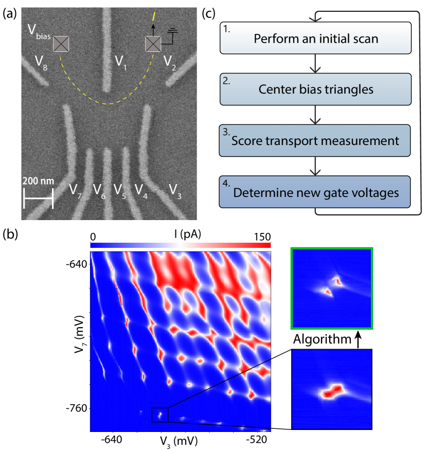
We demonstrated our fine-tuning algorithm on a lithographically defined double quantum dot device. The device comprises a GaAs/AlGaAs heterostructure confining a two-dimensional electron gas (2DEG). Quantum dots are defined by Ti/Au gate electrodes which are patterned on top of the heterostructure (Fig. 1a). DC voltages to are applied to these gate electrodes. A bias voltage determines the flow of current through the device. A stability diagram for our double quantum dot device is shown in Fig. 1b. All measurements were performed at approximately mK. The stability diagram exhibits bias triangles, which reveal device parameters such as charging energies, tunnel coupling to the left and right electrodes and inter-dot tunnel coupling. The shape, sharpness and brightness of bias triangles are related to those device parameters and are thus used to guide device tuning.
Our algorithm follows a similar approach to device tuning by humans. It consists of four major steps (Fig. 1c). In each iteration, an initial low resolution stability diagram is acquired to center a pair of bias triangles. Next, a high resolution measurement of the bias triangles is performed and scored by the VAE. Based on this score, the set of gate voltages is determined for the next iteration.
III VAE implementation
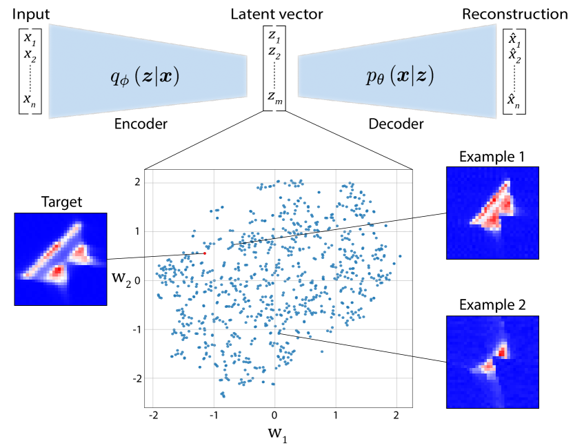
The VAE consists of an encoder and decoder, both embodied in neural networks Kingma and Welling (2014). The encoder maps input data to a low-dimensional latent vector which is real-valued. The decoder maps a latent vector to a reconstruction . The parameters of the encoder and the decoder neural networks are and , respectively. The VAE is a generative model; it seeks to preserve the maximum amount of information during the encoding process so that input data can be reconstructed with minimal error during the decoding process. During a training phase, and are iteratively updated to minimize a loss function. The loss function is given by a reconstruction error , which penalises the networks for producing reconstructions that are dissimilar from the input data, and a regularisation term , which enforces input data with similar characteristics to be encoded in close proximity in latent space. The reconstruction error and the regularisation term have weights and , respectively.
We implement Factor-VAE Kim and Mnih (2018), an adaption of VAE that seeks to generate a latent space in which each dimension corresponds to a unique characteristic of the input data. The Factor-VAE framework assumes that there are underlying independent factors associated with the data. If fully disentangled, each of those factors can be identified with a dimension in latent space. By using a Factor-VAE, we aim to generate a latent space in which each dimension is associated with a single bias triangle characteristic, such as size or brightness. In this way, the distance in latent space to a target location results in a good metric to score acquired measurements.
The loss function of Factor-VAE includes a total correlation term which encourages the distribution of embeddings to be disentangled. It is given by:
| (1) |
where the total correlation term is given by , i.e. the Kullback-Leibler divergence between the distribution of embeddings and the product of the distribution of embedding components , with the index corresponding to the th latent space dimension. The total correlation loss term has a weight . Since this term is intractable, it is estimated using a discriminator . The discriminator is trained to classify between non-factorial and factorial samples, i.e. that its input is a sample from rather than from .
The training set for the Factor-VAE was collected from a device which differs considerably in material, architecture and transport regime from the device used to demonstrate the performance of the algorithm, evidencing its generality. The VAE was trained using 2253 sets of bias triangles, measured on a double quantum dot defined in a Ge/Si core-shell nanowire Camenzind (2019); Froning et al. (2018). In order to increase the robustness of the VAE, simple data augmentation techniques were applied. Data augmentation included translation, rotation, mirroring, Gaussian noise and random contrast, resulting in a total training set of 8732 stability diagrams of pixel resolution 32 x 32. The dimension of the latent space was set to 10, as in Ref. Kim and Mnih (2018), given the similar structure of input data. We tried multiple combinations of weights , and to achieve the optimal VAE performance, which was found emperically for , and .
IV Score metric
The score metric used by the algorithm is given by the distance between the latent space representation of an input stability diagram and the latent space representation of a set of target inputs. Note that the loss function is used during training, while the score metric is used for optimisation. A measurement acquired by the algorithm is assigned a low (high) VAE score if its representation in latent space is near to (far from) the targets in latent space. Embeddings that are close together in latent space have similar , implying that the original inputs can be generated using similar underlying variables. As a result, bias triangles that are assigned a low score possess similar characteristics to the target bias triangles.
The target bias triangles are chosen from the unaugmented training set by a human expert who recognises in these triangles the characteristics indicative of favourable quantum dot parameters. The targets are augmented using the same augmentation techniques as described in III. Augmentation of 30 selected targets resulted in a total target set of size 360.
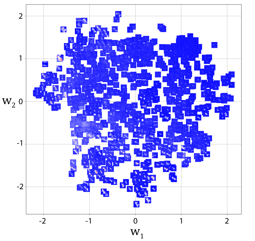
In Fig. 2 the latent space of the trained VAE is shown, and the embedding locations of example target and training inputs are indicated. A full plot of the latent space of the trained VAE with original input stability diagrams is shown in the Supplementary Material.
To write the expression for the score , where denotes the th input measurement, we use the latent vector produced by the encoder for this measurement. The output of the encoder is assumed to follow a multivariate Gaussian with diagonal covariance structure: , where the mean and variance are outputs of the encoding network. Considering two independent normal distributions in latent space, the expectation value of the squared distance between the distributions is given by:
| (2) |
For each input measurement embedded in latent space , (2) is used to determine the distance in latent space to target input . The final score consists of the average of the distance to its nearest targets:
| (3) |
where is the set of targets closest to in latent space. In this way, optimal tuning corresponds to a low score. We found that for , the score metric produced a robust ranking of the training inputs in terms of their similarity to the targets.
V Optimisation
The optimisation starts from the device tuned to the double quantum dot regime so that at least one pair of bias triangles is identified, for which we used the algorithm presented in Moon et al. (2020). After acquiring the initial low resolution stability diagram, the bias triangles are centered using Laplacian of Gaussian (LoG) blob detection. In computer vision, blob detection techniques aim to detect bright regions on dark backgrounds or vice versa Lindeberg (1993). In Fig. 1b, the two examples of bias triangles displayed were centered with this novel approach. Once the triangles are centered, the high resolution scan (32 x 32 pixels, 17 x 17 mV) is acquired and evaluated using the VAE distance score metric. Based on the outcome value of , a decision model sets the gate voltage configuration for the next stability diagram measurement. This process is iterated until the bias triangles are optimised in terms of characteristics such as shape, sharpness and brightness.
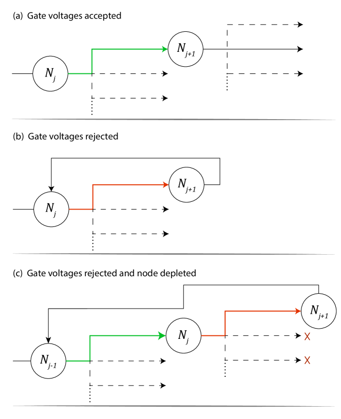
The decision model for proposing gate voltage configurations is illustrated in Fig. 3. Node represents the set of gate voltages applied by the algorithm. In each iteration, one gate electrode is selected at random, and the voltage applied to this electrode is modified by a fixed amount . Therefore, the algorithm chooses between a number of branches equal to twice the number of gate electrodes to be tuned. We chose mV based on human experience in tuning similar devices. After centering and acquiring a high resolution measurement of the resulting bias triangles, the value of determines the algorithm’s decision. If is lower than the previously best (lowest) scored bias triangles, the gate voltage change is accepted, leading to a new gate voltage configuration . Conversely, if is higher, the gate voltage change is rejected and the gate voltage setting returns to its previous configuration. In this case, the rejected gate voltage change will be an excluded branch in the random selection corresponding to the next iteration. Branches that lead to the reversal of the latest accepted gate voltage change are excluded too. It is possible that all gate voltage branches become depleted, in which case the decision model returns to the previously accepted gate voltage configuration with unexplored branches.
VI Experimental demonstration
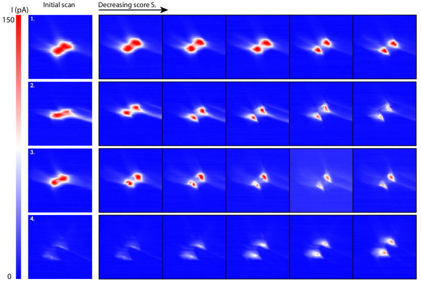
We test the algorithm for different bias triangles measured on our device. Stability diagrams are measured as a function of barrier gate voltages and , which are adjusted during centering of the bias triangles. The gate voltages optimised by the algorithm are , and . For simplicity, we chose to keep gate voltages , and fixed. We checked their effect on the optimised bias triangles was weak. All measured stability diagrams are min-max normalised with respect to the stability diagram obtained after the initial tuning to the double quantum dot regime. In Fig. 4, the optimisation of four different pair of bias triangles is shown.
In cases 1 to 3, the initial bias triangles lack a well-defined shape, indicative of small inter-dot tunnel coupling van der Wiel et al. (2002). Furthermore, pronounced co-tunnelling lines, which are denotative of second-order transport processes, are observed. As the optimisation progresses, the bias triangles separate from each other and acquire a sharper triangular shape. Also, co-tunnelling currents are reduced. In the fourth case, the initial stability diagram shows very faint bias triangles. The optimisation algorithm proves capable of increasing the current flowing through the double quantum dot while preserving most of the other bias triangle characteristics. More examples of bias triangle optimisations achieved by our algorithm can be found in the Supplementary Material.
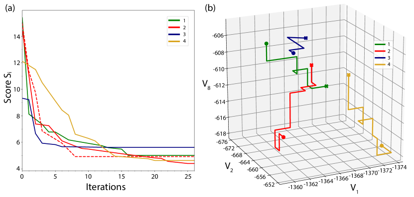
Fig. 5a shows as a function of the number of iterations of our algorithm for cases 1 to 4. Most of the optimisation takes place during the first ten iterations, after which the score does not change significantly. In all cases, the algorithm completes the optimisation within 26 iterations, corresponding to a total tuning time of 36 min. This time is limited by the measurement time, which could be drastically reduced by radio-frequency reflectometry techniques Petersson et al. (2010); Ares et al. (2016); Schupp et al. (2018); Barthel et al. (2009); Pakkiam et al. (2018); West et al. (2019); Urdampilleta et al. (2019); Zheng et al. (2019).
In Fig. 5b we plot the trajectories in gate voltage space corresponding to each optimisation case. The average distance in gate voltage space between the initial gate voltage configurations is greater than for the final gate voltage configurations. This suggests that there exists a region in gate voltage space for which the bias triangles exhibit the most favourable transport characteristics, regardless of their values of and . Additional data can be found in the Supplementary Material.
VII Conclusion
We experimentally demonstrate an optimisation algorithm for the fine-tuning of bias triangles in gate-defined quantum dots. The algorithm scores real-time measurements by computing distances in the embedding space of a VAE. We show that this score can be used to locally optimise double quantum dot parameters in a completely automated manner. No prior knowledge of the device is required and the algorithm proves capable of tuning multiple device parameters at once.
The robustness and efficiency of the decision model could potentially be improved by using Bayesian optimisation or reinforcement learning for proposing new voltage configurations and minimising the score. Also, while we utilised the Euclidean distance between two Gaussian distributions for computing scores, recent work argues that the decoder induces a Riemannian metric in the latent space Arvanitidis et al. (2018). This would imply that shortest paths in latent space do not correspond to straight lines. Therefore, it might prove insightful to implement a Riemannian metric to measure latent space distances. Finally, the influence of selecting targets with different characteristics, such as different excited state energies, could be investigated in the future.
While all measurements presented are performed on a gate-defined GaAs double quantum dot, the VAE was trained on data obtained from a Ge/Si core-shell nanowire device, showing the algorithm is readily applicable to different types of devices. Moreover, our algorithm can be adapted to include any number of additional gate electrodes, paving the way for the tuning of quantum dot arrays.
Acknowledgements.
We acknowledge discussions with E. A. Laird. This work was supported by the Royal Society, the EPSRC National Quantum Technology Hub in Networked Quantum Information Technology (EP/M013243/1), the Quantum Technology Capital grant (EP/N014995/1), Nokia, Lockheed Martin, the Swiss NSF Project 179024, the Swiss Nanoscience Institute and the EU H2020 European Microkelvin Platform EMP grant No. 824109. This publication was also made possible through support from Templeton World Charity Foundation and John Templeton Foundation. The opinions expressed in this publication are those of the authors and do not necessarily reflect the views of the Templeton Foundations. We acknowledge J. Zimmerman and A. C. Gossard for the growth of the AlGaAs/GaAs heterostructure. Lastly, we acknowledge F.N.M. Froning and F.R. Braakman for providing the Ge/Si training data.References
- Loss and DiVincenzo (1998) D. Loss and D. P. DiVincenzo, “Quantum computation with quantum dots”, Phys. Rev. A 57, 120–126 (1998).
- Kloeffel and Loss (2013) C. Kloeffel and D. Loss, “Prospects for spin-based quantum computing in quantum dots”, Annual Review of Condensed Matter Physics 4, 51–81 (2013).
- Hanson et al. (2007) R. Hanson, L. P. Kouwenhoven, J. R. Petta, S. Tarucha, and L. M. K. Vandersypen, “Spins in few-electron quantum dots”, Reviews of Modern Physics 79, 1217–1265 (2007).
- Vandersypen et al. (2017) L. M. K. Vandersypen, H. Bluhm, J. S. Clarke, A. S. Dzurak, R. Ishihara, A. Morello, D. J. Reilly, L. R. Schreiber, and M. Veldhorst, “Interfacing spin qubits in quantum dots and donors-hot, dense, and coherent”, npj Quantum Information 3 (2017).
- Camenzind et al. (2018) L. C. Camenzind, L. Yu, P. Stano, J. D. Zimmerman, A. C. Gossard, D. Loss, and D. M. Zumbühl, “Hyperfine-phonon spin relaxation in a single-electron GaAs quantum dot”, Nature Communications 9 (2018).
- Camenzind et al. (2019) L. C. Camenzind, L. Yu, P. Stano, J. D. Zimmerman, A. C. Gossard, D. Loss, and D. M. Zumbühl, “Spectroscopy of quantum dot orbitals with in-plane magnetic fields”, Phys. Rev. Lett. 122, 207701 (2019).
- Moon et al. (2020) H. Moon, D. T. Lennon, J. Kirkpatrick, N. M. van Esbroeck, L. C. Camenzind, L. Yu, F. Vigneau, D. M. Zumbühl, G. A. D. Briggs, M. A. Osborne, D. Sejdinovic, E. A. Laird, and N. Ares, “Machine learning enables completely automatic tuning of a quantum device faster than human experts”, arXiv:2001.02589 .
- Zwolak et al. (2019) J. P. Zwolak, T. McJunkin, S. S. Kalantre, J. P. Dodson, E. R. MacQuarrie, D. E. Savage, M. G. Lagally, S. N. Coppersmith, M. A. Eriksson, and J. M. Taylor, “Auto-tuning of double dot devices in situ with machine learning”, arXiv:1909.08030 .
- Durrer et al. (2019) R. Durrer, B. Kratochwil, J. V. Koski, A. J. Landig, C. Reichl, W. Wegscheider, T. Ihn, and E. Greplova, “Automated tuning of double quantum dots into specific charge states using neural networks”, arXiv:1912.02777 .
- Baart et al. (2016) T. A. Baart, P. T. Eendebak, C. Reichl, W. Wegscheider, and L. M. K. Vandersypen, “Computer-automated tuning of semiconductor double quantum dots into the single-electron regime”, Applied Physics Letters 108 (2016).
- Mills et al. (2019) A. R. Mills, D. M. Zajac, M. J. Gullans, F. J. Schupp, T. M. Hazard, and J. R. Petta, “Shuttling a single charge across a one-dimensional array of silicon quantum dots”, Nature Communications 10 (2019).
- Volk et al. (2019) C. Volk, A. M. J. Zwerver, U. Mukhopadhyay, P. T. Eendebak, C. J. van Diepen, J. P. Dehollain, T. Hensgens, T. Fujita, C. Reichl, W. Wegscheider, and L. M. K. Vandersypen, “Loading a quantum-dot based ”Qubyte” register”, npj Quantum Information 5 (2019).
- Van Diepen et al. (2018) C. J. Van Diepen, P. T. Eendebak, B. T. Buijtendorp, U. Mukhopadhyay, T. Fujita, C. Reichl, W. Wegscheider, and L. M. K. Vandersypen, “Automated tuning of inter-dot tunnel coupling in double quantum dots”, Applied Physics Letters 113 (2018).
- Teske et al. (2019) J. D. Teske, S. S. Humpohl, R. Otten, P. Bethke, P. Cerfontaine, J. Dedden, A. Ludwig, A. D. Wieck, and H. Bluhm, “A machine learning approach for automated fine-tuning of semiconductor spin qubits”, Applied Physics Letters 114 (2019).
- van der Wiel et al. (2002) W. G. van der Wiel, S. De Franceschi, J. M. Elzerman, T. Fujisawa, S. Tarucha, and L. P. Kouwenhoven, “Electron transport through double quantum dots”, Rev. Mod. Phys. 75 (2002).
- Lennon et al. (2019) D. T. Lennon, H. Moon, L. C. Camenzind, L. Yu, D. M. Zumbühl, G. A. D. Briggs, M. A. Osborne, E. A. Laird, and N. Ares, “Efficiently measuring a quantum device using machine learning”, npj Quantum Information 5 (2019).
- Kingma and Welling (2014) D. P. Kingma and M. Welling, “Auto-Encoding Variational Bayes”, ICLR 2014 (2014).
- Kim and Mnih (2018) H. Kim and A. Mnih, “Disentangling by factorising”, 35th International Conference on Machine Learning, ICML 2018 6, 4153–4171 (2018).
- Camenzind (2019) L. C. Camenzind, Spins and orbits in semiconductor quantum dots, Ph.D. thesis, University of Basel (2019).
- Froning et al. (2018) F. N. M. Froning, M. K. Rehmann, J. Ridderbos, M. Brauns, F. A. Zwanenburg, A. Li, E. P. A. M. Bakkers, D. M. Zumbühl, and F. R. Braakman, “Single, double, and triple quantum dots in Ge/Si nanowires”, Applied Physics Letters 113, 073102 (2018).
- van der Maaten and Hinton (2008) L. van der Maaten and G. Hinton, “Visualizing data using t-SNE”, Journal of Machine Learning Research 9, 2579–2605 (2008).
- Lindeberg (1993) T. Lindeberg, “Detecting salient blob-like image structures and their scales with a scale-space primal sketch: A method for focus-of-attention”, International Journal of Computer Vision 11, 283–318 (1993).
- Petersson et al. (2010) K. D. Petersson, C. G. Smith, D. Anderson, P. Atkinson, G. A. C. Jones, and D. A. Ritchie, “Charge and spin state readout of a double quantum dot coupled to a resonator”, Nano Letters 10, 2789–2793 (2010).
- Ares et al. (2016) N. Ares, F. J. Schupp, A. Mavalankar, G. Rogers, J. Griffiths, G. A. C. Jones, I. Farrer, D. A. Ritchie, C. G. Smith, A. Cottet, G. A. D. Briggs, and E. A. Laird, “Sensitive radio-frequency measurements of a quantum dot by tuning to perfect impedance matching”, Phys. Rev. Applied 5, 034011 (2016).
- Schupp et al. (2018) F. J. Schupp, N. Ares, A. Mavalankar, J. Griffiths, G. A. C. Jones, I. Farrer, D. A. Ritchie, C. G. Smith, G. A. D. Briggs, and E. A. Laird, “Radio-frequency reflectometry of a quantum dot using an ultra-low-noise SQUID amplifier”, arXiv:1810.05767 .
- Barthel et al. (2009) C. Barthel, D. J. Reilly, C. M. Marcus, M. P. Hanson, and A. C. Gossard, “Rapid single-shot measurement of a singlet-triplet qubit”, Physical Review Letters 103 (2009) .
- Pakkiam et al. (2018) P. Pakkiam, A. V. Timofeev, M. G. House, M. R. Hogg, T. Kobayashi, M. Koch, S. Rogge, and M. Y. Simmons, “Single-Shot Single-Gate rf Spin Readout in Silicon”, Physical Review X 8, 41032 (2018) .
- West et al. (2019) A. West, B. Hensen, A. Jouan, T. Tanttu, C. H. Yang, A. Rossi, M. F. Gonzalez-Zalba, F. Hudson, A. Morello, D. J. Reilly, and A. S. Dzurak, “Gate-based single-shot readout of spins in silicon”, Nature Nanotechnology 14, 437–441 (2019) .
- Urdampilleta et al. (2019) M. Urdampilleta, D. J. Niegemann, E. Chanrion, B. Jadot, C. Spence, P. Mortemousque, C. Bäuerle, L. Hutin, B. Bertrand, S. Barraud, R. Maurand, M. Sanquer, X. Jehl, S. De Franceschi, M. Vinet, and T. Meunier, “Gate-based high fidelity spin readout in a CMOS device”, Nature Nanotechnology 14, 737–741 (2019).
- Zheng et al. (2019) G. Zheng, N. Samkharadze, M. L. Noordam, N. Kalhor, D. Brousse, A. Sammak, G. Scappucci, and L. M. K. Vandersypen, “Rapid gate-based spin read-out in silicon using an on-chip resonator”, Nature Nanotechnology 14, 742–746 (2019).
- Arvanitidis et al. (2018) G. Arvanitidis, L. K. Hansen, and S. Hauberg, “Latent Space Oddity: on the Curvature of Deep Generative Models”, International Conference on Learning Representations (2018).
Supplementary Material
*G.1 Latent space
A representation of the latent space of the trained VAE with the bias triangles corresponding to each embedding is shown in Fig. S1.
*G.2 Optimisation
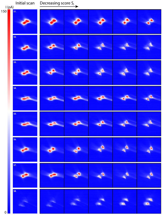
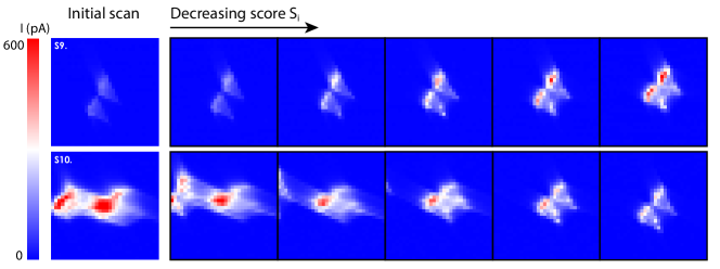
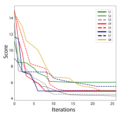
The optimisation of different pairs of bias triangles is shown in Fig. S2 (cases S1 to S8) and Fig. S3 (cases S9 and S10). The stability diagrams correspond to gate voltage configurations for which a decrease in score is observed. Fig. S4 presents the VAE score as a function of the number of iterations of the optimisation algorithm for the optimisation cases in Fig. S2 and Fig. S3. The total gate voltage changes during fine-tuning are presented in Table LABEL:table1.
| Case | |||||
|---|---|---|---|---|---|
| 1 | -8.0 | 0 | 6.29 | 5.92 | -6.0 |
| 2 | -6.0 | -8.0 | 6.57 | 0 | 6.0 |
| 3 | -4.0 | -8.0 | 5.26 | 1.97 | 0 |
| 4 | 6.0 | 4.0 | -3.94 | -7.89 | 10.0 |
| S1 | -10.0 | 0 | 5.26 | 4.60 | 0 |
| S2 | -4.0 | -10.0 | 5.92 | 1.31 | 0 |
| S3 | 0 | -8.0 | 2.63 | 0 | -2.0 |
| S4 | -6.0 | -2.0 | 3.94 | 1.97 | 2.0 |
| S5 | -4.0 | -6.0 | 4.60 | 0.66 | 2.0 |
| S6 | 0 | -8.0 | 3.29 | -1.31 | 2.0 |
| S7 | -2.0 | -8.0 | 3.94 | 0.66 | 0 |
| S8 | 14.0 | 0 | -7.23 | -9.86 | 4.0 |