Current detection using a Josephson parametric upconverter
Abstract
We present the design, measurement and analysis of a current sensor based on a process of Josephson parametric upconversion in a superconducting microwave cavity. Terminating a coplanar waveguide with a nanobridge constriction Josephson junction, we observe modulation sidebands from the cavity that enable highly sensitive, frequency-multiplexed output of small currents for applications such as transition-edge sensor array readout. We derive an analytical model to reproduce the measurements over a wide range of bias currents, detunings and input powers. Tuning the frequency of the cavity by more than with DC current, our device achieves a minimum current sensitivity of . Extrapolating the results of our analytical model, we predict an improved device based on our platform, capable of achieving sensitivities down to , or even lower if one could take advantage of parametric amplification in the Josephson cavity. Taking advantage of the Josephson architecture, our approach can provide higher sensitivity than kinetic inductance designs, and potentially enables detection of currents ultimately limited by quantum noise.
I Introduction
Ultra-low noise radiation detection has applications in astronomy, particle physics, and quantum information processing. In particular, transition edge sensors (TES) allow for broadband radiation detection with exceptionally low noise equivalent power Goldie et al. (2011) and photon number resolution Cabrera et al. (1998); Miller et al. (2003). To read out the small changes in current of TES in response to radiation absorption, highly sensitive current amplifiers such as superconducting quantum interference devices (SQUIDs) can be used with sensitivities as low as Gay et al. (2000). However, with the increasing number of TES to be read out simultaneously in multipixel detectors, SQUID amplifiers significantly increase system cost and complexity, especially when employing frequency-domain multiplexing to reduce the number of necessary amplifiers Henderson et al. (2016).
An example of recently developed current detectors as a replacement of SQUIDs are kinetic inductance parametric upconverters (KPUPs), also referred to as microwave kinetic inductance nanowire galvanometers, which rely on the changing kinetic inductance of a narrow superconducting wire embedded in a microwave circuit in response to a DC bias current, with state of the art devices reaching current sensitivities between Kher et al. (2016); Doerner et al. (2018); Kuzmin et al. (2018). One could potentially achieve a higher response from such a cavity detector by replacing the nanowire kinetic inductance element with a Josephson junction (JJ), enabling detection of currents using a Jospheson parametric upconverter (JPUP). This would also enable the incorporation of processes such as Josephson parametric amplification, which allows signals to be amplfied with quantum limited noise Stehlik et al. (2015), directly in the readout cavity.
Typically, the integration of JJs in superconducting microwave circuits is technologically more demanding due to the additionally needed fabrication steps to avoid aging effects and low coherence at microwave frequencies Pavolotsky et al. (2011); Goteti et al. (2019); Gunnarsson et al. (2013); Yanai and Steele (2019). The intrinsically large Kerr-nonlinearity of JJs Wallraff et al. (2004) can additionally place an upper limit on the device power allowed for circuit operation, which calls for either large critical current JJs with additional fabrication challenges Lecocq et al. (2011), or appropriate circuit design for sufficiently diluting the nonlinearity to provide stable device operation.
Here, we provide experimental realisation of a JPUP based on a hybrid combination of a direct current (DC) accessible microwave cavity in coplanar waveguide (CPW) geometry Bosman et al. (2015); Schmidt et al. (2018). The design uses a constriction JJ fabricated in the same step and layer as the microwave cavity which simplifies the fabrication procedure and allows for high cavity drive powers Vijay et al. (2009); Kennedy et al. (2019); Rodrigues et al. (2019); Bothner et al. (2019). We show device operation by converting current signals to the range, and reproduce the data with an analytical model for a wide range of bias currents, drive detunings and drive powers. Our device achieves performance comparable to KPUP technology, with the potential to provide enhanced current sensitivity with a more optimized design. Ultimately, by using Josephson parametric amplification in the same cavity as used for sensing, the JPUP could sense low frequency currents with a sensitivity limited by quantum noise.
II The DC bias microwave circuit
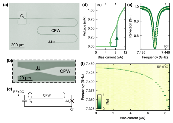
The device consists of a galvanically accessible microwave cavity, formed by a CPW that is shunted by an input capacitor and shorted to ground at its far end by a JJ, as depicted in Figs. 1(a-c). The JJ is formed by a narrow constriction in the superconducting base-layer, which allows us to fabricate it in the same step as the microwave circuit. For details on the fabrication procedure, see Sec. SII of the Supplemental Material See . Due to the shunt capacitor allowing low-frequency signals to pass through, but acting as a semi-transparent mirror for microwave frequencies, our circuit allows for simultaneous measurements in the DC and RF regimes.
In the DC regime, the CPW center conductor acts as a long lead to the JJ, which we use to perform a current-voltage measurement to characterize the JJ. Upon applying an increasing DC bias current, the JJ switches from the superconducting to the voltage state and back again at switching and retrapping currents and , as shown in Fig. 1(d). The observed hysteresis is most likely a combination of the capacitances of the CPW and shunt capacitor, and local heating in the junction area, cf. Refs. Tinkham (1996); Skocpol et al. (1974); Hazra et al. (2010); Kumar et al. (2015) and Sec. SIV in the Supplemental Material See .
In the RF regime, the JJ acts as a nonlinear inductor, with its inductance depending on the amount of bias current flowing through it, according to
| (1) |
with the critical current and the magnetic flux quantum. For zero bias current, both the impedance of shunt capacitor and of the JJ are small compared to the characteristic impedance of the CPW, i.e. . The CPW can thus host a fundamental half-wavelength () mode with current antinodes at both ends. When recording the reflected signal of the device using single-tone RF spectroscopy, the reflection signal shows a dip in the spectrum as seen in Fig. 1(e). We fit the data using the reflection coefficient of our circuit,
| (2) |
with the detuning between a drive at and the resonance frequency and the external and internal loss rates and , respectively. At zero bias current, we find a resonance frequency of , and linewidths of and .
As we DC-bias the circuit, increases, effectively shifting the voltage antinode closer to the JJ. This results in a continuously decreasing resonance frequency, tuning over approximately , cf. Fig. 1(f). We can approximate the bias current dependence of the cavity resonance frequency with a model describing a CPW resonator terminated by a JJ via
| (3) |
with the resonance frequency of the CPW directly shorted to ground and the total bare resonator inductance (see Sec. SIII.3 of the Supplemental Material See and Ref. Pogorzalek et al. (2017)). We use this model to fit the measured resonance frequencies in Fig. 2(a), from which we extract , and . The resonator inductance agrees with the value expected from our circuit design. The critical current as inferred from the microwave measurement is approximately larger than the DC switching current. We suspect that current noise in the DC line leads to premature switching of the JJ in the IV measurements, resulting in , as discussed in Sec. SV of the Supplemental Material See and Ref. Kautz and Martinis (1990). On the other hand, the RF measurement is sensitive to the Josephson inductance, from which we can infer the critical current in a less perturbative way. We note that current-biasing a superconducting wire will also change its kinetic inductance Annunziata et al. (2010); Vissers et al. (2015). However, while our device does possess a noticeable kinetic inductance fraction Gao et al. (2006), the changes in within the range of applied bias currents are negligible compared to and we thus attribute the resonance frequency shift completely to the latter, cf. Sec. SIII.2 of the Supplemental Material See .
III Current detection by frequency up-conversion
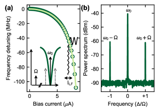
Figure 2(a) illustrates the principle of current detection using the DC biased Josephson cavity. To detect small modulation currents, we drive the cavity on resonance and simultaneously modulate the bias point with a low-frequency signal , so that the total current is given by . The responsivity of the resonance frequency to bias current,
| (4) |
exceeds for . As a consequence, once the resonance frequency is modulated by , phase modulation leads to the generation of sidebands in the microwave drive tone reflection with , where . The reflected cavity field thus exhibits the drive tone together with the sidebands, as depicted in Fig. 2(b).
The general equation of motion for the amplitude field of a harmonic high- oscillator with small nonlinearity , written in the frame rotating with the drive, is given by
| (5) |
with the amplitude of the drive field in units of at , and a small nonlinearity Castellanos-Beltran (2010). We consider the case in which the cavity resonance frequency is a function of an additional current given by , such that
| (6) | ||||
The resulting field amplitude of the first order sidebands appearing at is
| (7) |
In our experiment, we chose and . In this case, and red () and blue () sidebands have approximately equal amplitudes, see Sec. SVI of the Supplemental Material See . Note that even higher order contributions from the current still contribute to the sideband, but those contributions can be neglected for relatively weak modulation.
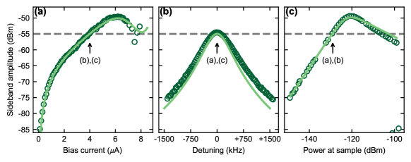
To explore the parameter space of our device, we performed a series of current-mixing measurements for different values of bias current , drive detuning and drive amplitude , for all of which we observe excellent agreement between experiment and theory: As can be seen in Fig. 3(a), for the case of varying bias current and as expected from Eqs. (3),(7), the first order sideband vanishes for zero bias current. As we increase the DC bias current, the increasing Josephson inductance leads to an increased responsivity , which in turn results in a growing sideband amplitude. Assuming all other parameters remain constant, the sideband amplitude should keep growing until the bias current reaches the critical current of the JJ, at which point the junction switches to the normal state, effectively destroying the device response. However, already at the sideband amplitude exhibits a maximum value and begins to decrease subsequently. The origin for this phenomenon lies in the growth of for increasing , which limits the maximum achievable sideband amplitude, cf. Sec.IV.2 and Sec. SV of the Supplemental Material See .
Operating the device at constant bias current and drive power but sweeping the drive tone with respect to the cavity resonance similarly reduces the sideband amplitude, which is reflected in both the theoretical model and our measurements, cf. Fig. 3(b). We attribute deviations of the model from the data to an effectively increased cavity linewidth resulting from a noise-induced fluctuating cavity frequency.
Finally, when setting the detuning back to zero and sweeping the drive power, we initially observe a linear increase of the sideband amplitude, cf. Fig. 3(c). This is in good agreement with the intracavity field dependence with pump power of a linear cavity. However, due to the nonlinearity of the JJ and the resulting Kerr anharmonicity of the circuit, our device enters the Duffing regime for large input powers, resulting in the observable reduction of the sideband amplitude: The anharmonicity results in a down shifted resonance frequency given by . In the measurement depicted in Fig. 3(c), the only varying parameter is the pump power, which means that in the Duffing regime the drive acquires an increase in detuning for increased power, resulting in a decreased sideband amplitude, as we saw earlier.
IV Current sensitivity
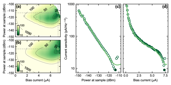
Having established the validity of our theoretical framework, we calculate the current sensitivity of our device. This quantity captures the minimum current that the device is able to discriminate from the noise floor. We obtain this quantity by extracting the signal-to-noise ratio (SNR) of the first sideband amplitude: Since we know the amplitude of our ingoing LF current signal, we can convert the sideband amplitude and noise floor to currents as described in Sec. SIX of the Supplemental Material See . We obtain
| (8) |
with ENBW the equivalent noise bandwidth of the spectrum analyzer Rauscher et al. (2016), and and the amplitudes of the sideband and the noisefloor in , respectively.
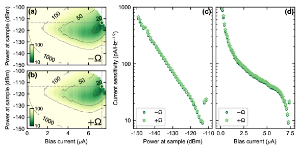
IV.1 Measured device
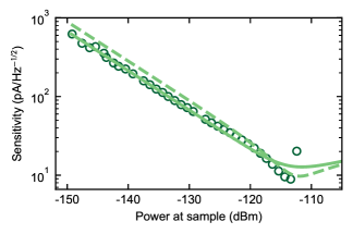
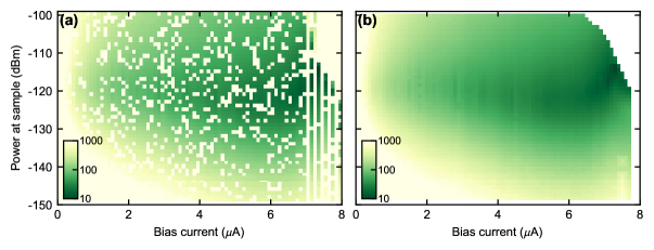
We analyze for a large range of bias currents and drive powers. The device sensitivities extracted via Eq. (8) are plotted in Figs. 4(a,b) for the measured and modeled data, respectively, showing good qualitative agreement. Linecuts through the 2D measured and simulated data at the best measured value of show good quantitative agreement between theoretical model and measurement, cf. Figs. 4(c,d). For a fixed bias current, the current sensitivity drops exponentially as a function of input power, reaching a minimum value of at and . Similarly, as a function of bias current and fixed input power, the current sensitivity drops rapidly over more than two orders of magnitude. Our theoretical calculations deviate from the measured data for very large input powers and bias currents, for which the model predicts sensitivity values larger than observed. This deviation might be due to minor differences in experimental and theoretical detuning: If the the pump tone is slightly below the value of in the limit of , the pump will initially be slightly red-detuned () and move to blue-detuned () as the resonance shifts downward due to the Kerr nonlinearity, instead of starting on-resonance and becoming only blue-detuned as we increase . Depending on the pump power at which , the theory curve will underestimate the sideband amplitude for , resulting in too large values of , as in Fig. 4(c) for . As detailed in Sec. SVIII of the Supplemental Material See , the model follows the measured data more closely for high pump powers assuming an initially red detuned drive. This deviation is especially large for high bias currents because the anharmonicity grows with . Thus, the cavity resonance shifts stronger with pump power and the drive is more likely to have a smaller detuning than expected for high .
IV.2 Limitations of present device and setup
Optimum sensitivity would be achieved for zero pump detuning, maximum pump power and biasing the device close to , cf. Fig.4(a),(b). In our experiment we were unable to operate the device in a stable regime for bias currents greater than , after which the JJ occasionally switched to the normal state, destroying the RF resonance. Additionally, we observed exponential increase of the internal loss rate for large bias currents. These effects are presumably due to random phase diffusion across the junction and electrical interference in our setup, cf. Sec. SV of the Supplemental Material See . Most notably, at elevated bias currents spurious sidebands at integer multiples of appear in the measured spectra, which are due to insufficient isolation between the DC and RF electronics. Using the same approach as for the intended signal, we can quantify the current noise due to mains power to . Improving the setup should allow us to move to even higher bias currents, gaining in . In addition, the resonance frequency shift due to anharmonicity places an upper bound on the maximum input power. In an optimized measurement, shifting the pump frequency with pump power in order to remain closer to resonance should allow us to gain more than , reaching a minimum of , cf. Sec SVII of the Supplemental Material See .
IV.3 Modeled optimized device
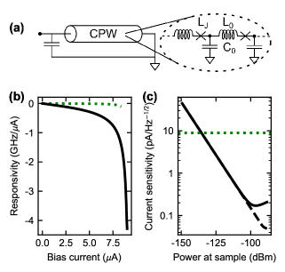
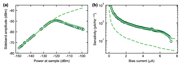
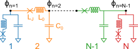
In order to improve , we propose a slightly changed circuit layout that follows naturally from the measured device and is immediately implementable: Instead of a transmission line shorted to ground by a single JJ, we propose to incorporate the Josephson inductance into the transmission line itself, by means of a diluted JJ metamaterial Planat et al. (2019). The optimized design would then be a transmission line directly shorted to ground, with the CPW center conductor made up of a series of identical unit cells, each composed of a combination of linear and Josephson inductance () and a capacitance to ground (), as depicted in Fig. 5(a). Following the approach to circuit quantization presented in Ref. Gely and Steele (2019) and methods from Refs. Noschese et al. (2013); Nigg et al. (2012); Vool and Devoret (2017), we derive the resonance frequency of this CPW as
| (9) |
in the limit of large , as detailed in Sec.SXI of the Supplemental Material See . To maximize the responsivity of the device via maximizing the participation ratio per unit cell, we propose a CPW with center conductor and gap sizes of the current design and a reasonably short unit cell length of . This would result in , and per unit cell, cf. Ref. Simons (2001) and Sec. SXI of the Supplemental Material See . For an initial resonance frequency at , the device would require approximately 845 unit cells, resulting in a total device length of , much more compact than our present layout. Such an optimized device offers a significantly larger with a relative frequency shift . Additionally increasing the external coupling, e.g. by reducing the shunt capacitor to of its current size, this device would be able to achieve sensitivities as low as , a factor of 54 improvement to our presented design, as shown in Fig. 5(b). We note that in an ideal experiment, the drive frequency should be tuned for increasing drive power in order to account for the Kerr-shift of the resonance to lower frequencies, thus minimizing and maximizing . Implementing this measurement scheme would allow us to achieve sensitivities down to . Since this estimation does not take parametric amplification into account, we expect it to be an upper bound to the experimentally achievable : Utilizing quantum-limited parametric amplification built into the device would allow us to gain approximately Stehlik et al. (2015); Pogorzalek et al. (2017); Planat et al. (2019), providing noise levels down to .
V Conclusion
We presented a Josephson parametric upconverter and demonstrated current sensitivities down to which makes our compatible with TES readout, and derived an analytical model that accurately reproduces the measured data and is immediately applicable to other device architectures. We estimate that future devices using increased Josephson participation ratios, and using the intrinsic Kerr-nonlinearity for four-wave parametric amplification built into the detection cavity, should allow for an increase , orders of magnitude better than state of the art KPUPs and limited by the fundamental quantum noise of the cavity.
Data availability
All raw and processed data as well as supporting code for measurement libraries, data processing and figure generation is available in Zenodo Schmidt et al.
Acknowledgements
This project has received funding from the European Union Horizon 2020 research and innovation programme under grant agreement Nos. 681476 – QOMD, 732894 – HOT and 785219 – GrapheneCore2.
Appendix A Input-output formalism
Starting from Eq. (5), with the steady-state solution , the reflection coefficient is given by
| (10) |
where the second equality holds in the limit and which can be recognized as the usual reflection expression of circuit theory.
We now consider the case in which the cavity resonance frequency is a function of an additional current given by . With the resonance frequency given by Eq. (6), the new equation of motion reads
| (11) | ||||
With the Ansatz for the intracavity field and assuming we get
| (12) | ||||
Let the modulation in current be of the form
| (13) |
where . Our Ansatz for is consequently
| (14) |
Inserting Eqs. (13),(14) into Eq. (12), we can group the terms by their frequency components and equalize each component individually in order to solve for the sideband coefficients . Each sideband output field can then be calculated via
| (15) |
We arrive at a compact result for the first order sidebands appearing at :
| (16) |
We calculated all coefficients up to using Mathematica v11.3.0.0 in the notebook input-output formalism.nb, which we subsequently converted to python3 code using the notebook Export to Python.nb located in Zenodo Schmidt et al. .
Appendix B Calculating the steady-state solution
We can calculate by solving Eq. (5) for a large pump signal and treating the probe as a perturbation Castellanos-Beltran (2010). Thus, let us assume that the solution has the form and the input signal is the pump signal. Since we are only interested in the steady-state solution, let . Inserting this into Eq. (5), we get
| (17) |
Multiplying this equation with its complex conjugate returns
| (18) |
While this third-order polynomial in has multiple complex solutions, the ones relevant in our case are only real. In the high-power regime, our resonator will exhibit bifurcation and Duffing behavior, meaning there will be three real valued solutions to : The largest, median and smallest one corresponding to the high, middle and low amplitude branch, respectively. For a given input field and detuning , the (up to three) solutions of this equation can be found either numerically or analytically. However, for the parameters used in our experiment, the solutions for are identical because our drive remains outside of the bifurcation regime. We can then use the corrected intracavity field for obtaining the sideband amplitudes by replacing the value of for the linear oscillator in Eq. (S8).
Furthermore, taking the resonance frequency as the point where , we can compute the frequency shift the cavity experiences as a result of the driving power by differentiating Eq. (18) with respect to as
| (19) |
Appendix C Higher order terms
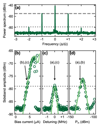
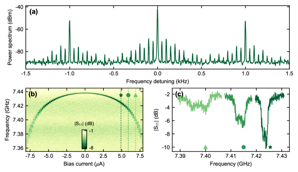
Already for second order in , the prefactors are too complicated to write down in a short form, which is why we refer to the full analytical solutions in the Mathematica notebook input-output formalism.nb located on Zenodo Schmidt et al. . We note that higher order corrections arising for terms in , have only negligible effects on the lower order forms. For the analysis in the main text, we therefore only make use of the closed form for the first order terms, and for the second order peaks in Fig. 6(b-d), only the second order terms were used.
We observe higher order sidebands over a wide range of operating points, with an exemplary spectrum exhibiting both first and second order peaks plotted in Fig. 6(a). Similar to Fig. 3(a), the second order sideband increases with DC bias current up to where the amplitude is limited by the increasing internal loss rate, cf. Fig. 6(b). As depicted in Fig. 6(c), finite drive detuning strongly suppresses the sideband amplitude similar to the first order peaks. The power dependence, cf. Fig. 6(c), also closely resembles the shape of the first order sideband, with maximum amplitude for high drive powers and subsequent decrease due to increasing drive detuning as a consequence of the downshift in resonance frequency due to the Kerr nonlinearity.
References
- Goldie et al. (2011) D. J. Goldie, A. V. Velichko, D. M. Glowacka, and S. Withington, “Ultra-low-noise MoCu transition edge sensors for space applications,” Journal of Applied Physics 109, 084507 (2011).
- Cabrera et al. (1998) B. Cabrera, R. M. Clarke, P. Colling, A. J. Miller, S. Nam, and R. W. Romani, “Detection of single infrared, optical, and ultraviolet photons using superconducting transition edge sensors,” Applied Physics Letters 73, 735–737 (1998).
- Miller et al. (2003) A. J. Miller, S. W. Nam, J. M. Martinis, and A. V. Sergienko, “Demonstration of a low-noise near-infrared photon counter with multiphoton discrimination,” Applied Physics Letters 83, 791–793 (2003).
- Gay et al. (2000) F. Gay, F. Piquemal, and G. Genevès, “Ultralow noise current amplifier based on a cryogenic current comparator,” Review of Scientific Instruments 71, 4592–4595 (2000).
- Henderson et al. (2016) S. W. Henderson, J. R. Stevens, M. Amiri, J. Austermann, J. A. Beall, S. Chaudhuri, H.-M. Cho, S. K. Choi, N. F. Cothard, K. T. Crowley, S. M. Duff, C. P. Fitzgerald, P. A. Gallardo, M. Halpern, M. Hasselfield, G. Hilton, S.-P. P. Ho, J. Hubmayr, K. D. Irwin, B. J. Koopman, D. Li, Y. Li, J. McMahon, F. Nati, M. Niemack, C. D. Reintsema, M. Salatino, A. Schillaci, B. L. Schmitt, S. M. Simon, S. T. Staggs, E. M. Vavagiakis, and J. T. Ward, “Readout of two-kilopixel transition-edge sensor arrays for Advanced ACTPol,” in SPIE Astronomical Telescopes + Instrumentation, edited by W. S. Holland and J. Zmuidzinas (Edinburgh, United Kingdom, 2016) p. 99141G.
- Kher et al. (2016) A. Kher, P. K. Day, B. H. Eom, J. Zmuidzinas, and H. G. Leduc, “Kinetic Inductance Parametric Up-Converter,” Journal of Low Temperature Physics 184, 480–485 (2016).
- Doerner et al. (2018) S. Doerner, A. Kuzmin, K. Graf, I. Charaev, S. Wuensch, and M. Siegel, “Compact microwave kinetic inductance nanowire galvanometer for cryogenic detectors at 4.2 K,” Journal of Physics Communications 2, 025016 (2018).
- Kuzmin et al. (2018) A. Kuzmin, S. Doerner, S. Singer, I. Charaev, K. Ilin, S. Wuensch, and M. Siegel, “Terahertz Transition-Edge Sensor With Kinetic-Inductance Amplifier at 4.2 K,” IEEE Transactions on Terahertz Science and Technology 8, 622–629 (2018).
- Stehlik et al. (2015) J. Stehlik, Y.-Y. Liu, C. M. Quintana, C. Eichler, T. R. Hartke, and J. R. Petta, “Fast Charge Sensing of a Cavity-Coupled Double Quantum Dot Using a Josephson Parametric Amplifier,” Physical Review Applied 4, 014018 (2015).
- Pavolotsky et al. (2011) A. B. Pavolotsky, D. Dochev, and V. Belitsky, “Aging- and annealing-induced variations in Nb/Al–AlOx/Nb tunnel junction properties,” Journal of Applied Physics 109, 024502 (2011).
- Goteti et al. (2019) U. S. Goteti, M. Denton, K. Krause, A. Stephen, J. A. Sellers, S. Sullivan, M. C. Hamilton, A. Wynn, and S. K. Tolpygo, “Reliability Studies of Nb/AlOx/Al/Nb Josephson Junctions Through Accelerated-Life Electrical Stress Testing,” IEEE Transactions on Applied Superconductivity 29, 1–7 (2019).
- Gunnarsson et al. (2013) D. Gunnarsson, J.-M. Pirkkalainen, J. Li, G. S. Paraoanu, P. Hakonen, M. Sillanpää, and M. Prunnila, “Dielectric losses in multi-layer Josephson junction qubits,” Superconductor Science and Technology 26, 085010 (2013).
- Yanai and Steele (2019) S. Yanai and G. A. Steele, “Observation of enhanced coherence in Josephson SQUID cavities using a hybrid fabrication approach,” arXiv:1911.07119 [cond-mat] (2019), arXiv:1911.07119 [cond-mat] .
- Wallraff et al. (2004) A. Wallraff, D. I. Schuster, A. Blais, L. Frunzio, R.-S. Huang, J. Majer, S. Kumar, S. M. Girvin, and R. J. Schoelkopf, “Strong coupling of a single photon to a superconducting qubit using circuit quantum electrodynamics,” Nature 431, 162–167 (2004).
- Lecocq et al. (2011) F. Lecocq, I. M. Pop, Z. Peng, I. Matei, T. Crozes, T. Fournier, C. Naud, W. Guichard, and O. Buisson, “Junction fabrication by shadow evaporation without a suspended bridge,” Nanotechnology 22, 315302 (2011).
- Bosman et al. (2015) S. J. Bosman, V. Singh, A. Bruno, and G. A. Steele, “Broadband architecture for galvanically accessible superconducting microwave resonators,” Applied Physics Letters 107, 192602 (2015).
- Schmidt et al. (2018) F. E. Schmidt, M. D. Jenkins, K. Watanabe, T. Taniguchi, and G. A. Steele, “A ballistic graphene superconducting microwave circuit,” Nature Communications 9, 4069 (2018).
- Vijay et al. (2009) R. Vijay, J. D. Sau, M. L. Cohen, and I. Siddiqi, “Optimizing Anharmonicity in Nanoscale Weak Link Josephson Junction Oscillators,” Physical Review Letters 103, 087003 (2009).
- Kennedy et al. (2019) O. Kennedy, J. Burnett, J. Fenton, N. Constantino, P. Warburton, J. Morton, and E. Dupont-Ferrier, “Tunable Nb Superconducting Resonator Based on a Constriction Nano-SQUID Fabricated with a Ne Focused Ion Beam,” Physical Review Applied 11, 014006 (2019).
- Rodrigues et al. (2019) I. C. Rodrigues, D. Bothner, and G. A. Steele, “Coupling microwave photons to a mechanical resonator using quantum interference,” Nature Communications 10, 5359 (2019).
- Bothner et al. (2019) D. Bothner, I. C. Rodrigues, and G. A. Steele, “Photon-Pressure Strong-Coupling between two Superconducting Circuits,” arXiv:1911.01262 [cond-mat, physics:quant-ph] (2019), arXiv:1911.01262 [cond-mat, physics:quant-ph] .
- (22) “See Supplemental Material at [URL will be inserted by publisher] for details on device fabrication, device parameters, hysteresis of switching currents, measurement setup, data processing and mathematical derivations.” .
- Tinkham (1996) M. Tinkham, Introduction to Superconductivity, 2nd ed. (McGraw-Hill, Inc., New York, 1996).
- Skocpol et al. (1974) W. J. Skocpol, M. R. Beasley, and M. Tinkham, “Self-heating hotspots in superconducting thin-film microbridges,” Journal of Applied Physics 45, 4054–4066 (1974).
- Hazra et al. (2010) D. Hazra, L. M. A. Pascal, H. Courtois, and A. K. Gupta, “Hysteresis in superconducting short weak links and -SQUIDs,” Physical Review B 82, 184530 (2010).
- Kumar et al. (2015) N. Kumar, T. Fournier, H. Courtois, C. B. Winkelmann, and A. K. Gupta, “Reversibility Of Superconducting Nb Weak Links Driven By The Proximity Effect In A Quantum Interference Device,” Physical Review Letters 114, 157003 (2015).
- Pogorzalek et al. (2017) S. Pogorzalek, K. G. Fedorov, L. Zhong, J. Goetz, F. Wulschner, M. Fischer, P. Eder, E. Xie, K. Inomata, T. Yamamoto, Y. Nakamura, A. Marx, F. Deppe, and R. Gross, “Hysteretic Flux Response and Nondegenerate Gain of Flux-Driven Josephson Parametric Amplifiers,” Physical Review Applied 8, 024012 (2017).
- Kautz and Martinis (1990) R. L. Kautz and J. M. Martinis, “Noise-affected I-V curves in small hysteretic Josephson junctions,” Physical Review B 42, 9903–9937 (1990).
- Annunziata et al. (2010) A. J. Annunziata, D. F. Santavicca, L. Frunzio, G. Catelani, M. J. Rooks, A. Frydman, and D. E. Prober, “Tunable superconducting nanoinductors,” Nanotechnology 21, 445202 (2010).
- Vissers et al. (2015) M. R. Vissers, J. Hubmayr, M. Sandberg, S. Chaudhuri, C. Bockstiegel, and J. Gao, “Frequency-tunable superconducting resonators via nonlinear kinetic inductance,” Applied Physics Letters 107, 062601 (2015).
- Gao et al. (2006) J. Gao, J. Zmuidzinas, B. A. Mazin, P. K. Day, and H. G. Leduc, “Experimental study of the kinetic inductance fraction of superconducting coplanar waveguide,” Nuclear Instruments and Methods in Physics Research Section A: Accelerators, Spectrometers, Detectors and Associated Equipment Proceedings of the 11th International Workshop on Low Temperature Detectors, 559, 585–587 (2006).
- Castellanos-Beltran (2010) M. A. Castellanos-Beltran, Development of a Josephson Parametric Amplifier for the Preparation and Detection of Nonclassical States of Microwave Fields, Ph.D. thesis, University of Colorado, Boulder (2010).
- Rauscher et al. (2016) C. Rauscher, V. Janssen, and R. Minihold, Fundamentals of Spectrum Analysis, 9th ed. (Rohde & Schwarz, München, 2016) oCLC: 964521293.
- Planat et al. (2019) L. Planat, R. Dassonneville, J. P. Martínez, F. Foroughi, O. Buisson, W. Hasch-Guichard, C. Naud, R. Vijay, K. Murch, and N. Roch, “Understanding the Saturation Power of Josephson Parametric Amplifiers Made from SQUID Arrays,” Physical Review Applied 11, 034014 (2019).
- Gely and Steele (2019) M. F. Gely and G. Steele, “QuCAT: Quantum Circuit Analyzer Tool in Python,” New Journal of Physics (2019), 10.1088/1367-2630/ab60f6.
- Noschese et al. (2013) S. Noschese, L. Pasquini, and L. Reichel, “Tridiagonal Toeplitz matrices: Properties and novel applications,” Numerical Linear Algebra with Applications 20, 302–326 (2013).
- Nigg et al. (2012) S. E. Nigg, H. Paik, B. Vlastakis, G. Kirchmair, S. Shankar, L. Frunzio, M. H. Devoret, R. J. Schoelkopf, and S. M. Girvin, “Black-Box Superconducting Circuit Quantization,” Physical Review Letters 108, 240502 (2012).
- Vool and Devoret (2017) U. Vool and M. Devoret, “Introduction to quantum electromagnetic circuits: Introduction to quantum electromagnetic circuits,” International Journal of Circuit Theory and Applications (2017), 10.1002/cta.2359.
- Simons (2001) R. N. Simons, Coplanar Waveguide Circuits, Components, and Systems, edited by K. Chang, Wiley Series in Microwave and Optical Engineering (John Wiley & Sons, Inc., New York, USA, 2001).
- (40) F. E. Schmidt, D. Bothner, I. C. Rodrigues, M. F. Gely, M. D. Jenkins, and G. A. Steele, “Data and processing for “Current detection using a Josephson parametric upconverter”,” DOI.
Supplementary Material:
Current detection using a Josephson parametric upconverter
Felix E. Schmidt, Daniel Bothner, Ines C. Rodrigues, Mario F. Gely, Mark D. Jenkins, and Gary A. Steele∗
Kavli Institute of NanoScience, Delft University of Technology, Lorentzweg 1, 2628 CJ, Delft, The Netherlands.
Appendix SI Measurement setup
SI.1 Wiring configuration
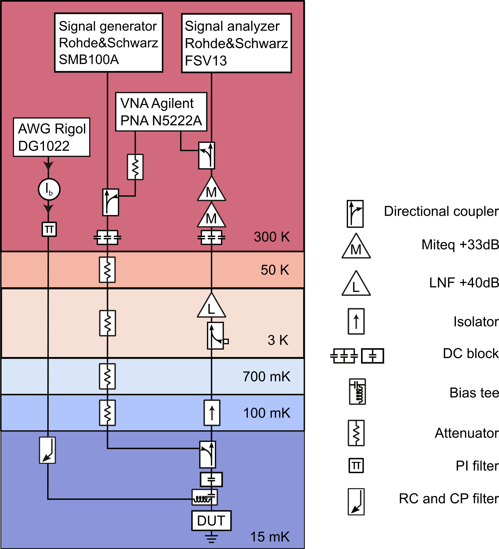
All measurements were taken with the device mounted to the millikelvin stage of a Bluefors BF 400-D dilution refrigerator with a base temperature of approximately . The measurement setup is sketched in Fig. S1. We use in-house built, low-noise battery powered electronics for DC biasing of the device. For measurements involving current detection, we modulate the voltage controlled current source with an arbitrary waveform generator (AWG), model DG1022Z from Rigol. Microwave reflection measurements of the cavity are done using a vector network analyzer (VNA) from Agilent, model PNA N5222A. Signal generation and spectroscopy for current detection are done using signal generator SMB 100A (SG) and analyzer FSV13 (SA), respectively, from Rohde & Schwarz. The VNA and SG paths are merged using directional couplers. Prior to the measurements on current detection, we calibrated the frequency dependent difference in attenuation between the signal paths VNA – device under test (DUT) and SG – DUT which we account for in all measurements and in the data analysis.
In order to minimize the influence of interference from mains powered equipment on our experiments, we place the DC electronics on an isolated rack and place all RF equipment on another one. We observed significant signal deterioration for elevated bias currents if the DC and RF electronics shared the same ground. For this reason, we placed additional DC blocks with separated inner and outer conductors on the RF input lines (PE8212 from Pasternack). Note that for the LF current modulation, we need to galvanically connect the AWG to our battery-powered voltage controlled current source, which in turn leads to a potential source of significant interference (see Sec. SV for more elaborate discussion on this topic).
The DC lines are heavily filtered using -filters inside the room-temperature electronics, and homemade copper powder and two-stage RC-filters on the baseplate of the dilution refridgerator. The cut-off for these filters is at around , well above the chosen modulation frequency of .
SI.2 Measurement protocol for current detection
The measurements on current detection were performed using the following measurement scheme:
- 1. Initialization and calibration
-
Turn off all outputs of RF instruments. Sweep the bias current back to zero and then to the next bias value. Set the VNA output power to low power and perform an measurement from to . From this measurement, determine the resonance frequency as the frequency at which is minimum.
- 2. Current detection for fix pump power and detuning
-
Turn off the output of the VNA. Set the RF drive from the SG to low power and the drive frequency to . Turn on the LF modulation (, ). Trigger the SAto perform one measurement.
- 3. Current detection for variable detuning
-
Keep the RF pump power at the same value and sweep the RF modulation frequency from to and for each detuning record the output signal using the SA.
- 4. Current detection for variable pump power
-
Set the RF frequency back to . Sweep the RF pump power and for each pump power record the output signal using the SA. After each pump power measurement, reinitialize the bias current and find the resonance frequency again in order to reduce the number of ”dead” cases in which the Josephson junction switched to the voltage state prematurely.
SI.3 Estimation of the attenuation and amplification chain
To estimate the attenuation chain, we use the thermal noise of our cryogenic high electron mobility transistor (HEMT) as a calibration source. The noise power due to the effective noise temperature of the HEMT as given by the manufacturer is
| (S1) |
where is the measurement bandwidth of our setup. By averaging over a few traces taken with the VNA in an area unaffected by our DUT, i.e. off-resonant to the cavity and thus leaving the background unaltered in power, we extract an average signal and standard deviation which we use to define the signal-to-noise ratio at the VNA, for a VNA output power of .
In our setup, the added noise from the HEMT dominates over other noise sources, which we deduce from an increase in noise level when powering up the HEMT with the room temperature amplifiers already on. Therefore, the SNR at the VNA is identical to the one at the HEMT output, and we deduce the power arriving at the HEMT input to be . Between DUT and HEMT, the signal travels a certain distance of cabling and passes through additional microwave components, cf. Fig. S1. On the way, the signal will have been reduced by due to the mentioned components, hence the power arriving at the HEMT will be , which results in an estimated attenuation of of our VNA input line, assuming of cable loss between sample and HEMT.
We deduce the total gain of our amplification chain by calculating the average noise power measured with the SA, in a bandwidth, and substracting from it the HEMT noise power corresponding to the same bandwidth and the cable loss , resulting in a total gain of for the amplifier chain.
Appendix SII Device fabrication
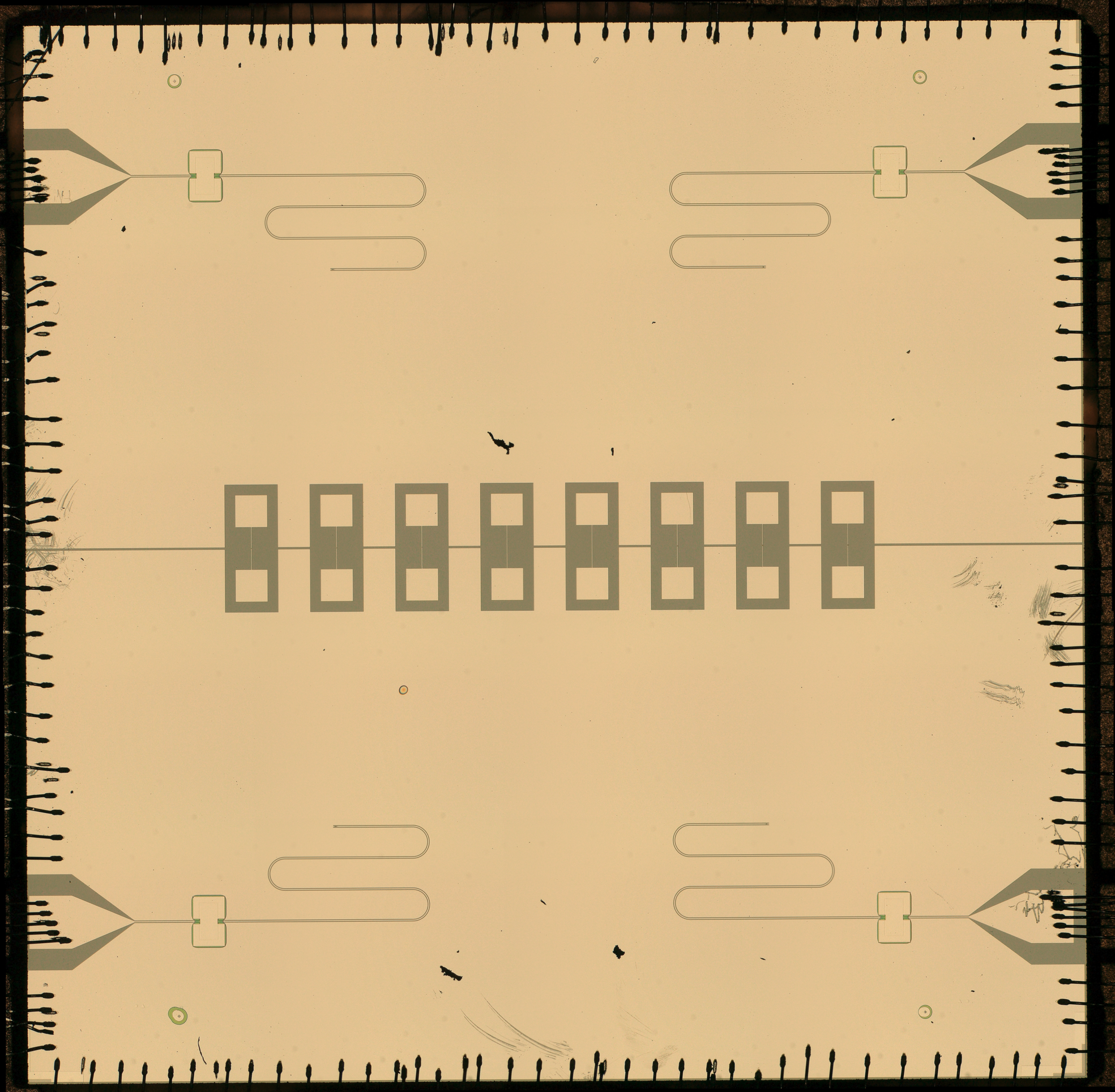
The device is fabricated in a four-step process in the Kavli Nanolab cleanroom of TU Delft, using a combination of electron beam lithography (EBL, EBPG5000+ from Raith), liftoff, sputtering (AC450 from Alliance), PECVD (PlasmaPro 80 from Oxford Instruments) and dry-etching (Fluorine reactive ion etcher from Leybold Hereaus). An optical micrograph of the fully packaged chip is shown in Fig. S2. The geometric device parameters are given in Table SI. In the following we describe the fabrication step by step.
- Substrate
-
We use a double-side polished high-resistivity (, light P/Boron doping, thickness) silicon wafer from IWS as substrate for our device. The wafer is covered in positive electron beam resist (AR-P 6200.13, approximate thickness ) and exposed to define the pattern for alignment and dicing markers. We sputter-deposit of Molybdenum-Rhenium (MoRe, RF magnetron sputtering in argon atmosphere from a Mo- Re target) and lift off the resist-protected areas using an anisole bath and strong ultrasonication, followed by multiple acetone and isopropanol baths. We subsequently cover the wafer with photoresist (HPR 504, thick) and dice it into chips for easier handling during fabrication.
- Base layer
-
We pattern the Josephson junction together with the base layer and ground planes in a single lift-off step using AR-P 6200.09 () and of sputtered Aluminum-Silicon (AlSi, reactive DC magnetron sputtering in argon atmosphere from a Al- Si target). Lift-off is done by placing the chip in the bottom of a beaker with room-temperature anisole and strong ultrasonication for a few minutes.
- Dielectric layer
-
For the shunt dielectric layer, we deposit amorphous silicon at using PECVD. Patterning is done with EBL of a double-layer resist (PMMA 950K A4 and AR-N 7700.18) and reactive ion etching in a \ceSF6 + He atmosphere. The resist layers are in-situ removed using \ceO2 plasma.
- Top shunt plate
-
The top plate of the shunt capacitor is fabricated with an additional lift-off step using the same resist as for the alignment markers, and sputtering \ceAlSi.
- Packaging
-
To fit our printed circuit board (PCB), the chip is again covered in photoresist and trimmed down to . After washing off the photoresist in a series of acetone and isopropanole baths, the chip is glued to our copper sample holder, to which the PCB is mounted, using cryogenic GE varnish. Electrical connections to the device are made using wedge-bonding on a Westbond wirebonder with aluminum wire bonds. We place a small copper lid on the chip to protect it from dirt and to suppress box modes of a bigger copper lid screwed onto the copper base, which accomodates the SMA connectors.
| Symbol | Description | Value |
|---|---|---|
| CPW center conductor | ||
| CPW gaps to ground | ||
| Base layer thickness | ||
| Geometric inductance per length Simons (2001) | ||
| Geometric capacitance per length Simons (2001) | ||
| CPW length, from end of shunt to JJ | ||
| Shunt capacitor area | ||
| Dielectric layer thickness |
Appendix SIII General device parameters
SIII.1 Reflection coefficient
The reflection coefficient of a transmission line with a shunt capacitor to ground on the input side and shorted to ground on the far end is given by
| (S2) |
with the detuning from resonance, and the internal, external and total loss rates , and .
The real response function is however distorted by the complex microwave background which arises due to impedance mismatches in our measurement setup. For this reason, we model the measured spectra using the above model for an ideal device multiplied by a complex microwave background and a rotation in the complex plane:
| (S3) |
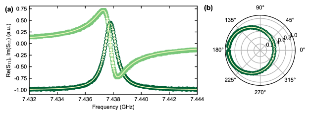
Our fitting algorithm first detects the resonance as frequency corresponding to the maximum phase derivative and fits the background signal by removing a certain window around the resonance frequency. In a second step, it fits the modified model to the full data set keeping the background parameters fixed, and finally refits all background and model parameters once more starting from the previously fitted values. A result of this fitting procedure, with background removed, is shown in Fig. S3.
SIII.2 Kinetic inductance estimation
Our AlSi films have a significant kinetic inductance contribution due to their small thickness of only . We estimate the kinetic inductance fraction by performing a finite element electromagnetic simulation using Sonnet v16.56 (Sonnet Software Inc., 2018) of the reference device (shorted to ground on the same chip, thus excluding the Josephson inductance) which results in an expected resonance due to only geometry at . We compare this value with the measured value of . The kinetic inductance fraction is given by Gao et al. (2006)
| (S4) |
which has a value of in our device, hence . Kinetic inductance also increases as a function of DC bias current via with the characteristic current Annunziata et al. (2010). The resulting downshift of the resonance frequency can be described by
| (S5) |
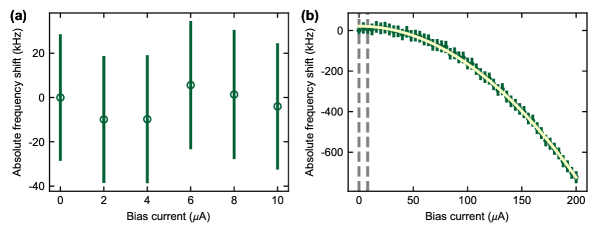
We emphasize however that in the JJ device, the sheet kinetic inductance is not the relevant tuning parameter: Biasing the reference device up to does not show a trend; instead the fluctuations in remain within the fitting errors, cf. Fig. S4(a). Only when applying bias currents up to , well beyond the values used for the measurements presented in the main text, does the resonance frequency of the reference device shift to lower frequencies, as shown in Fig. S4(b). We fit the data using Eq. (S5), extracting . This supports our claim that we can exclude kinetic inductance as an additional source of tuning the resonance frequency via applied bias currents and instead identify the Josephson inductance as the relevant tuning parameter.
SIII.3 Resonance frequency versus current due to Josephson inductance
Adapting the calculation for a Josephson terminated transmission line cavity given in Ref. Pogorzalek et al. (2017) to our device, we find for the current dependence of the cavity resonance frequency
| (S6) |
with the total device inductance, the resonance frequency without the JJ and the Josephson inductance given in Eq. (1) of the main text. We use this model to fit the measured resonance frequencies and extract , and . From the device geometry and kinetic inductance estimation, we expect , which is in acceptable agreement with the fit value.
Appendix SIV On the hysteresis of switching currents in our DC measurements
Accodring to a simple RCSJ model, hysteresis in Josephson junctions should occur only for JJ quality factors , with the junction capacitance Tinkham (1996). We perform finite element simulations with Sonnet v16.56 (Sonnet Software Inc., 2018) to estimate the stray capacitance of the metal leads in direct vicinity of the JJ (two pads separated by ) to be . Together with and , the junction would have . For , the ratio between retrapping and critical current can be approximated as . Hence, in order to satisfy our measured values, , which would be reached for . Likely, the geometric capacitance of the CPW and the surrounding ground planes significantly contributes and dominates the circuit capacitance: Already including a portion of the CPW increases to , satisfying this requirement. Additionally, we note that local heating in the junction area can also play a significant role, reducing further Skocpol et al. (1974); Hazra et al. (2010); Kumar et al. (2015).
Appendix SV On the increased loss rates for increased bias current
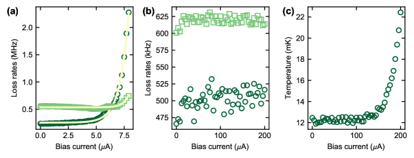
We observed an increase in the internal and external loss rates of the JJ terminated device for increased bias current, as can be seen in Fig. S5(a). We can fit the loss rates quite accurately with a phenomenological exponential model of the form
| (S7) |
The extracted parameters for the device presented in the main text are given in Tab. SII. While should not directly depend on bias current, we do observe a slight increase, possibly due to changes in the impedance, linewidth broadening due to the increased or shifting the cavity through cable resonances. Regarding the increase in internal loss rate, we identified the following mechanisms as most likely:
- Electrical interference
-
While we physically disconnect all mains-powered equipment from our battery powered DC electronics, and placed DC blocks for both inner and outer conductors on the RF inputs to the fridge, we still notice a significant amount of interference on the measured spectra for high bias currents, cf. Fig. S6(a). We calculate the magnitude of the spurious signals to be approximately , or of . We assume that this interference is always present but only has noticeable effects for large . Since our RF spectroscopy measurement takes more than , the measured linewidth is effectively broadened by the moving cavity, induced by small-scale modulations. Note that the situation is significantly worse for an unoptimized setup (noise coupling into the DC electronics via ground): In this case, the cavity spectrum is extremely broadened and starts to resemble two dips for high , severely limiting the tuning range (c.f. Fig. S6(b) without, and Fig. 1(f) of the main text with isolation of the battery electronics from mains powered equipment). We estimate the interfering current signal for this case to be , significantly limiting any device operation in either DC or RF. The measurement setup could be further improved by choosing a LF modulation frequency which is not a higher order multiple of , such as , instead of . We note that there might be other frequencies at which interfering signals couple into our device. Electrical noise only cannot explain the observed increased loss rates because the latter are not simply proportional to .
- Phase diffusion
-
The shorted reference device exhibits constant and upon DC bias up to , at which point the mixing chamber starts to heat as we surpass the cooling power of for the LD400 Bluefors since the power dissipated in our low-pass filters reaches up to . In contrast, the temperature did not increase when measuring the JJ device. We therefore rule out quasiparticles (due to radiation or thermal excitations, Tinkham (1996))in the CPW as a significantly contributing loss mechanism. Instead, phase diffusion across the JJ can indeed play a significant role as the bias current approaches . Applying a DC current bias tilts the Josephson energy potential, enhancing the chance of phase-slip and quantum tunneling events, which can lead to dissipation even without switching to the normal state, as long as the phase particle is able to settle in the next washboard-potential minimum kiviojaWeakCouplingJosephson2005.
| Loss channel | () | () | () |
|---|---|---|---|
| Internal | |||
| External |
Appendix SVI Difference between first order red and blue sidebands
As derived in the main text, to first order in , the coefficients describing the sideband amplitudes are
| (S8) |
Without changing the device, our peak height will increase if we modulate the current stronger () or slower (), and by pumping harder (). With the same setup, increasing the current responsivity () would likewise enhance the peak height. Moreover, for small LF modulations , the peaks for red and blue sidebands should be equal in amplitude. In fact, the absolute difference between the two sidebands scales with
| (S9) |
for . Our experiments with support this statement, as we did not observe systematic differences between red and blue sidebands (cf Fig. S7) over the entire parameter space.
Appendix SVII Driving the cavity on resonance for high powers
To counteract acquired detuning from the downshift in resonance frequency for high pump powers due to the device nonlinearity, in an ideal measurement configuration the drive tone would also be shifted correspondingly. As depicted in Fig. S8, in such a situation, the sideband amplitude would keep increasing by more than , resulting in a minimum .
Appendix SVIII Deviations between data and theory for high powers
We observe deviations between the measured and modelled current sensitivity at high drive powers. As stated in the main text, assuming an initially red-detuned drive, i.e. in the limit of could explain this behavior. In Figure S9, we plot the data with the original model, and add an initial detuning of to the drive tune. While in this case the sensitivity is overestimated for small drive powers, the model follows the measured data closer for high powers than the calculations for zero initial detuning.
Appendix SIX Calculating the current sensitivity
The current sensitivity is defined by
| (S10) |
with the magnitude of the current noise and ENBW the equivalent noise bandwidth of the spectrum analyzer. In our experiment, the DUT converts the current modulation into an up-converted voltage signal, which we detect as the amplitude of the sidebands as in , with the signal height in . Additionally, we record the noise floor amplitude which sets the minimum detectable power, and the signal to noise ratio . Since the detected power is proportional to the square of the voltage field, which in turn is proportional to the input current, , we can infer the equivalent white current noise level of the HEMT and the sensitivity via
| (S11) | ||||
| (S12) |
For a Gaussian filter such as the one used in our setup, , with RBW the resolution bandwidth of the spectrum analyzer which was set to for all measurements Rauscher et al. (2016). In practice, we extract the sideband amplitude from the measured spectra as the peak power value at the expected and compute the noise floor as the average of the remaining data points.
Appendix SX Data visualization
Our raw measurements include a significant number of outliers in current sensitivity, visible as bright spots and streaks in Fig. S10(a). These are due to absent sidebands of all integer multiples of , resulting in apparent negligible SNR and for these operating points. The streaks between are due to the pump frequency not correctly adjusted to compensate for the shift due to changing bias current, resulting in very large detuning and undetectable sidebands. For the remaining outliers, the pump was adjusted correctly, yet still no sidebands appear in the measurement spectra. We attribute this to the AWG output randomly not being turned on, thus no input modulation was applied and no sidebands produced. To exclude these outliers from further analysis, we chose to discard data points differing by more than from the value expected from theory, and subsequently interpolated the missing experimental data from the surrounding remaining data points.
Appendix SXI Modeling the Josephson array CPW
To model a Josephson junction array transmission line resonator, we use unit cells of length , a transmission line inductance per unit length , a capacitance per unit length and a lumped element Josephson inductance , as depicted in Fig. S11 and Fig. 5(a) of the main text. Each unit cell has the inductance and the capacitance .
SXI.1 Full analytical model
In order to derive an analytical model, we follow the approach to circuit quantization presented in Ref. Gely and Steele (2019). The admittance matrix which relates voltages of a node to the current injected by a hypothetical infinite impedance source following
| (S13) |
explicitly writes
| (S14) |
where we have defined the admittances of the series and parallel blocks of the chain by and respectively. Such a tridiagonal Toeplitz matrix Noschese et al. (2013) has well known eigenvalues and eigenvectors , given here by
| (S15) | ||||
| (S16) |
for . Normal mode frequencies are those which cancel the determinant of Y. Since the determinant is proportional to the product of eigenvalues , the frequencies of the modes satisfy ,
| (S17) |
The zero-point fluctuations in flux across the first inductive element (series combination of junction and inductor) for a mode is determined by the imaginary part of the derivative of the admittance , evaluated at . To obtain , we write the admittance matrix as where is the diagonal matrix with -th diagonal element , and is a matrix whose -th row is . Using this form to invert Eq. (S13) leads to
| (S26) |
leading to
| (S27) | ||||
To compute its derivative, evaluated at , we rewrite as
| (S28) |
with the Kronecker delta, such that
| (S29) |
Since if , evaluating the derivative at and taking its imaginary part yields
| (S30) | ||||
The zero-point fluctuations in flux across the first inductive elements for a mode is then given by Gely and Steele (2019); Nigg et al. (2012)
| (S31) |
The definition of flux Vool and Devoret (2017) translates in the frequency domain to . So knowing the relation between the node voltage amplitudes at a frequency , given by the coefficients , is sufficient to convert the fluctuations in flux at the first node to another. We are interested in the fluctuations in flux across the th inductive element which is given by
| (S32) |
for . The fluctuations in flux across the th junction are then
| (S33) |
This leads to the total anharmonicity for a mode
| (S34) |
where is the reduced flux quantum.
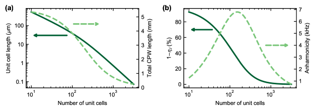
Given an initial resonance frequency for zero bias current of and the CPW parameters as specified in the main text for a wide CPW, we can use Eq. (S17) to calculate the relation between unit cell length and number of unit cells, cf. Fig.S12(a). Compared to the device in the main text, the JJ CPW can be significantly shorter, e.g. for a unit cell length . The higher the number of unit cells, the shorter the individual unit cells, which leads to an increase in the participation ratio of the Josephson inductance to the total inductance per unit cell,
| (S35) |
and the smaller the contribution of normal inductance , cf. Fig.S12(b). The anharmonicity has a maximum of for a unit cell number which corresponds to , but drops rapidly for larger .
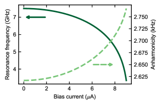
Motivated by a larger current responsivity for large , our proposed device has 845 unit cells and . All parameters are detailed in Tab. SIII. We plot the calculated resonance frequency and anharmonicity for the proposed device design in Fig. 5 from the main text as a function of bias current in Fig. S13. Since Josephson inductance dominates, resulting in the resonance frequency tuning by more than .
| Symbol | Description | Value |
|---|---|---|
| CPW center conductor | ||
| CPW gaps to ground | ||
| Base layer thickness | ||
| Unit cell length | ||
| Number of unit cells | 845 | |
| total CPW length | ||
| Josephson inductance per unit cell | ||
| Normal inductance per unit cell | ||
| Geometric capacitance per unit cell |
SXI.2 Analytical model in the limit of large
We now study the fundamental mode () of an array with many unit-cells (). By Taylor expanding the cosine of Eqs. (S17) and (S30), the fundamental mode frequency and derivative of the admittance are then given by
| (S36) | ||||
| (S37) |
The quantity which relates zero-point fluctuations in phase accross the th unit cell to the zero-point fluctuations of the first unit-cell can be simplified to
| (S38) |
Plugging these quantities into the expression of the anharmonicity, leads to
| (S39) | ||||
| (S40) |
where is the reduced flux quantum and we made use of the relation .
SXI.3 Alternative derivation
We assume that the fundamental cavity mode of the JJ array CPW has current antinodes at both ends, i.e. we are dealing with a cavity such that the resonator length with the resonance wavelength . The resonance frequency of the fundamental mode dependent on and is given by
| (S41) |
which is equivalent to Eq. (S36). For given , , , and , this allows for the calculation of the needed unit cell length .
As we are working with a half-wavelength mode, the basic relation between the resonance frequency and the zero-point fluctuation flux per length in the limit of a continuous flux distribution is given by
| (S42) |
where and is the flux per length of transmission line. This corresponds to
| (S43) |
Hence, the flux of the th junction is approximately given by
| (S44) |
where the first factor takes into account that only part of the flux is across the junction. With the Josephson energy , the anharmonicity is given by
| (S45) | ||||
| (S46) | ||||
| (S47) |
where we have used the fact that the cosine sum for values is equal to , which is identical to the result of the full analytical model in the limit of large , cf. Eq. (S40).