Single artificial atoms in silicon emitting at telecom wavelengths
Given its unrivaled potential of integration and scalability, silicon is likely to become a key platform for large-scale quantum technologies. Individual electron-encoded artificial atoms either formed by impurities he_two-qubit_2019 or quantum dots watson_programmable_2018 ; maurand_cmos_2016 have emerged as a promising solution for silicon-based integrated quantum circuits. However, single qubits featuring an optical interface needed for large-distance exchange of information hensen_loophole-free_2015 have not yet been isolated in such a prevailing semiconductor. Here we show the isolation of single optically-active point defects in a commercial silicon-on-insulator wafer implanted with carbon atoms. These artificial atoms exhibit a bright, linearly polarized single-photon emission at telecom wavelengths suitable for long-distance propagation in optical fibers. Our results demonstrate that despite its small bandgap ( eV) a priori unfavorable towards such observation weber_quantum_2010 , silicon can accommodate point defects optically isolable at single scale, like in wide-bandgap semiconductors aharonovich_solid-state_2016 . This work opens numerous perspectives for silicon-based quantum technologies, from integrated quantum photonics to quantum communications wehner_quantum_2018 and metrology.
Capitalizing on the great success of the microelectronics industry, silicon is undoubtedly a promising platform for deploying large-scale quantum technologies. Silicon-based electrical qubits associated either to individual dopants he_two-qubit_2019 or to gate-defined quantum dots watson_programmable_2018 ; maurand_cmos_2016 , have already been used to demonstrate the elementary building blocks towards scalable integrated quantum circuits. Besides requiring operation in a dilution fridge, those matter qubits are still not able to remotely exchange quantum information at long distances because they are not interfaced with optical light. On the other side, photonic qubits at telecom wavelengths can be generated inside silicon by probabilistic non-linear optical processes qiang_large-scale_2018 . Even if they are adapted to long-distance propagation, those photons are not coupled to matter quantum systems, thus limiting the implementation of scalable silicon quantum photonics silverstone_silicon_2016 . Another type of quantum systems that can fill the gap but is still lacking in this industry-friendly platform are optically-active spin defects, that combines an optical interface with a solid-state medium to encode quantum information awschalom_quantum_2018 . A sine qua non condition to develop such spin-photon interfaces is first to demonstrate that individual point defects can be optically isolated in silicon.
Deep-level point defects in semiconductors feature electronic states buried inside the bandgap of the material aharonovich_solid-state_2016 . Under laser illumination, some of these defects behave as artificial solid-state atoms offering multiple quantum functionalities awschalom_quantum_2018 . Diamond has been the pioneering platform for the detection and control of individual point defects gruber_scanning_1997 , which can be used as single-photon sources for quantum cryptography beveratos_single_2002 , spin-photon interfaces for quantum networks hensen_loophole-free_2015 or high-sensitivity quantum sensors gross_real-space_2017 to name a few. In the last years, optically-active point defects have been detected at single scale in a large variety of wide-bandgap materials aharonovich_solid-state_2016 , thus offering to extend such experiments on novel platforms better suited to industrial processes. Despite its ubiquity in the microelectronics industry, silicon was until now still absent of the list. Owing to its narrow bandgap ( eV), it was an open question whether or not this semiconductor could accommodate optically-active single defects with electronic states well-isolated from its valence and conduction bands weber_quantum_2010 . Here we give a positive answer to this question by demonstrating the isolation of individual photoluminescent point defects hosted in the silicon matrix. These defects exhibit several striking features including (i) linearly polarized single-photon emission at telecom wavelengths, (ii) long-term photostability, and (iii) high brightness.
The studied sample consists of a commercial 220-nm-thick silicon-on-insulator (SOI) wafer implanted with -keV carbon ions at a fluence of cm-2 in view of creating carbon-related defects davies_optical_1989 ; beaufils_optical_2018 (see Methods for details). The photoluminescence (PL) response of this carbon-implanted SOI sample was studied with a scanning confocal microscope optimized for near-infrared spectroscopy at cryogenic temperature. Optical excitation was performed far above the silicon bandgap with a 532-nm continuous laser focused onto the sample through a high numerical aperture microscope objective (NA = 0.85). The PL signal was collected by the same objective and directed either to a spectrometer or to fiber-coupled infrared single-photon detectors featuring a quantum efficiency (see Methods for details).
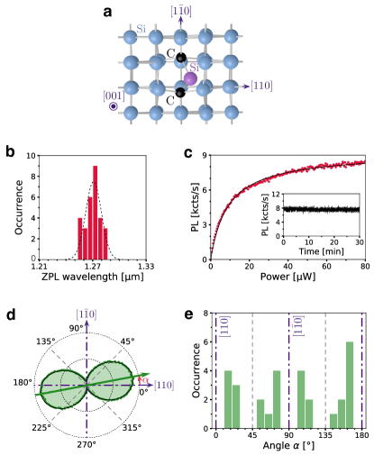
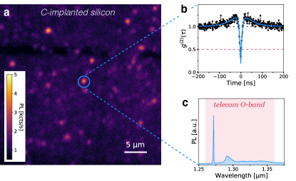
Figure 1a depicts a typical PL raster scan of the silicon sample recorded at 10 K, which reveals bright diffraction-limited PL spots. To demonstrate that they correspond to individual artificial atoms, the resulting photon emission statistics was systematically analyzed by measuring the second-order correlation function with two infrared single photon detectors mounted in a Hanbury-Brown and Twiss configuration. As shown in Figure 1b, a clear antibunching is observed at zero delay, , which is a fingerprint of single-photon emission from an individual quantum emitter. The deviation from an ideal single-photon emission, i.e. , is well explained by residual background photons and detector dark counts beveratos_room_2002 . This constitutes the first observation of single optically-active point defects embedded in the silicon lattice.
Besides their isolation at single scale, a further asset of such emitters is that their PL spectrum falls into the O-band of optical telecommunications, with a sharp zero-phonon-line (ZPL) at a wavelength around m followed by a broad phonon sideband (Fig. 1c). The Debye-Waller factor, corresponding to the proportion of photons emitted into the ZPL, reaches about . Such a PL spectrum is very similar to the one produced by dense ensembles of G-centers in silicon davies_optical_1989 ; beaufils_optical_2018 ; Thewalt . We thus attribute the observed single emitters in the telecom O-band to individual G-centers in silicon. Even though the precise structure of this defect still remains under debate docaj_three_2012 ; wang_g-centers_2014 ; timerkaeva_structural_2018 , it is now widely accepted as being made of a pair of carbon atoms bridging an interstitial silicon atom song_bistable_1988 ; capaz_theory_1998 (Fig. 2a). The C-Si-C complex has a conformation resembling a water molecule, with a (C-Si-C) angle of (see Methods for details). We note that PL spectra recorded for a set of 29 single G-centers indicate variations of the ZPL wavelength (Fig. 2b). A Gaussian fit of the corresponding distribution gives a standard deviation of nm. This observation likely results from local strain-induced effects, as already reported for large ensembles of G-centers under uniaxial stress tkachev_piezospectroscopic_1978 .
The G-center shows several appealing properties in the prospect of developing integrated single-photon sources in silicon. Besides an emission at telecom wavelengths, individual G-centers exhibit a long-term stability under optical illumination, showing neither blinking nor bleaching effects (Fig. 2c Inset), and are robust against repeated thermal cycles from 10 K to room temperature. Furthermore, this defect is particularly bright under green laser illumination. A typical PL saturation curve recorded for a single G-center is shown in Figure 2c. A maximum counting rate around cts/s can be obtained at saturation, despite (i) the high refractive index of silicon () leading to total internal reflection at the silicon-air interface and (ii) the low quantum efficiency of our infrared single-photon detectors (). Significant improvements of the detected PL signal could be easily obtained in future by using superconducting single photon detectors and/or by integrating G-centers into silicon photonic structures schmitt_observation_2015 ; cueff_tailoring_2019 . Last, the G-center features a linearly-polarized single-photon emission. Figure 2d shows a typical emission polarization diagram recorded by rotating a polarizer in front of the single-photon detectors. The observed PL modulation with a contrast close to unity indicates that the G-center behaves as a single emitting dipole, whose projection on the (001)-oriented silicon surface is here lying at from the [110] crystal axis. A systematic analysis over a set of 29 single G-centers reveals that the emission dipoles are pointing in specific directions distributed across four subgroups, which exclude the [110] and [10] axis (Fig. 2e). These preferential directions are attributed to the different orientations of the G-center in the silicon matrix lee_optical_1982 .
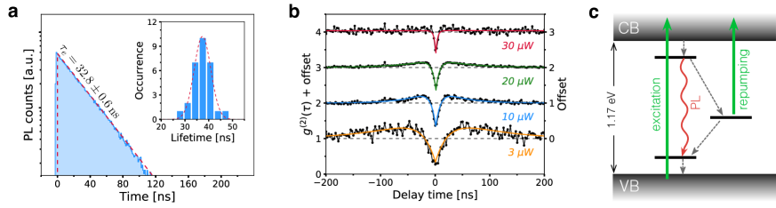
To gain insights into the dynamics of optical cycles, time-resolved PL measurements were performed with a pulsed-laser excitation at 532 nm. As shown in Figure 3a, the PL decay is well fitted by a mono-exponential function providing the lifetime of the excited level. Measurements performed for several single G-centers indicate fluctuations of the excited-level lifetime (Fig. 3a Inset). The resulting statistics is well-described by a Gaussian distribution with a mean value ns and a standard deviation ns. No correlation could be found between the lifetime of the excited level and neither the shift of the ZPL wavelength nor the emission dipole orientation. We note a significant discrepancy with the value recently reported for ensembles of G-centers ( ns) beaufils_optical_2018 . This variation could originate from changes in the dynamics involving different charge states or defect conformations song_bistable_1988 when G-centers are either isolated or inside dense ensembles. A similar effect was recently reported for nitrogen-vacancy (NV) defects in diamond, whose excited-level lifetime decreases from ns for a single defect hosted in an ultrapure diamond matrix down to ns for dense NV ensembles in a diamond sample heavily doped with nitrogen Manson_2018 .
Further informations can be obtained by analyzing the evolution of the second-order correlation function with the laser excitation power (Fig. 3b). A photon bunching effect () is observed at low power, revealing that optical cycles involve non-radiative relaxation processes through a metastable level beveratos_room_2002 . Interestingly, this effect gradually disappears while increasing the laser power, until the function mimics the dynamics of a pure two-level system (top trace in Fig. 3b). This peculiar behavior can be explained by considering a photo-induced repumping mechanism from the metastable level to the excited level (Fig. 3c). This process likely contributes to the high brightness of single G-centers under green laser illumination.
The isolation of single point defects emitting at telecom wavelengths in silicon provides numerous opportunities for integrated quantum technologies.
First, these single-photon emitters could be integrated in photonic circuits fabricated by industrial-grade and CMOS-compatible processes silverstone_silicon_2016 . Full processing of photonic qubits from their deterministic generation to their measurement with integrated single-photon detectors could then be achieved on a silicon chip. Coupling these individual emitters to highly mature silicon-based nanomechanical systems riedinger_remote_2018 could also open new pathways in hybrid quantum optomechanics. Finally, a remaining challenge is to assess if the internal spin degree of freedom of a single G-center in silicon can be monitored through optical detection of the magnetic resonance, as reported a long time ago for ensembles of G-centers lee_optical_1982 .
The resulting spin-photon interface at telecom wavelengths would open large prospects for long-distance fibered-based quantum networks wehner_quantum_2018 and quantum metrology.
References
- (1) He, Y. et al. A two-qubit gate between phosphorus donor electrons in silicon. Nature 571, 371 (2019).
- (2) Watson, T. F. et al. A programmable two-qubit quantum processor in silicon. Nature 555, 633–637 (2018).
- (3) Maurand, R. et al. A CMOS silicon spin qubit. Nature Communications 7, 13575 (2016).
- (4) Hensen, B. et al. Loophole-free Bell inequality violation using electron spins separated by 1.3 kilometres. Nature 526, 682–686 (2015).
- (5) Weber, J. R. et al. Quantum computing with defects. Proceedings of the National Academy of Sciences 107, 8513–8518 (2010).
- (6) Aharonovich, I., Englund, D. & Toth, M. Solid-state single-photon emitters. Nature Photonics 10, 631–641 (2016).
- (7) Wehner, S., Elkouss, D. & Hanson, R. Quantum internet: A vision for the road ahead. Science 362, eaam9288 (2018).
- (8) Qiang, X. et al. Large-scale silicon quantum photonics implementing arbitrary two-qubit processing. Nature Photonics 12, 534 (2018).
- (9) Silverstone, J. W., Bonneau, D., O’Brien, J. L. & Thompson, M. G. Silicon Quantum Photonics. IEEE Journal of Selected Topics in Quantum Electronics 22, 390–402 (2016).
- (10) Awschalom, D. D., Hanson, R., Wrachtrup, J. & Zhou, B. B. Quantum technologies with optically interfaced solid-state spins. Nature Photonics 12, 516–527 (2018).
- (11) Gruber, A. et al. Scanning confocal optical microscopy and magnetic resonance on single defect centers. Science 276, 2012–2014 (1997).
- (12) Beveratos, A. et al. Single Photon Quantum Cryptography. Physical Review Letters 89, 187901 (2002).
- (13) Gross, I. et al. Real-space imaging of non-collinear antiferromagnetic order with a single-spin magnetometer. Nature 549, 252–256 (2017).
- (14) Davies, G. The optical properties of luminescence centres in silicon. Physics Reports 176, 83–188 (1989).
- (15) Beaufils, C. et al. Optical properties of an ensemble of G-centers in silicon. Physical Review B 97, 035303 (2018).
- (16) Beveratos, A. et al. Room temperature stable single-photon source. The European Physical Journal D 18, 191–196 (2002).
- (17) Chartrand, C. et al. Highly enriched reveals remarkable optical linewidths and fine structure for well-known damage centers. Phys. Rev. B 98, 195201 (2018).
- (18) Docaj, A. & Estreicher, S. K. Three carbon pairs in Si. Physica B: Condensed Matter 407, 2981–2984 (2012).
- (19) Wang, H., Chroneos, A., Londos, C. A., Sgourou, E. N. & Schwingenschlegl, U. G-centers in irradiated silicon revisited: A screened hybrid density functional theory approach. Journal of Applied Physics 115, 183509 (2014).
- (20) Timerkaeva, D., Attaccalite, C., Brenet, G., Caliste, D. & Pochet, P. Structural, electronic, and optical properties of the C-C complex in bulk silicon from first principles. Journal of Applied Physics 123, 161421 (2018).
- (21) Song, L. W., Zhan, X. D., Benson, B. W. & Watkins, G. D. Bistable defect in silicon:the interstitial-carbon-substitutional-carbon pair. Physical Review Letters 60, 460–463 (1988).
- (22) Capaz, R. B., Dal Pino, A. & Joannopoulos, J. D. Theory of carbon-carbon pairs in silicon. Physical Review B 58, 9845–9850 (1998).
- (23) Tkachev, V. D. & Mudryi, A. V. Piezospectroscopic effect on zero-phonon luminescence lines of silicon. Journal of Applied Spectroscopy 29, 1485–1491 (1978).
- (24) Schmitt, S. W., Sarau, G. & Christiansen, S. Observation of strongly enhanced photoluminescence from inverted cone-shaped silicon nanostructures. Scientific Reports 5, 17089 (2015).
- (25) Cueff, S. et al. Tailoring the Local Density of Optical States and Directionality of Light Emission by Symmetry Breaking. IEEE Journal of Selected Topics in Quantum Electronics 25, 1–7 (2019).
- (26) Lee, K. M., O’Donnell, K. P., Weber, J., Cavenett, B. C. & Watkins, G. D. Optical Detection of Magnetic Resonance for a Deep-Level Defect in Silicon. Physical Review Letters 48, 37–40 (1982).
- (27) Manson, N. B. et al. - pair centre in 1b diamond. New Journal of Physics 20, 113037 (2018).
- (28) Riedinger, R. et al. Remote quantum entanglement between two micromechanical oscillators. Nature 556, 473–477 (2018).