Theoretical study of structure and magnetism of Ga1-xVxSb compounds for spintronic applications
Abstract
In this paper, the structural, electronic and magnetic properties of Zinc-blende Ga1-xVxSb compounds, with from dilute doping situation to extreme doping limiting, were systematically investigated by first-principles calculations. V atoms prefer to substitute the Ga atoms and the formation energy is lower in Sb-rich than Ga-rich growth condition. Meantime, the SbGa antisite defects can effectively decrease the energy barrier of substitution process, from 0.85 eV to 0.53 eV. The diffusion of V atom in GaSb lattice is through meta-stable interstitial sites with an energy barrier of 0.6 eV. At a low V concentration = 0.0625, V atoms prefer a homogeneous distribution and an antiferromagnetic coupling among them. However, starting from = 0.5, the magnetic coupling among V atoms changes to be ferromagnetic, due to enhanced superexchange interaction between and states of neighbouring V atoms. At the extreme limiting of = 1.00, we found that Zinc-blende VSb as well as its analogs VAs and VP are intrinsic ferromagneitc semiconductors, with a large change of light absorption at the curie temperature. These results indicate that Ga1-xVxSb compounds can provide a platform to design the new electronic, spintronic and optoelectronic devices.
pacs:
75.50.Pp, 71.20.-b, 75.30.-m, 75.10.DgThe materials with both semiconducting behavior and robust magnetism provide the chance for utilizing the charge and the spin characters of electrons simultaneously, which offers the possibility to combine logic elements and data storage in the same device. Žutić, Fabian, and Das Sarma (2004); Jungwirth et al. (2006a); Sanvito, Theurich, and Hill (2002); Sato et al. (2010) Diluted magnetic semiconductors, which was realized in group III-V and II-VI compounds by doping transition metal ions, Jungwirth et al. (2006b); Dietl and Ohno (2001) have limitations such as small net magnetization, uncontrollable dopant distribution and low Curie temperature (). Žutić, Fabian, and Das Sarma (2004); Jungwirth et al. (2006a) Thus, intrinsic magnetic semiconductors are more favored for the development of spintronics devices. At present, semiconductor spintronics is at a fascinating stage and expects to important material developments. Dietl and Ohno (2006)
Gallium antimonide (GaSb) is a group III-V semiconductor with the zinc-blende (ZB) crystal lattice and many promising properties. With small effective mass and high carrier mobility, GaSb is thought to be candidate materials in metal-oxide-semiconductor devices Yokoyama et al. (2016) and high-speed infrared photodetectors. Sun et al. (2019) Its direct band gap can be significantly narrowed by replacing Sb with just a small fraction (around 1%) of nitrogen. Virkkala et al. (2012) Furthermore, GaSb is a suitable substrate for growing other ternary and quaternary III-V compounds, due to good lattice matching. Dutta, Bhat, and Kumar (1997) The introduction of defects or dopants has a large influence on the properties of GaSb. Tu et al. experimentally demonstrated that Fe-doped GaSb is a p-type ferromagnetic (FM) semiconductor with of 340 K at a Fe doping concentration of 25%. Tu et al. (2016) Lin et al. predicted that the magnetic coupling among CrGa and CrSb substitution are ferromagnetic in Cr-doped GaSb. Lin et al. (2019) Wang et al. predicted that Mn-doped GaSb exhibit ferromagnetic half-metallic properties for different dopant concentrations. Wang et al. (2019) The inducing of vanadium (V) into GaSb was initiated to produce semi-insulating III-V compounds several years ago. Bilel et al. (2015) Bchetnia et al. found that V has a low diffusion coefficient and diffuses via interstitial sites in bulk GaAs. Bchetnia et al. (2004) Huang et al predicted that tetrahedral semiconductors can be FM due to strong superexchange interactions. Huang et al. (2019) Because the experiments on V-doped GaSb are still limited, the energetics and dynamics of V dopants in bulk GaSb at different V concentrations are not clear, which are critical in determining the performance of devices based on V-doped GaSb.
In this work, we have studied the structural, electronic and magnetic properties of Ga1-xVxSb compounds by the first-principles calculations. The computational details are given in the supplementary materials. The preferred occupation, magnetic configuration and diffusion pattern of V atom were identified for the dilute V situation. Then we unveiled a magnetic phase transition from antiferromagnetic (AFM) to FM states in Ga1-xVxSb as V content increases and analyse the underling mechanism. At the extreme =1.0, we predicted that ZB VSb, as well as VP and VAs, are intrinsic FM semiconductors.
| Position | Ga-rich | Sb-rich | ||
|---|---|---|---|---|
| NM | M | NM | M | |
| 2.394 | 0.291 | 2.070 | -0.03 | |
| 3.019 | 1.810 | 3.343 | 2.134 | |
| 2.738 | 0.852 | 2.738 | 0.852 | |
| 3.428 | 1.392 | 3.428 | 1.392 | |
| 2.680 | 0.898 | 2.680 | 0.898 | |
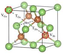
Firstly, we calculated the lattice constants of bulk V. Considered the strong correlation effects of V- orbitals, we applied the LDA + U scheme including an effective onsite repulsion Uf = 2.7 eV. Pickett, Erwin, and Ethridge (1998) The obtained is 3.04 Å, consistent with the experimental values of 3.03 Å. Haynes (2014) On the contrast, the with Uf = 0 eV is 2.98 Å. Next, we put a single V atom into a cubic supercell with 64 atoms to simulate a dilute doping situation when the V atom can be seen as an isolated impurity. The formation energy of different nonequivalent doping sites of V were examined in Ga-rich or Sb-rich growth condition (see the supplementary materials). As shown in Fig. 1, these positions include the substitution of Ga atom () or Sb atom (), tetrahedral site coordinated with four Ga () or Sb () atoms, hexagonal (), bond-center () site. A Frenkel defect (), in which a V atom occupies the Ga site and repels original Ga atom to an adjacent site, was also considered. Both magnetic and non-magnetic states of V atom were considered.
We found that the V atom on Hex site and B site are not stable. They will transfer to and configuration, respectively. The of stable configurations are shown in Table. 1. The V atom in GaSb prefers to substitute the Ga site () in the magnetic state, and the is smaller in Sb-rich than Ga-rich growth condition. That is consistent with the experiment where the atomic percentage of Sb is higher than that of Ga in the region with vanadium precipitated. Hidalgo et al. (1998) We also calculated the of single V dopant in GaSb with Uf = 0 eV and Uf = 3.5 eV. The results also show that the is the most stable doping configuration, as shown in Fig. S1.
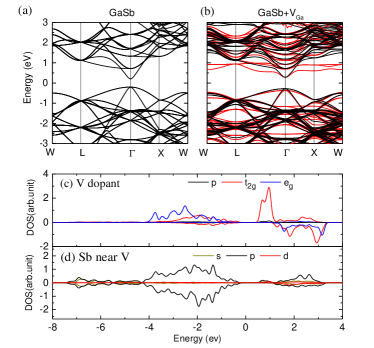
The band structures for pristine GaSb and single V-doped GaSb are displayed in Fig. 2(a) and 2(b). The bands with V component are located in both the valence bands and conduction bands, which is consistent with the experiment that no deep levels were found in the band gap in V-doped GaSb. Lauer et al. (1997) Compared with pristine GaSb, the band gap of dilute V-doped was enlarged from 0.40 eV to 0.54 eV. Due to the local tetrahedral crystalline field, the 3 orbitals of V atom are split to lower double degenerated ( and ) orbitals and higher three-fold degenerated (, , and ) orbitals. The PDOS of V- and orbitals have partly overlap in valence bands (see Fig. 2(c)). Meanwhile, the PDOS of spin-up and spin-down orbitals are separated and located at the valence bands and conduction bands. Thus, the exchange splitting is larger than the crystalline field splitting in V-doped GaSb. The orbitals of V atom hybridize with the 5 orbitals of surrounding Sb atoms (see Fig. 2(d)), while the V- orbitals are localized due to th weak hybridization with the Se- orbitals as a result of the incompatible symmetry between them. Sanyal, Bergqvist, and Eriksson (2003) The asymmetric PDOS of orbitals create a magnetic moment of 2.340 per V atom. The neighboring Sb atoms carry a total negative magnetic moment of -0.312 , respectively. Thus, the coupling between the spin of V atom and neighbouring Sb atoms is AFM.
The direct diffusion pathway of V atom in GaSb can proceed through interstitial sites along a trajectory (see Fig. 1). The interstitial and site are meta-stable positions. V atom has a higher in site than in site, due to larger repulsion from negative Sb ions with larger ion radius (see table. 1). The diffusion barrier is estimated to be about 0.60 eV (see Fig. 3(a)) by Nudged Elastic Band (NEB) method, Mills, Jónsson, and Schenter (1995) which is smaller than that of V diffusion in GaAs (1.51 eV) Bchetnia et al. (2004) and GaN ( eV). Bchetnia et al. (2009)
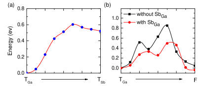
Seen from Fig. 1, a V atom at the site can kicks a Ga atom out of its equilibrium position to an adjacent site, and substitute the Ga vacancy. By NEB methods, we estimated that energy barrier to overcome during such a substitution process was 0.85 eV (see Fig. 3(b)). However, the intrinsic defects of GaSb will affect the V substitution process. The main defect in Sb-rich growth condition was SbGa antisite that a Sb occupies the Ga site. Buckeridge et al. (2019) When a V atom is at the site and a nearby SbGa antisite appears at the same time, the extra repulsion from SbGa antisite makes the V substitution process occur more easily, as the barrier was decreased to be 0.53 eV through the NEB calculations. Thus, Sb-rich growth condition is favored for the V substitution of Ga, due to the decrease of both of VGa and barrier of V substitution process.
When the V content increases, magnetic coupling among local magnetic moments of different V atoms have to be considered. By substituting more Ga atoms by V atoms in GaSb supercell, we simulated the Ga1-xVxSb compounds at = 0.0625, 0.25, 0.5, 0.75 and 1.00. It is possible to prepare materials with high enough dopant concentration by employing thermal nonequilibrium preparation mechanisms, such as the growth of thin films and spinodal decomposition. Dietl and Ohno (2006) The current model is mainly used as a theoretical model to demonstrate the existence of magnetic phase transition in Ga1-xVxSb compounds as the V content increases, which is expected to be observed in the experiment.
We introduced two defects into the 64-atom supercell, which corresponds to . We considered the NM, FM and AFM states for different structures, and calculated the corresponding total energy. Meanwhile, we also examined the GaSb supercell with a and a defect, and found that it have an energy eV higher than that of configurations with two defects. We calculated the total energy as a function of V separation which presents the distance between V atoms at the reference 0 site and the th site (see Fig. 4(a)). The magnetic coupling will occur between V atoms, because both FM or AFM states have lower energy than NM states. The stable configuration is AFM state even for two with a long distance. That is consistent with previous work which predicted that V-V exchange coupling constants in III-V compounds were negative at a long distance, using Korringa-Kohn-Rostoker coherent potential approximation (KKR-CPA) Green s function method. Belhadji et al. (2007)
The AFM coupling between V at low doping region is similar to the AFM coupling of Co in ZnO. Sati et al. (2007) In AFM states, the spin orientation of the V atoms and neighbouring Se atoms is opposite (see Fig. S2). The representative PDOS of , as displayed in Fig. S3 (a), indicates that Ga1-xVxSb compounds is semiconducting at . Moreover, the energy difference between different AFM configurations is less than 0.015 eV, indicating that V atoms tend to distribute homogeneously at low V concentrations. We also performed the same calculations with Uf = 0 eV and Uf = 3.5 eV. The obtained results also indicate the stable magnetic coupling between defect is AFM, as shown in Fig. S4.
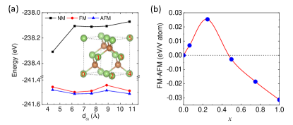
By substituting more Ga by V atoms in GaSb supercells, we simulated the Ga1-xVxSb compounds at = 0.25, 0.50, 0.75 and 1.00. For each value, a number of initial geometrical configurations in NM, FM and AFM states were fully relaxed to distinct stable structures. We selected the one with the lowest energy at each under study. These lowest-energy structures are shown in Fig. S5. As NM states have much higher energy, Fig. 4(b) only shows the energy difference between the FM and AFM states in most state structures at each . As the V content increases to be above 0.5, the ground-state magnetic ordering of Ga1-xVxSb changes from AFM to FM. Thus, there is a competition between the FM and AFM state of Ga1-xVxSb at different V content .
As Ga1-xVxSb compounds has a band gap (see Fig. S3), the super-exchange interaction dominates its magnetic behavior. Belhadji et al. (2007) Based on the Goodenough-Kanamori-Anderson (GKA) superexchange theory, Goodenough (1955) the bonding angle of the tetrahedral crystal is 109.5∘, which allows both AFM and FM superexchange interaction among V atoms. Compared to the NM state, the energy gain per V atom for AFM coupling is give by Sato et al. (2010)
| (1) |
and the energy gain for FM coupling is give by Sato et al. (2010)
| (2) |
where and are the energy of and levels, respectively. refers to the hopping element between the two states on neighbouring V ions. represents the hopping element between the state and the state on the neighbouring V ions. The is expected to be considerably smaller than the , since the orbitals are localized. But denominator in Eq. 2, which represents the strength of crystalline field splitting, is smaller than that of Eq. 1 which represents the exchange splitting in V-doped GaSb. At small V content, Fig. 4(a) indicates that the is little larger than . Therefore, Ga1-xVxSb compounds prefer the AFM states at = 0.0625. Both and will increase as the increases. Considering the prefactor of Eq. 2 is twice as much as that of Eq. 1, the will become larger than at a critical . The critical is about the 0.5 in our calculation (see Fig. 4(b)). Thus, as the V content increases, the superexchange FM coupling between the state and the state on the neighbouring V atoms dominate the magnetic properties of Ga1-xVxSb compounds and make FM state become the ground state.
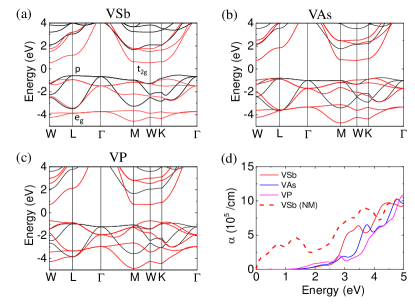
The ZB VSb represents the extreme doping limit of . Though ZB VSb was a meta-stable phase compared to its NiAs-phase, Boochani et al. (2010) it may can be grown epitaxially on some appropriate substrates in the form of sufficiently thick layers. Boochani et al. (2010); Xie, Liu, and Pettifor (2003) The ground state of ZB VSb is in FM state (see Fig. S6). Using more accurate Heyd-Scuseria-Ernzerhof (HSE) hybrid functional, Heyd, Scuseria, and Ernzerhof (2003) the band structure indicates that ZB VSb is FM semiconductors (see Fig. 5(a) and Fig. S7). Around -4 eV, the spin-up V- bands can be seen. They are flat indicating weak hybridization with the orbitals of neighbouring Sb atoms. The next bands are the bonding states of hybridizing between Sb- orbitals and V- orbitals for both spin-up and spin-down electrons. As energies of Sb- orbitals are lower than that of V- orbitals, the contribution of Sb- to bonding state is larger than that of V-. The corresponding anti-bonding states are located in conduction bands. The valence band maximum at the point and conduction band minimum at the point are mainly from the spin-down Sb- orbitals and spin-up V- orbitals, respectively. We expanded the current calculations to other analogs including ZB VAs and VP which are also FM semiconductors (see Fig. 5).
We adopted Heisenberg Hamiltonian to describe these FM VX (X = Sb, As and P) (see the computational details in the supplementary materials.). The exchange interactions and are obtained by the relations between energy and spin configuration (see Figure S8 and Table. S1). By MC simulations, the Tc was estimated to be about 100, 400 and 650 K for ZB VSb, VAs, and VP, respectively (see Fig. S9). The high Tc of ZB VP is consistent with previous work. Huang et al. (2019)
At last, we found that VX (X = Sb, As and P) happen a semiconductor-to-metal transition between the FM and NM state through the band calculations. As a result, the absorption coefficient Gajdoš et al. (2006) of VX present a large difference at Tc (see Fig. 5(d)), which indicates their potential applications in switching and sensor devices.
In summary, we have investigated the structure and magnetism of Ga1-xVxSb compound by first-principles calculations. V atoms are likely to substitute the Ga atoms in Sb-rich growth condition, due to the smaller formation energy and smaller barrier of substitution process with the help of antisite SbGa defects. The diffusion of V atom is through a THexTSb trajectory with a barrier of 0.60 eV. At low doping concentrations, V atoms prefer to form a homogeneous distribution with antiferromagnetic coupling. However, the magnetic coupling among V dopants changes to ferromagnetic when the V content increases to be above 0.50. The enhanced superexchange interaction between and orbitals of neighbouring V atoms dominates the magnetic ground state at high V content. At the extreme =1.0, Zinc-blende VSb as well as VAs and VP are ferromagnetic semiconductors. Their absorption abilities happen a large change at Curie temperature, which is desirable for switching and sensor application. These results provide a guide for further experimental study and the design of new spintronic and optoelectronic devices.
Acknowledgements.
This work was supported by National Natural Science Foundation of China (No.11904313), the Project of Hebei Educational Department, China (No.ZD2018015 and QN2018012), the Natural Science Foundation of Hebei Province (No.A2019203507), and the Doctor foundation project of Yanshan University (No.BL19008).References
- Žutić, Fabian, and Das Sarma (2004) I. Žutić, J. Fabian, and S. Das Sarma, Rev. Mod. Phys. 76, 323–410 (2004).
- Jungwirth et al. (2006a) T. Jungwirth, J. Sinova, J. Mašek, J. Kučera, and A. H. MacDonald, Rev. Mod. Phys. 78, 809–864 (2006a).
- Sanvito, Theurich, and Hill (2002) S. Sanvito, G. Theurich, and N. A. Hill, J. Supercond. 15, 85–104 (2002).
- Sato et al. (2010) K. Sato, L. Bergqvist, J. Kudrnovský, P. H. Dederichs, O. Eriksson, I. Turek, B. Sanyal, G. Bouzerar, H. Katayama-Yoshida, V. A. Dinh, T. Fukushima, H. Kizaki, and R. Zeller, Rev. Mod. Phys. 82, 1633–1690 (2010).
- Jungwirth et al. (2006b) T. Jungwirth, J. Sinova, J. Mašek, J. Kučera, and A. H. MacDonald, Rev. Mod. Phys. 78, 809–864 (2006b).
- Dietl and Ohno (2001) T. Dietl and H. Ohno, Physica E 9, 185 – 193 (2001).
- Dietl and Ohno (2006) T. Dietl and H. Ohno, Mater. Today 9, 18 – 26 (2006).
- Yokoyama et al. (2016) M. Yokoyama, H. Yokoyama, M. Takenaka, and S. Takagi, Appl. Phys. Lett. 109, 213505 (2016).
- Sun et al. (2019) J. Sun, M. Peng, Y. Zhang, L. Zhang, R. Peng, C. Miao, D. Liu, M. Han, R. Feng, Y. Ma, Y. Dai, L. He, C. Shan, A. Pan, W. Hu, and Z.-X. Yang, Nano Lett. 19, 5920–5929 (2019), pMID: 31374165.
- Virkkala et al. (2012) V. Virkkala, V. Havu, F. Tuomisto, and M. J. Puska, Phys. Rev. B 85, 085134 (2012).
- Dutta, Bhat, and Kumar (1997) P. S. Dutta, H. L. Bhat, and V. Kumar, J. Appl. Phys. 81, 5821–5870 (1997).
- Tu et al. (2016) N. T. Tu, P. N. Hai, L. D. Anh, and M. Tanaka, Appl. Phys. Lett. 108, 192401 (2016).
- Lin et al. (2019) X. Lin, F. Pan, H. Chen, and Z. Cao, Jpn. J. Appl. Phys. 58, 083003 (2019).
- Wang et al. (2019) C. Wang, W. Wan, Y. Ge, Y.-H. Zhao, K. Zhang, and Y. Liu, Physica B 572, 225 – 229 (2019).
- Bilel et al. (2015) C. Bilel, H. Fitouri, I. Zaied, A. Bchetnia, A. Rebey, and B. E. Jani, Mater. Sci. Semicond. Process. 31, 100 – 105 (2015).
- Bchetnia et al. (2004) A. Bchetnia, M. Souissi, A. Rebey, and B. E. Jani, J. Cryst. Growth 270, 376 – 379 (2004).
- Huang et al. (2019) C. Huang, J. Feng, J. Zhou, H. Xiang, K. Deng, and E. Kan, J. Am. Chem. Soc. 141, 12413–12418 (2019).
- Pickett, Erwin, and Ethridge (1998) W. E. Pickett, S. C. Erwin, and E. C. Ethridge, Phys. Rev. B 58, 1201–1209 (1998).
- Haynes (2014) W. M. Haynes, CRC handbook of chemistry and physics (CRC press, 2014).
- Hidalgo et al. (1998) P. Hidalgo, B. Méndez, P. S. Dutta, J. Piqueras, and E. Dieguez, Phys. Rev. B 57, 6479–6484 (1998).
- Lauer et al. (1997) S. Lauer, A. N. Danilewsky, J. Meinhardt, R. Hofmann, A. Dörnen, and K. W. Benz, Cryst. Res. Technol. 32, 1095–1102 (1997).
- Sanyal, Bergqvist, and Eriksson (2003) B. Sanyal, L. Bergqvist, and O. Eriksson, Phys. Rev. B 68, 054417 (2003).
- Mills, Jónsson, and Schenter (1995) G. Mills, H. Jónsson, and G. K. Schenter, Surf. Sci. 324, 305 – 337 (1995).
- Bchetnia et al. (2009) A. Bchetnia, C. Saidi, M. Souissi, T. Boufaden, and B. E. Jani, Semicond. Sci. Technol. 24, 095020 (2009).
- Buckeridge et al. (2019) J. Buckeridge, T. D. Veal, C. R. A. Catlow, and D. O. Scanlon, Phys. Rev. B 100, 035207 (2019).
- Belhadji et al. (2007) B. Belhadji, L. Bergqvist, R. Zeller, P. H. Dederichs, K. Sato, and H. Katayama-Yoshida, J. Phys.: Condens. Matter 19, 436227 (2007).
- Sati et al. (2007) P. Sati, C. Deparis, C. Morhain, S. Schäfer, and A. Stepanov, Phys. Rev. Lett. 98, 137204 (2007).
- Goodenough (1955) J. B. Goodenough, Phys. Rev. 100, 564–573 (1955).
- Boochani et al. (2010) A. Boochani, M. Abolhasani, M. Ghoranneviss, and M. Elahi, Commun. Theor. Phys. 54, 148–158 (2010).
- Xie, Liu, and Pettifor (2003) W.-H. Xie, B.-G. Liu, and D. G. Pettifor, Phys. Rev. B 68, 134407 (2003).
- Heyd, Scuseria, and Ernzerhof (2003) J. Heyd, G. E. Scuseria, and M. Ernzerhof, The Journal of Chemical Physics 118, 8207–8215 (2003).
- Gajdoš et al. (2006) M. Gajdoš, K. Hummer, G. Kresse, J. Furthmüller, and F. Bechstedt, Phys. Rev. B 73, 045112 (2006).