Experimental Study of Different Silicon Sensor Options for the Upgrade of the CMS Outer Tracker
Abstract
During the high-luminosity phase of the LHC (HL-LHC), planned to start in 2027, the accelerator is expected to deliver an instantaneous peak luminosity of up to cm-2s-1. A total integrated luminosity of or even fb-1 is foreseen to be delivered to the general purpose detectors ATLAS and CMS over a decade, thereby increasing the discovery potential of the LHC experiments significantly. The CMS detector will undergo a major upgrade for the HL-LHC, with entirely new tracking detectors consisting of an Outer Tracker and Inner Tracker. However, the new tracking system will be exposed to a significantly higher radiation than the current tracker, requiring new radiation-hard sensors. CMS initiated an extensive irradiation and measurement campaign starting in 2009 to systematically compare the properties of different silicon materials and design choices for the Outer Tracker sensors. Several test structures and sensors were designed and implemented on 18 different combinations of wafer materials, thicknesses, and production technologies. The devices were electrically characterized before and after irradiation with neutrons, and with protons of different energies, with fluences corresponding to those expected at different radii of the CMS Outer Tracker after fb-1. The tests performed include studies with sources, lasers, and beam scans. This paper compares the performance of different options for the HL-LHC silicon sensors with a focus on silicon bulk material and thickness.
1 Motivation
Finely segmented silicon sensors are used in almost all high energy physics experiments for precision charged particle tracking. Owing to their typical position close to the beam pipe they are subjected to high levels of irradiation by neutral and charged particles. Ionization in the oxide layer and at the interface to the silicon causes changes in the sensor properties. The main type of damage investigated in this paper, however, is due to non-ionizing energy loss (NIEL) in the silicon bulk. Defects with energy levels in the silicon band gap are created by removing silicon atoms from their lattice sites, thereby creating pairs of vacancies and interstitial atoms, which then lead to a number of energy levels due to defect kinetics. Depending on their properties, these energy levels have a threefold impact on basic silicon sensor characteristics [1, 2, 3]:
-
1.
Energy levels close to the middle of the band gap tend to increase the volume leakage current. This raises the power consumption and heat load of a sensor, and consequently increases the electrical noise.
-
2.
Charged defects can modify the effective space charge concentration, which changes the voltage needed to achieve high-field regions in the entire volume of the sensor. Especially for high particle fluences, the electric field in the sensor bulk is altered from a linear dependence on depth to a double junction configuration [4].
-
3.
Some defects act as trapping centers for electrons or holes, thus reducing the amount of charge collected.
The sensors in the current CMS microstrip tracker were produced from float-zone silicon wafers using p+ implants on n-type silicon (p-in-n). They were designed to withstand an integrated luminosity corresponding to 10 years of nominal LHC running ( fb-1). However, during the high-luminosity running phase of the LHC (from around 2026 onwards) [5, 6], the instantaneous luminosity will be increased to 5 cm-2s-1, or even to cm-2s-1 in ultimate scenarios, with the goal of collecting an integrated luminosity of 3000 fb-1 by the end of 2037. This corresponds to a 1 MeV neutron equivalent fluence [1, 7, 8] of cm-2 at the innermost radius of the Outer Tracker (OT) (); therefore sensors optimized for these conditions are needed.
Silicon crystals produced with different growing techniques have been proposed and studied in the past [2]. However, these sensors were produced for a variety of experiments by different vendors, and the corresponding measurements are often challenging to compare because the measurements were taken under different conditions. Therefore, starting in 2009, CMS embarked on an extensive campaign to systematically compare silicon materials, sensor designs, and layout parameters under otherwise identical conditions. The same small silicon sensors and test structures for specific measurements were implemented by one industrial supplier, Hamamatsu Photonics K.K. (HPK) [9], on a variety of silicon wafers differing in bulk material, thickness, production process, and whether the silicon bulk is n- or p-type (polarity). The main objectives of this paper are to address the issues of silicon bulk material and thickness, and to study individual strip parameters before and after irradiation. The outcome of this extensive measurement program was used as input to the decision process for CMS OT sensor specifications.
2 The HL-LHC Upgrade of the CMS Outer Tracker
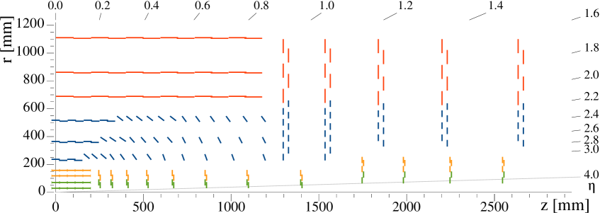
The design concept for the new CMS tracker [6] is based on requirements to maintain efficient tracking capabilities under high-luminosity conditions. With respect to the current tracker, the basic changes are an increased granularity to maintain hit occupancies in the percent range, a reduced material budget in the active region, and delivery of tracker data to the Level 1 (L1) trigger to significantly reduce the input rate to the high-level trigger. Also, radiation tolerant silicon modules that will withstand 10 years of running at the HL-LHC are required. The overall baseline tracker design is shown in Fig. 1. To aid forward jet reconstruction in the presence of a high number of simultaneous proton-proton collisions at each bunch crossing (pileup), the angular coverage of the CMS tracking system is extended significantly up to a pseudorapidity of , mainly by adding forward pixel stations. This will significantly improve the physics performance in key processes such as vector boson fusion and vector boson scattering [6].
CMS [10] adopts a right-handed coordinate system. The origin is centered at the nominal collision point inside the experiment. The axis points towards the center of the LHC, and the axis points vertically upwards. The axis points along the beam direction. The azimuthal angle, , is measured from the axis in the - plane, and the radial coordinate in this plane is denoted by . The polar angle, , is measured from the axis. The pseudorapidity, , is defined as . The momentum transverse to the beam direction, denoted by , is computed from the and components.
The concept of the OT is based on so-called modules, which consist of two closely spaced silicon sensors for an on-module estimate of the transverse momentum of tracks, to be used in the L1 trigger. Hits on the two sensors, which are separated by to depending on the position of the module, are correlated in the front-end chip. This allows the discrimination of high- from low- tracks based on their curvature in the magnetic field of the CMS solenoid. Track “stubs” are formed from the selected correlated clusters in the inner and the outer sensor. These track stubs are used off-detector to build tracks. A module for the outer layers consists of two strip (2S) sensors, while in the inner layers, owing to the higher track density, pixel-strip (PS) modules are used, consisting of a strip sensor and a macro-pixel sensor with long macro-pixels.
The new tracker will use two-phase CO2 cooling to remove the heat generated by the sensors and the electronics. This choice makes it possible to operate and maintain the sensors at or less, thus reducing the power consumption due to the leakage current of the sensors and effectively preventing an increase in the full depletion voltage, , due to reverse annealing. The material budget is also significantly reduced compared to mono-phase liquid cooling. Power losses on the low voltage cables will be reduced by using on-module DC-DC converters.
3 Sensor Specifications for the CMS Outer Tracker
The most important specifications for CMS OT sensors are listed in Table 1. They serve as guidelines for the measurements and results presented in this paper.
The figures before (after) irradiation refer to measurements at () with relative humidity below 60% (below 30%).
| Parameter | Value for 2S | Value for PS |
|---|---|---|
| Depletion voltage* | ||
| Breakdown voltage | ||
| Current density at | ||
| Sensor leakage current at | ||
| Performance after irrradiation | ||
| Target fluence | cm-2 | cm-2 |
| Breakdown voltage at target fluence | ||
| Sensor leakage current at at target fluence | ||
| Minimum signal at target fluence |
*Assuming sensor thicknesses of around for 2S sensors, and for PS sensors.
4 Structures and Wafer Layout
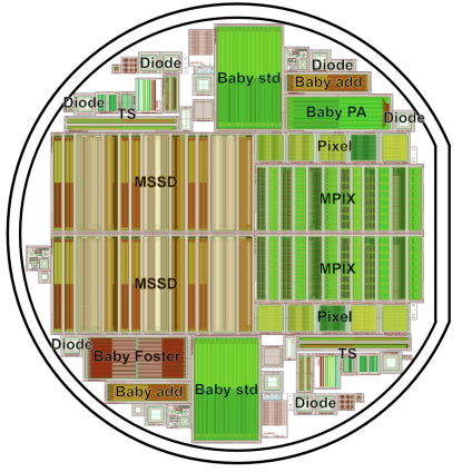
To study the properties of the different materials and production processes before and after irradiation, 28 different structures were specifically designed for this project run (Fig. 2). Several fully functional strip and pixel sensors were implemented. Large areas of the wafer are devoted to structures with different strip and pixel geometries. The remaining part of the wafer was covered with specialized test structures, which give access to parameters that cannot be measured with a sensor. The structures investigated for this paper are pad diodes to study basic material properties (Fig. 3) and AC coupled mini-strip sensors with pitch and a length of either or (Fig. 4). The design parameters of these mini-strip sensors, summarized in Table 2, are similar to those for the sensors used in the current CMS OT.
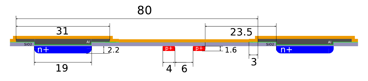
| Parameter | Value |
|---|---|
| Strip length | and |
| Strip width | |
| Strip pitch | |
| Metal overhang | |
| Number of strips | 256 and 64 |
| Overall dimensions | and |
| Coupling dielectric thickness | |
| Strip doping concentration (peak) | |
| Strip implant depth | |
| p-stop doping concentration (peak/ integrated) | / |
| p-stop depth | |
| p-spray doping concentration (peak/ integrated) | / |
| p-spray depth |
5 Materials, Thicknesses, and Production Technologies
Two important silicon wafer parameters that determine the evolution of full depletion voltage, signal, and noise with fluence are the active thickness and the oxygen content. The selected materials and thicknesses cover the relevant combination of parameters (Table 3), including the standard float-zone (FZ) material as a reference. In the current CMS strip tracker and thick float-zone sensors are used. All materials studied here have <100> crystal orientation.
| Active thickness () | |||
|---|---|---|---|
| Material | 300 | 200 | 120 |
| FZ | - | X | X |
| dd-FZ | X | X | X |
| MCz | - | X | - |
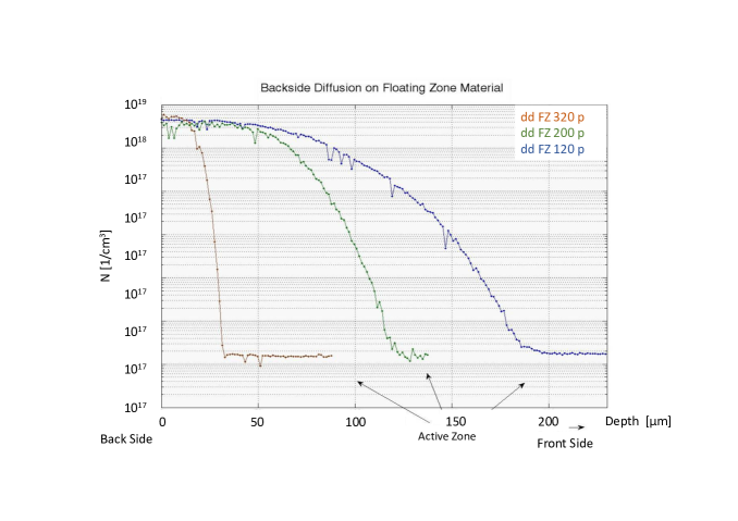
For the materials denoted with dd the active thickness is reduced by a special treatment provided by HPK (deep diffusion). The physical thickness of these wafers is always while the active thickness is reduced to the desired value by the diffusion of dopants from the backside. A doping profile for deep diffused p-type sensors obtained by Spreading Resistance Profiling (SRP) is shown in Fig. 5. Compared to direct-wafer bonded silicon, the deep diffusion process leads to a more gradual transition from the low resistivity back side to the high resistivity bulk.
This highly doped backside serves effectively as an ohmic contact to the remaining active region. The active thickness relevant for full depletion, electric field, and charge collection is thereby decoupled from the sensor thickness, which impacts mechanical stability and thermal performance. Moreover, for mechanical stability, very thin wafers need to be bonded to a carrier wafer during processing, an additional step that is not needed for the wafers treated with the deep diffusion process. The differences in the electrical properties of sensors produced using wafers processed with these two techniques are studied before and after irradiation. In addition, thick magnetic Czochralski (MCz) silicon sensors are studied. MCz has the advantage of a high oxygen concentration introduced during the crystal growth process in a quartz (SiO2) crucible.
The structures on all the selected materials were manufactured in three different processes: standard p-in-n, n-in-p with p-stop strip isolation, and n-in-p with p-spray strip isolation. In the current CMS strip tracker, p-in-n sensors are used. While initially both p-in-n and n-in-p options were considered for the upgraded CMS OT at the HL-LHC, the observation of non-Gaussian noise in p-in-n prototype sensors led to the decision to use n-in-p sensors [11]. Moreover, n-in-p sensors have the additional benefit that they always deplete from the readout side, which leads to good signal collection even for heavily irradiated sensors that are not fully depleted anymore. A drawback of n-in-p sensors is the need for p-stop or p-spray strip isolation to interrupt the electron inversion layer, which forms as a result of positive oxide charges.
The boron and phosphorus bulk doping concentrations are around cm-3 for the float-zone and 4– cm-3 for the MCz sensors . The doping concentration parameters measured by spreading resistance profiling (SRP) [12] are listed in Table 2. SRP is a technique used to measure resistivity as a function of depth in semiconductors.
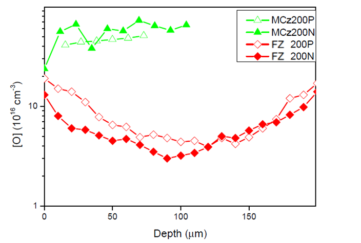
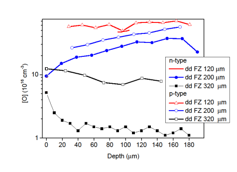
The oxygen concentration was measured using the secondary ion mass spectrometry (SIMS) technique, the results of which are shown in Figs. 6 and 7. The oxygen concentration ranges from cm-3 for the thick p-in-n float-zone material to cm-3 for the MCz material, and varies with depth. All materials studied (except for the n-type dd-FZ 320) are rather oxygen-rich compared to standard float-zone silicon, with typical oxygen concentrations in the range 0.5– cm-3. The reason for the relatively large difference in oxygen concentration between the thick deep diffused n and p type material is unknown. The oxygen concentration of the sensors in the current CMS OT is cm-3 (Fig. 7, right plot). These sensors have a deep diffused ohmic backside contact like in the dd-FZ 320 sensors studied in this paper.

6 Irradiation Campaign
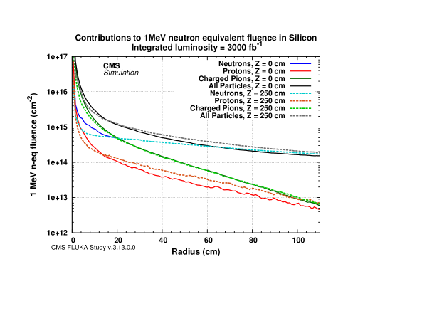
All structures were first electrically characterized, after which they were irradiated with reactor neutrons or proton beams to different fluences in several steps. After each irradiation step, the structures were annealed and again electrically characterized. The structures initially exposed to neutron irradiation later received a proton irradiation and vice versa, followed by another annealing treatment and electric characterization. This strategy allows us to investigate the properties of the materials after pure proton and neutron irradiation, and with mixed irradiation, using a minimum number of material samples. The fluence for charged and neutral hadrons at CMS, estimated with FLUKA simulations [13, 14] for an integrated luminosity of fb-1 at the HL-LHC, is shown in Fig. 8 as a function of the radial distance from the beam. Table 4 shows the fluence steps for neutron and proton irradiations corresponding to different radii of the OT of CMS as chosen for this study. The samples were irradiated with neutrons at the TRIGA Mark II reactor [15] at the Josef-Stefan-Institute in Ljubljana, Slovenia, corresponding to a 1 MeV equivalent hardness factor of 0.9 [16]. To study the dependence of radiation damage effects on the proton energy, several facilities were utilized for proton irradiation: the Karlsruhe Compact Cyclotron (KAZ) (23 MeV) [17] operated by the ZAG Zyklotron AG, the Proton Radiography Facility (pRad) at the Los Alamos LANSCE accelerator facility (800 MeV) [18], and the CERN Proton Synchrotron () [19], where the values represent the kinetic energy of the protons. In this paper results for samples irradiated with reactor neutrons and and protons are shown. The measured hardness factors are for and for protons [20].
| Radius [cm] | Proton [cm-2] | Neutron [cm-2] | Total [cm-2] | Active thickness |
|---|---|---|---|---|
| 40 | ||||
| 20 | ||||
| 15 | ||||
| 10 | ||||
| 5 |
After irradiation, the sensors were subjected to annealing in several steps as shown in Tab. 5. The annealing was done at , and at for the latter steps to avoid very long annealing times. The data shown in this paper are typically presented scaled to equivalent annealing times at a reference temperature of (room temperature) or . The scaling is based on a parametrization of the current related damage rate as a function of annealing time at different temperatures from Ref. [3]. For a given annealing time and temperature, an value is determined, and then the equivalent time at the reference temperature is obtained as the time leading to the same .
| Temperature | |||||||
| Annealing time | 20 min | 20 min | 40 min | 76 min | 15 min | 30 min | 60 min |
7 Measurement Techniques
7.1 Determination of Full Depletion Voltage and Leakage Current
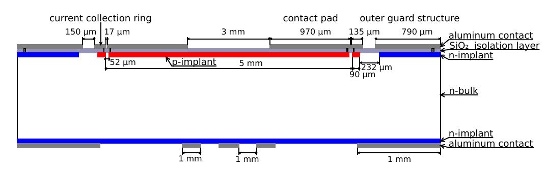
The test sensors (pad diodes and mini-strip sensors) are characterized in a current-voltage (-) and capacitance-voltage (-) measurement setup that allows the sensors to be cooled down to . A single guard ring surrounding the pad sensor is used to contain the electric field in the active volume to ensure high voltage stability and reduce the leakage current (Fig. 3). Unless stated otherwise, the guard ring of the pad sensor under test is grounded to ensure a well-defined sensitive volume. The strip sensors are surrounded by a bias ring, which is grounded during operation, and an outer guard ring, which is left floating. The humidity is reduced by a constant flow of dry air.
The full depletion voltage is extracted from - measurements, where the capacitance is evaluated in parallel mode. For non-irradiated sensors, the capacitance decreases with voltage and reaches a minimum (geometrical capacitance) when the sensor is fully depleted. For heavily irradiated sensors, the interpretation of the measurement results is more complicated. The measured capacitance strongly depends on the measurement temperature and frequency since irradiation-induced trap sites are filled and depleted by the AC voltage applied in the measurement. Whether a certain defect contributes depends on the characteristic time scale for filling and emitting in comparison with the inverse of the measurement frequency. The emission and capture probabilities for electrons and holes for each defect level are temperature dependent. Capacitance-voltage measurements were performed at at 1 kHz, and at at 1 kHz and 455 Hz. The full depletion voltage is determined from measurements at 1kHz and for measurements at 455 Hz. For the full depletion voltage the value is used at which the linear rise of versus voltage reaches an approximate plateau, by fitting straight lines to the data points below and above the kink, excluding the transition region, and determining their intersection. A low frequency like 455 Hz ensures that traps can dynamically be charged and discharged, given that emission timescales are in the millisecond-range at . If not stated otherwise, the full depletion voltage results for irradiated sensors shown in this paper are obtained from - measurements at and 455 Hz. As an alternative approach, recently, models with a position-dependent resistivity have been used to describe the frequency dependence of the parallel capacitance for irradiated sensors [22].
7.2 Measurements of Charge Collection for Diodes
The reduction of the collected charge due to trapping of charge carriers by radiation-induced defect levels in the silicon band gap is one of the main concerns for the HL-LHC tracker. The charge collection efficiency () at a certain bias voltage, , is defined as the fraction of the signal measured for an irradiated diode at compared to that of a non-irradiated diode of the same type measured at a reference voltage of . Charge carriers for this measurement can be generated either using an infrared laser or a source. While the latter provides a well-defined mean energy deposited in the silicon, the advantage of the laser is that the signal can be increased well above the noise level and the position of the laser light can be well controlled. Figure 9 shows the as a function of bias voltage for a non-irradiated and an irradiated diode, measured each with a laser and with a source (Strontium-90). It can be seen that the measurements agree rather well.
For the measurement with the laser, a transient current technique (TCT) setup [23] is used with an infrared laser with 1063 nm wavelength and a pulse width of (FWHM). The absorption length at this wavelength is of the order of , significantly larger than the typical thickness of a silicon sensor, which leads to an approximately uniform electron-hole pair creation as a function of depth, similar to the profile of a minimum ionizing particle. The resulting signal is amplified with a fast current preamplifier and recorded with a GHz bandwith digital oscilloscope. The charge collection efficiency is obtained by integrating the pulse over time and comparing the total charge (in arbitrary units) to the one obtained for a non-irradiated reference sensor at a reference voltage () that is above the full depletion voltage. A stability of the measured charge collection efficiency over time of better than can be reached in this kind of measurement. The uncertainty is dominated by the stability of the laser pulse. The intensity of the laser is set high enough to obtain a very good signal-to-noise ratio, but well below the onset of the "plasma effect" [24]. This was ensured by requiring the charge deposited by a single laser pulse to be less than 50 times that induced by a minimum ionizing particle. Moreover, the laser light is not focussed and has a spot size of about at the sensor surface. Fluctuations are further reduced by averaging signals over 512 events.
7.3 Measurement of Charge Collection for Strip Detectors with the ALIBAVA Setup
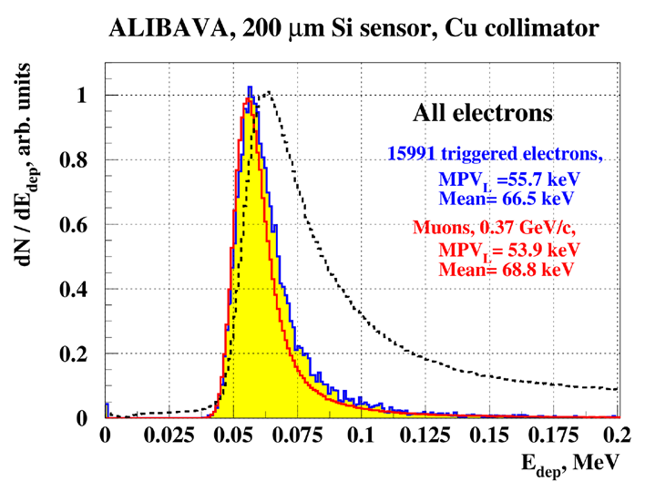
For the measurement of charge collection in strip sensors A Liverpool Barcelona Valencia (ALIBAVA) setup [25, 26] is used, based on the LHCb Beetle readout chip. Charge is generated using an infrared laser (wavelength ) or a source (Strontium-90). In the first case, a signal from the laser driver is used to trigger the readout of the data. In case of the source, a trigger based on one or two plastic scintillator planes on the side opposite to the source is used, thus imposing an energy cut on the electrons. With this energy cut, both shape and normalization of the distribution of electron-hole pairs generated by electrons in of silicon have been shown to be very similar to that of a minimum ionizing particle (Fig. 10) [27]. The settings of the pre-amplifier and shaper of the Beetle chip can be adjusted to obtain fast pulse shapes compatible with the 40 MHz clock of the LHC. However, when used with a source, which is non-synchronous with the Beetle clock, a longer pulse shape with a peak region of about 20 ns was used to ensure that a large fraction of the triggered events is useable for analysis. The peak region is defined as the part of the pulse which is within of the maximum pulse height. While the shaping time has an impact on the strip noise for irradiated sensors with substantial leakage current, charge collection measurements are less impacted.
7.4 Measurements of Strip Parameters with a Probe Station
This description was originally published in Ref. [11] and is repeated here for completeness. Initially, all sensors were electrically characterized with a probe station measuring the following quantities.
-
•
Total leakage current: The current in the bias line is measured versus bias voltage (-) with floating guard ring. The HPK sensors typically had current densities lower than .
-
•
Total capacitance: The capacitance of the sensor is measured versus bias voltage (-) with floating guard ring to extract the full depletion voltage.
-
•
Strip leakage currents: The leakage currents of individual strips are measured to check the uniformity.
-
•
Coupling capacitance: The capacitance between strip implant and metal strip is measured at 100 Hz and should be larger than 1.2 pFcm per m of implanted strip width.
-
•
Current through the dielectric: The current is measured between strip implant and metal strip applying 10 V and should be smaller than 1 nA.
-
•
Bias resistance: The bias resistor at each strip is evaluated by measuring the current when applying 2V to the DC pad. A resistance between 1 and is envisaged.
-
•
Interstrip capacitance: The capacitance between neighboring metal strips per unit strip length is measured at 1 MHz and should be below 1 pF/cm.
-
•
Interstrip resistance: The resistance between two strip implants is evaluated by measuring the - characteristic from to . It should be ten times higher than the bias resistance, and the resistivity should be larger than before irradiation.
8 Results
8.1 Leakage Current
One of the factors compromising the performance of a tracking detector over time is the increased sensor leakage current due to radiation damage. The consequences are increased electrical noise and power consumption, which increases the heat load and determines the temperature at which the sensors need to be operated to avoid thermal runaway. Thermal runaway describes a situation in which the cooling power is insufficient to cool the module, and the sensor temperature rises in a positive feedback loop, since the leakage current grows exponentially with temperature. The bias voltage, leakage current, and power consumed by the sensors impact the choice of power supplies and the design of the cooling system. On the other hand, technical limitations, such as maximum supply voltages or the lowest achievable sensor temperatures, may have an influence on the operating parameters and even the design of the sensors.
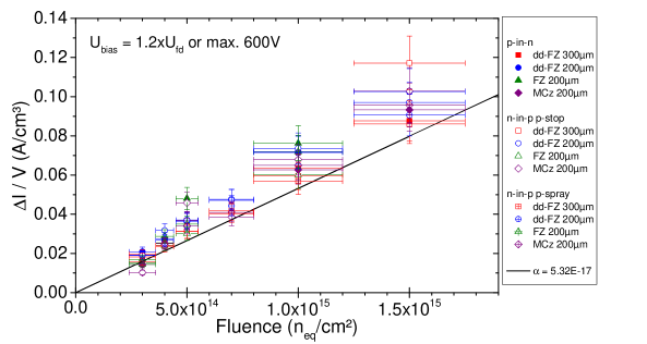
Figure 11 shows the volume generation current density as a function of particle fluence for diodes irradiated with or protons, neutrons, or a mix of protons and neutrons, respectively. To obtain reliable results, the currents, taken at 5 above the full depletion voltage, are plotted after annealing for 80 minutes at . The currents are measured at and scaled to by multiplying with a factor of 59 according to the procedure described in Ref. [28]. The leakage currents per volume are found to be proportional to the fluence, and they are in agreement with a proportionality factor Acm-1 found in previous measurements, as indicated in the plot. The measurements confirm that the leakage current universally scales with the NIEL, independent of silicon bulk material and irradiation type. In turn, the measurements of the leakage current can be used as a cross-check of the particle fluences obtained using dosimetry.
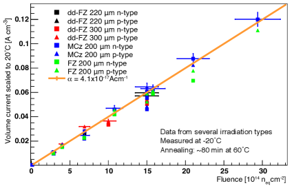
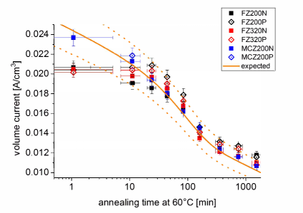
Figure 12 shows the development of the leakage current per volume as a function of annealing time at a temperature of for a variety of diodes irradiated with neutrons to cm-2. The leakage current is reduced by about a factor of two after annealing for 1000 minutes at and follows the Hamburg model [1].
The current measured for strip sensors 20222For strip sensors, a voltage 20 above the nominal full depletion voltage was chosen to ensure that the sensors are fully depleted. While the change in the volume current above full depletion is very small, an underdepleted sensor would draw less current. above the full depletion voltage after annealing for 10 minutes at is shown in Fig. 13. For comparison, the straight line describes the volume current as a function of fluence for diodes with this annealing time ( A cm-1). While again a linear dependence on fluence is observed, most sensors display a larger current compared to diodes, likely the result of an additional surface current component.
8.2 Full Depletion Voltage
In this section, systematic studies of the full depletion voltage after irradiation and annealing are presented. The dependence of the full depletion voltage on particle fluence and type ( and protons, neutrons) is studied for samples with different silicon crystals, polarity, and thickness.
Figure 14 shows the full depletion voltage and the average effective space charge concentration () for thick float-zone diodes as a function of 1 MeV neutron equivalent fluence for proton irradiation and proton plus additional neutron irradiation ("mixed irradiation"). The effective space charge concentration is related to the full depletion voltage by
where is the thickness of the active volume of the device.
It should be stressed that the concept of an effective space charge concentration constant over the thickness of the sensor derived from the full depletion voltage obtained by - measurements has been shown to be inadequate for irradiated sensors in the fluence range studied in this paper ( cm-2 ). Irradiated sensors can be better described by a double junction model, which leads to a double peaked electric field [4, 29]. In this paper, the full depletion voltage is merely used as a figure of merit to compare the behavior of different sensors after irradiation and annealing, without the same straightforward meaning as for non-irradiated sensors.
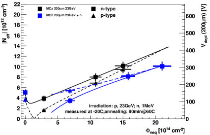
The dependence of the full depletion voltage on fluence for the p-in-n float-zone diodes after mixed irradiation is similar to that after proton irradiation only. In general, the fact that p bulk material does not undergo space charge sign inversion leads to higher depletion voltages compared to n-type. For n-in-p devices, the full depletion voltages after mixed irradiation are above the ones for proton irradiation only. A very large increase in depletion voltage after additional neutron irradiation is visible especially at small fluences. In this study, the impact of the additional neutron irradiation is larger at smaller fluences as these correspond to larger radii in the tracker, which in turn implies a larger neutron fraction (Table 4). While the cause of this increase might be linked to acceptors created after neutron irradiation, no attempts were made to understand the effect quantitatively.
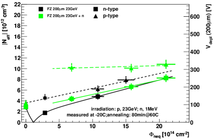
Figure 15 shows the full depletion voltage and effective space charge concentration for thick magnetic Czochralski diodes as a function of 1 MeV neutron equivalent fluence for proton irradiation and mixed irradiation. In this case, the full depletion voltages for p-in-n diodes after mixed irradiation lie systematically below the curves after proton irradiation only. This can be attributed to donors being created in oxygen rich magnetic Czochralski silicon during GeV proton irradiation, compensating the effect of neutron irradiation-induced acceptors. These findings confirm that NIEL scaling is violated with respect to the full depletion voltage. The effects of neutron and GeV proton irradiation partially cancel each other in oxygen rich n-type material, confirming previous observations [30].
The differences between float-zone and magnetic Czochralski sensors after mixed irradiation ( protons plus 1 MeV neutrons) are especially visible in the capacitance-voltage curves. In Fig. 16, the measured inverse capacitance squared () is plotted as a function of applied voltage for 200 m thick n-in-p float-zone and magnetic Czochralski mini strip sensors irradiated to cm-2 for different annealing times, scaled to room temperature. While the curves lie virtually on top of each other for the magnetic Czochralski sensor, a large variation in capacitance below depletion is visible for the float-zone sensor.
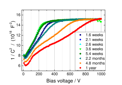
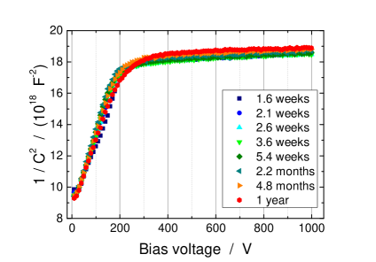
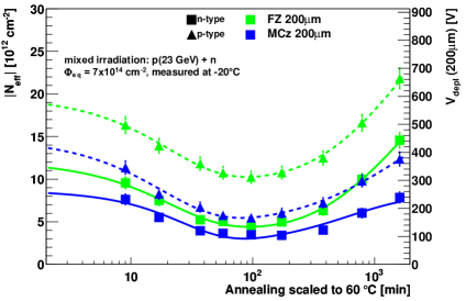
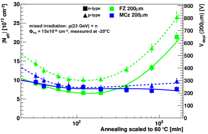
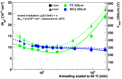
Figure 17 shows the development of the full depletion voltage and effective space charge concentration extracted from - measurements with annealing time after proton plus 1 MeV neutron irradiation for 7, 15 and cm-2, respectively, for float-zone and magnetic Czochralski diodes. The annealing time is scaled to +. An annealing time of 1000 minutes at + corresponds to 272 days at room temperature (+), based on the temperature dependence of the annealing of the leakage current described in Sec. 6. The data points are fitted with the Hamburg model [1], the fit parameters can be found in the appendix of Ref. [27]. The full depletion voltages of the n-in-p and p-in-n float-zone sensors show the well-known behavior: an initial drop (short term annealing) to a minimum (stable damage), followed by a rise (reverse or long-term annealing). For the magnetic Czochralski diodes, on the other hand, a very stable full depletion voltage as a function of annealing time can be observed, especially for the two larger fluences. An advantage of the magnetic Czochralski material is that it would be less important to keep the tracking detectors cold during maintenance periods to avoid reverse annealing. Moreover, by intentionally subjecting the sensors to some annealing, the leakage current can be reduced.
8.3 Charge Collection
The hit reconstruction efficiency of the future CMS tracker depends on the collected charge and the electronic noise of each readout channel. For reliable tracker operation, a sufficiently large signal that is as stable as possible over the operation time is therefore required. For a given sensor, the collected charge depends on the fluence it was subjected to, the annealing state, and the applied voltage. The goal of this measurement is to study charge collection as a function of these parameters and to find a combination of sensor material and thickness of the active silicon layer that is suited for sensors for the CMS tracker at the HL-LHC. To study silicon bulk material effects, charge collection is first measured with pad diodes using infrared laser measurements. The study is then extended to strip sensors for which the details of the charge collection can be different owing to the weighting field and differences in the electric fields. The weighting field is a measure of the electrostatic coupling between the moving charge and the sensing electrode and has units of .
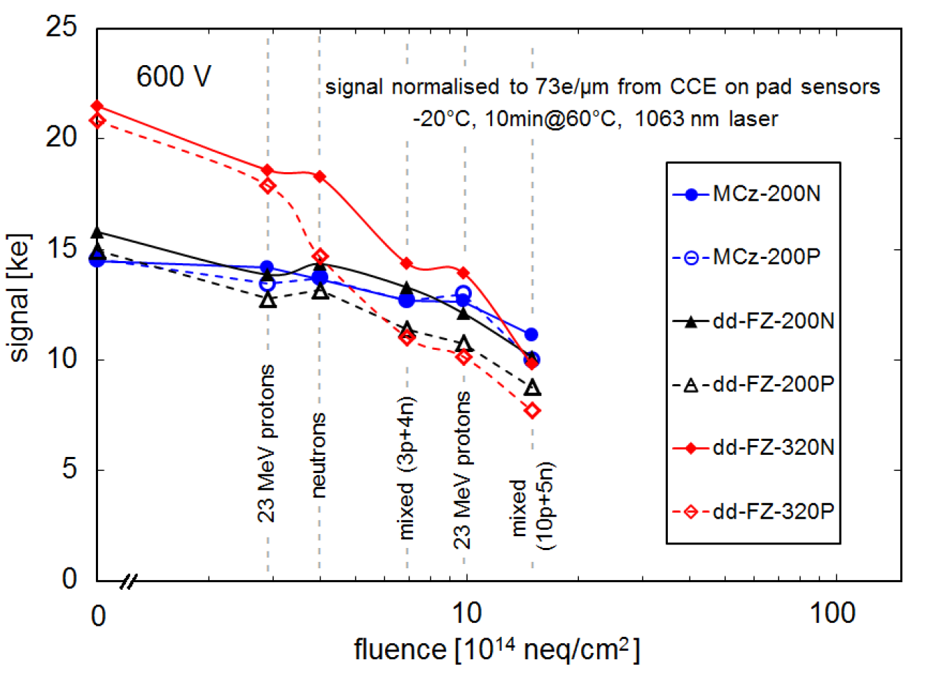
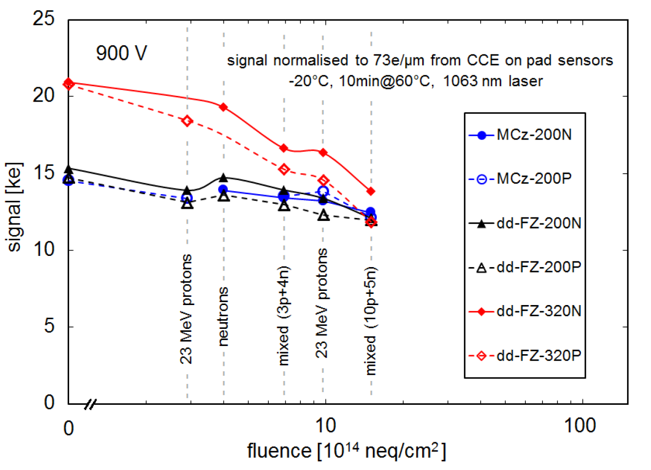
First, the collected charge is compared for 200 and thick pad diodes. Figure 18 shows the collected charge after irradiation with protons and neutrons measured at nd , respectively. The possibility to increase the sensor bias voltage from the nominal o is foreseen for the CMS OT at the HL-LHC to obtain larger signals [6]. The charge collection efficiency is first measured relative to a non-irradiated reference diode using an infrared laser and scaled to units of collected charge by a factor of 73 electrons per active bulk silicon; this factor applies to the most probable value of the Landau distribution. At lower fluences, more charge is collected in thick silicon than in silicon. However, for a bias voltage of , the collected charge for the thicker sensors drops rapidly as a function of fluence, especially for the n-in-p deep diffused float-zone diode, which has been shown to have a full depletion voltage which rises quickly with fluence. At , more charge is collected by the silicon for all fluences shown.
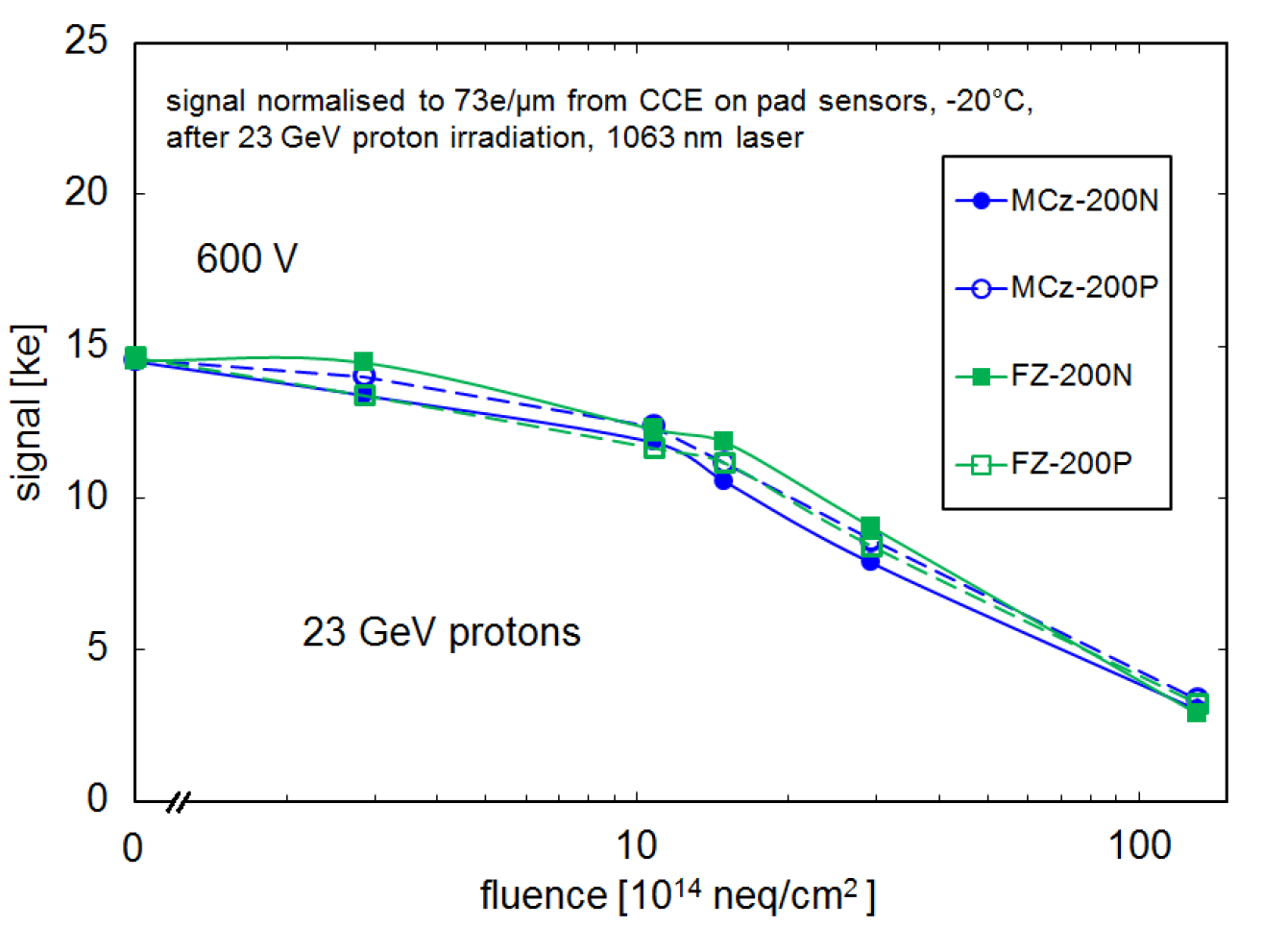
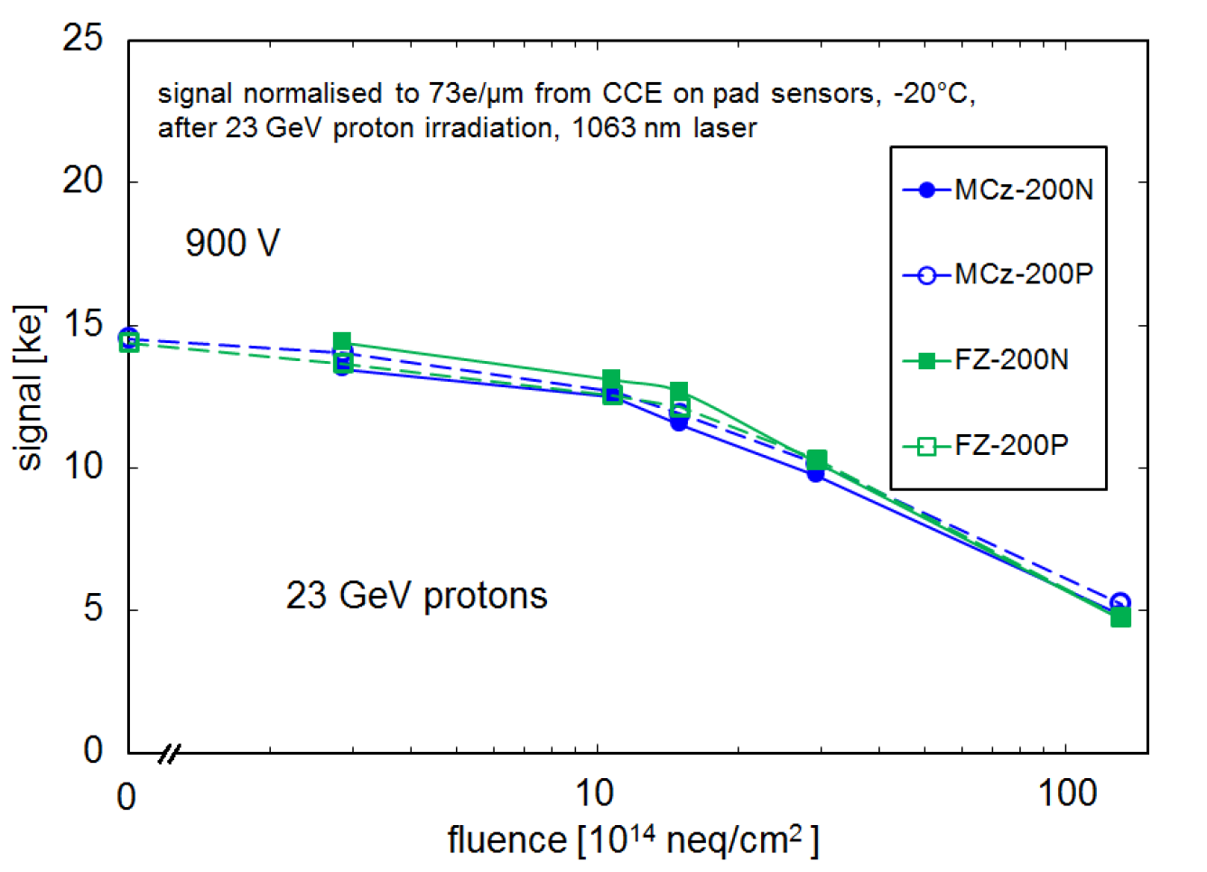
Next, the collected charge is compared for thick pad diodes for different polarities (n-in-p and p-in-n) and bulk materials (FZ and MCz) after irradiation with protons. The charge collection was again measured at nd (Fig. 19). While at large fluences more signal is collected at bias voltage, very little variation with material and polarity is observed.
All readout chips for the CMS OT at the HL-LHC will feature binary readout [6], meaning that strips with signals above a threshold are marked and only the strip addresses are read out. The relevant quantity to study is therefore the pulse height of the strip with the largest pulse height in a cluster of adjacent strips (“seed charge”) rather than the total cluster charge.
The expected noise for the CMS Binary Chip (CBC) [31] used in 2S modules in the outer layers of the OT is of the order of 1000 electrons. Requiring a threshold of four times the noise, and an MPV of the seed strip three times higher than the threshold leads to a required MPV of 12000 electrons. For the PS modules in the inner OT layers, the expected noise for the Short Strip ASIC (SSA) is around 800 electrons [32], leading to a required threshold of 3200 electrons and a minimum seed signal (MPV) of 9600 electrons.
For the following charge collection plots, the ALIBAVA system with a source (Strontium-90) was used. In Fig. 20 the MPV of the charge recorded by the seed strip is shown as a function of particle fluence for 200 m thick float-zone sensors. On a log-log scale, the reduction of signal is roughly linear with fluence, consistent with a power law. The nominal fluences for an integrated luminosity of are about cm-2 and cm-2 for the innermost 2S and PS sensors, respectively. For PS as well as 2S sensor modules, the signal for a thick sensor biased to would be around or below the required minimum at the highest expected fluence.
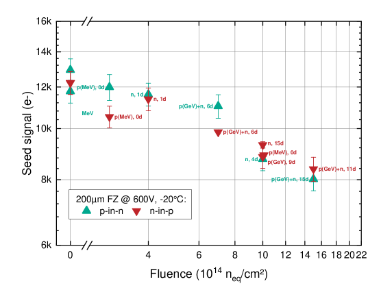
Figure 21 shows the MPV of the charge recorded by the seed strip for 200 and thick float-zone and magnetic Czochralski strip sensors as a function of the equivalent annealing time at room temperature after mixed proton and neutron irradiation to fluences of and cm-2, respectively. These fluences correspond to tracker layer radii of and and an integrated luminosity of . The sensors were biased to . The collected charge for the float-zone sensors varies with annealing time, displaying maxima at several hundred hours equivalent annealing time at room temperature and a decrease thereafter. The decrease is most pronounced at the larger fluence and for the thick sensors owing to under-depletion of the sensors. For the thicker float-zone p-in-n sensor, a very strong decrease of the seed signal with annealing can already be observed at cm-2, whereas reliable measurements at cm-2 were not possible owing to non-Gaussian noise. The strong dependence of the full depletion voltage on annealing time of the float-zone sensors has already been shown in Fig. 16. The magnetic Czochralski sensors, on the other hand, show a very constant charge collection as a function of annealing time (see also Sec. 8.2). These findings illustrate again that bias voltages beyond are needed for optimal charge collection for fluences in the range cm-2.
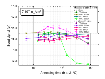
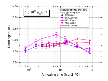
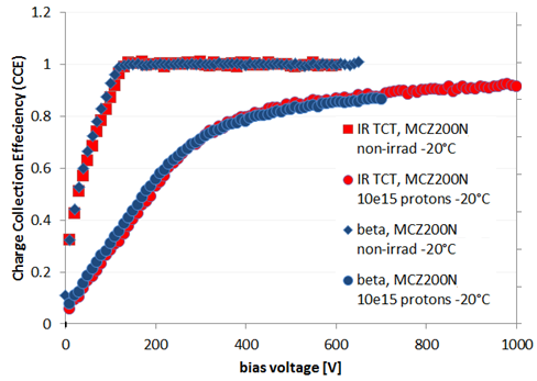
Figure 22 shows the MPV of the charge recorded by the seed strip as a function of applied bias voltage for a fluence of cm-2 for n-in-p float-zone and magnetic Czochralski strip sensors. The annealing corresponds to 3300 hours at room temperature.
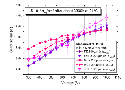
For voltages up to around 700 V, the seed signal of the thick sensor is not higher than that of the sensors. At higher voltages, thicker silicon leads to additional collected charge under these conditions. At voltages up to around 700 V, the magnetic Czochralski sensor shows an increased charge collection compared to float-zone silicon of the same thickness, consistent with the findings described above. At larger voltages, this difference disappears. This again points to the fact that differences in charge collection between materials are due to variations in full depletion voltage and electric field. At very large bias voltages, these differences are small and the reduction in charge collection after irradiation and annealing is dominated by trapping, which is assumed to be independent of the material. The measurements described in this section indicate that thick sensors would be preferable for the use in the CMS OT with the option to operate them at voltages of up to .
8.4 Measurements of Individual Strip Parameters
This section summarizes measurements of strip parameters using probe stations. Details of these measurements and the setups used can be found in Ref. [33].
The measurements have been performed at + before irradiation and at after irradiation, after about 10 minutes annealing at + and at a bias voltage of . The measurement results as a function of fluence are shown in Figs. 23 – 26.
Except for the interstrip resistance, the measured strip parameters do not show any significant change after irradiations up to cm-2.
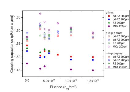
The coupling capacitance is shown in Fig. 23. A slightly higher coupling capacitance was observed in n-in-p sensors. Looking closely, one can observe a small () increase of the coupling capacitance for n-in-p sensors and a small decrease for p-in-n sensors with increasing fluence. The origin is still unknown, but this effect is very small and does not affect the performance of the sensor at all. The coupling capacitance is specified to be above per m of implanted strip width.
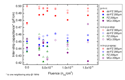
Figure 24 shows the measurement of the interstrip capacitance. The thicker sensors with lower backplane capacitance show higher interstrip capacitance. The measurement accuracy of the interstrip capacitance is around and within this error no change of this parameter can be observed with increasing fluence. Therefore we do not expect an increasing contribution to the readout noise from the interstrip capacitance, which is specified to be below .
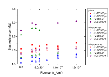
Figure 25 shows a step of the measured polysilicon resistance from non-irradiated to the first irradiated samples, which is due to the different temperatures used. The bias resistance increases by about with decreasing temperature [33]. The irradiations did not affect the resistance of the polysilicon resistors. Bias resistances between nd are acceptable as long as the uniformity across the sensor is good.
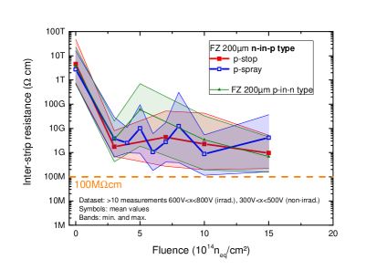
The measured interstrip resistance333The interstrip resistance scales linearly with the inverse of the strip length and the given value has to be divided by the strip length. has been significantly affected by irradiation (Fig. 26). It has dropped from a large value above 1 T to a measured minimal value of 100 M after an irradiation of cm-2. No significant difference of p-stop or p-spray isolation is observed for the applied process. For a final strip length of 2.5 cm this would result in an interstrip resistance of 40 M, which is still much larger than the bias resistance of about 2 M. The measurement is performed by recording the strip leakage current while applying a small additional potential ( to ) resulting in an - curve between two strips. The resistance is the inverse of the slope, which can be quite flat on top of a huge leakage current offset. The accuracy of this method is not very high and for large currents one can only extract lower limits.
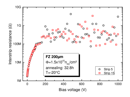
An example is shown in Fig. 27. At low bias voltages, for which the interstrip resistance is still low, the spread of the measurements is small. For higher resistances the spread increases strongly and the measurements can only reflect the noise; the actual interstrip resistance can be (much) higher. The values in Fig. 26 are therefore the mean of measurement values between nd ; the bands reflect the minimum and maximum values. However, the measured interstrip resistance at larger bias voltages is always well above the bias resistance, as required for good charge separation for individual strips.
9 Summary
CMS has executed a measurement and irradiation campaign to compare silicon sensor materials and design choices for Outer Tracker (OT) sensors for the high-luminosity phase of the LHC with the aim to provide input for the decision process. A number of segmented detectors, special purpose test structures, and pad diodes were implemented by a single producer on a variety of wafers. In this paper we have presented results of measurements of pad diodes and strip sensors. Results on the leakage current, the full depletion voltage and the charge collection efficiency have been shown before and after irradiation with reactor neutrons, and protons of different energies. The full depletion voltage for irradiated sensors is simply used as a figure of merit for comparison without the same straightforward meaning as for non-irradiated sensors.
Three silicon sensor materials were studied in detail: magnetic Czochralski, float-zone, and float-zone silicon in which the active thickness was reduced by deep diffusion of dopants from the backside. The oxygen-rich thick magnetic Czochralski sensors have shown a particularly stable full depletion voltage and charge collection with annealing. A partial compensation of the effects of irradiation with neutrons and GeV protons on the full depletion voltage was observed in n-type magnetic Czochralski material. As long as the applied voltage is large enough for a given fluence, the differences in charge collection are small, and all of these materials are suitable choices.
The leakage current measured in strip sensors was significantly higher than that measured in diodes, likely due to additional surface currents. This has to be taken into account in estimates of the sensor module power consumption and cooling needs, and the noise when designing the CMS tracker. While individual strip parameters change with irradiation, the changes for the fluences studied have been shown to be in a range which has little impact on sensor performance. The interstrip isolation has been studied up to an equivalent fluence of cm-2 and was found to be sufficient for all sensor types included in this study.
CMS decided in 2013 to use n-in-p sensors for the OT [11, 6]. In addition to the well known advantage of n-in-p sensors of depleting from the segmented side, irradiated p-in-n prototype sensors showed strong non-Gaussian noise [11].
Detailed charge collection studies on diodes and mini strip sensors show that for the entire CMS OT with equivalent fluences up to cm-2, sensors with a thickness in the order of are best suited. They require operation voltages of up to 800 V at the end of the HL-LHC running period.
Acknowledgment
The tracker groups gratefully acknowledge financial support from the following funding agencies: BMWFW and FWF (Austria); FNRS and FWO (Belgium); CERN; MSE and CSF (Croatia); Academy of Finland, MEC, and HIP (Finland); CEA and CNRS/IN2P3 (France); BMBF, DFG, and HGF (Germany); GSRT (Greece); NKFIA K124850, and Bolyai Fellowship of the Hungarian Academy of Sciences (Hungary); DAE and DST (India); IPM (Iran); INFN (Italy); PAEC (Pakistan); SEIDI, CPAN, PCTI and FEDER (Spain); Swiss Funding Agencies (Switzerland); MST (Taipei); STFC (United Kingdom); DOE and NSF (U.S.A.).
Individuals have received support from HFRI (Greece).
The research leading to these results has received funding from the
European Commission under the FP7 Research Infrastructures project AIDA,
grant agreement no. 262025.
References
- [1] The RD48 Collaboration, Radiation Hard Silicon Detectors - Developments by the RD48 (ROSE) Collaboration, Nucl. Instr. and Meth. A 466 (2001) 308 (NIMA electronic version).
- [2] The RD50 Collaboration, RD50 Status Report 2008, CERN-LHCC-2010-012, 2010.
- [3] M. Moll, Radiation Damage in Silicon Particle Detectors - Microscopic Defects and Macroscopic Properties, PhD thesis, Hamburg University, DESY-THESIS-1999-040 (1999).
- [4] V. Eremin, E. Verbitskaya, Z. Li, The origin of double peak electric field distribution in heavily irradiated silicon detectors, Nucl. Instr. and Meth. A 476 (2002) 556-564.
- [5] B. Schmidt, The High-Luminosity upgrade of the LHC: Physics and Technology Challenges for the Accelerator and the Experiments, J. Phys.: Conf. Ser. 706 (2016) 022002.
- [6] CMS Collaboration, The Phase-2 Upgrade of the CMS Tracker, CERN-LHCC-2017-09, CMS-TDR-014 (2017).
- [7] G. Lindström, M. Moll, E. Fretwurst, Radiation hardness of silicon detectors - a challenge from high-energy physics, Nucl. Instr. and Meth. A 426 (1999) 1-15.
- [8] G.Lindström, M. Moll, E. Fretwurst, Radiation damage in silicon detectors, Nucl. Instr. and Meth. A 512 (2003) 30-43.
- [9] http://www.hamamatsu.com
- [10] CMS Collaboration, The CMS Experiment at the CERN LHC, JINST 3 (2008), S08004.
- [11] The CMS Tracker Group of the CMS Collaboration, P-Type Silicon Strip Sensors for the new CMS Tracker at HL-LHC, 2017 JINST 12 P06018.
- [12] W. Treberspurg, T. Bergauer, M. Dragicevic, J. Hrubec, M. Krammer, and M. Valentan, Measuring doping profiles of silicon detectors with a custom-designed probe station, 2012 JINST 7 P11009.
- [13] A. Ferrari, P. R. Sala, A. Fassò and J. Ranft, FLUKA: a multi-particle transport code, CERN-2005-10, INFN/TC 05/11, SLAC-R-773 (2005).
- [14] T. T. Böhlen, F. Cerutti, M. P. W. Chin, A. Fassò, A. Ferrari, P. G. Ortega, A. Mairani, P. R. Sala, G. Smirnov and V. Vlachoudis, The FLUKA Code: Developments and Challenges for High Energy and Medical Applications, Nuclear Data Sheets 120 (2014) 211, doi:http://dx.doi.org/10.1016/j.nds.2014.07.049
- [15] L. Snoj, G. Žerovnik, A.Trkov, Computational analysis of irradiation facilities at the JSI TRIGA reactor, Applied Radiation and Isotopes, 70 (2012) 483. doi:10.1016/j.apradiso.2011.11.042.
- [16] G. Kramberger, Signal development in irradiated silicon detectors , PhD thesis, University of Ljubljana (2001).
- [17] https://www.ekp.kit.edu/english/irradiation_center.php
- [18] http://lansce.lanl.gov/facilities/pRad/index.php
- [19] https://ps-irrad.web.cern.ch
- [20] P. Allport et al., Experimental Determination of Proton Hardness Factors at Several Irradiation Facilities, arXiv:1908.03049 [physics.ins-det].
- [21] CMS Collaboration, 1-D plot covering CMS tracker, showing FLUKA simulated 1MeV neutron equivalent in Silicon including contributions from various particle types, CMS-DP-2015-022.
- [22] R. Klanner and J. Schwandt, On the weighting field and admittance of irradiated Si-sensors, arXiv:1911.12633 [physics.ins-det].
- [23] G. Kramberger, Advanced Transient Current Technique Systems, PoS (Vertex2014) 032, doi:10.22323/1.227.0032.
- [24] J. Becker, D. Eckstein, R. Klanner, G. Steinbrück, Impact of plasma effects on the performance of silicon sensors at an X-ray FEL, Nucl. Instr. and Meth. A 615 (2010) 230.
- [25] http://www.alibavasystems.com
- [26] R. Marco-Hernández on behalf of the ALIBAVA Collaboration, A portable readout system for silicon microstrip sensors, Nucl. Instr. and Meth. A 623 (2010) 207-209.
- [27] J. Erfle, Irradiation Study of Different Silicon Materials for the CMS Tracker Upgrade, PhD thesis, Hamburg University, 2014.
- [28] A. Chilingarov, Generation current temperature scaling, RD50 technical note, http://rd50.web.cern.ch/RD50/doc/Internal/rd50_2011_001-I-T_scaling.pdf
- [29] V. Chiochia et al., A double junction model of irradiated silicon pixel sensors for LHC, Nucl. Instr. and Meth. A 568 (2006) 51-55.
- [30] G. Kramberger et al., Performance of silicon pad detectors after mixed irradiations with neutrons and fast charged hadrons, Nucl. Instr. and Meth. A 609 (2009) 142.
- [31] G. Hall et al., CBC2: A CMS microstrip readout ASIC with logic for track-trigger modules at HL-LHC, Nucl. Instr. and Meth. A 765 (2014) 214. doi:10.1016/j.nima.2014.04.056.
- [32] A. Caratelli et al., Short Strip ASIC Specifications Document, September 2016, https://espace.cern.ch/CMS-MPA/SitePages/Documents.aspx
- [33] K.-H. Hoffmann, Development of new Sensor Designs and Investigations on Radiation Hard Silicon Strip Sensors for the CMS Tracker Upgrade at the High Luminosity Large Hadron Collider, PhD thesis, Karlsruhe Institute of Technology, IEKP-KA/2013-1 (2013), http://ekp-invenio.physik.uni-karlsruhe.de/record/48272/files/iekp-ka2013-1.pdf
Tracker Group of the CMS Collaboration
Institut für Hochenergiephysik, Wien, Austria
W. Adam, T. Bergauer, D. Blöch, E. Brondolin1, M. Dragicevic, R. Frühwirth2, V. Hinger, H. Steininger, W. Treberer-Treberspurg
Universiteit Antwerpen, Antwerpen, Belgium
W. Beaumont, D. Di Croce, X. Janssen, J. Lauwers, P. Van Mechelen, N. Van Remortel
Vrije Universiteit Brussel, Brussel, Belgium
F. Blekman, S.S. Chhibra, J. De Clercq, J. D’Hondt, S. Lowette, I. Marchesini, S. Moortgat, Q. Python, K. Skovpen, E. Sørensen Bols, P. Van Mulders
Université Libre de Bruxelles, Bruxelles, Belgium
Y. Allard, D. Beghin, B. Bilin, H. Brun, B. Clerbaux, G. De Lentdecker, H. Delannoy, W. Deng, L. Favart, R. Goldouzian, A. Grebenyuk, A. Kalsi, I. Makarenko, L. Moureaux, A. Popov, N. Postiau, F. Robert, Z. Song, L. Thomas, P. Vanlaer, D. Vannerom, Q. Wang, H. Wang, Y. Yang
Université Catholique de Louvain, Louvain-la-Neuve, Belgium
O. Bondu, G. Bruno, C. Caputo, P. David, C. Delaere, M. Delcourt, A. Giammanco, G. Krintiras, V. Lemaitre, A. Magitteri, K. Piotrzkowski, A. Saggio, N. Szilasi, M. Vidal Marono, P. Vischia, J. Zobec
Institut Ruđer Bošković, Zagreb, Croatia
V. Brigljević, S. Ceci, D. Ferenček, M. Roguljić, A. Starodumov3, T. Šuša
Department of Physics, University of Helsinki, Helsinki, Finland
P. Eerola, J. Heikkilä
Helsinki Institute of Physics, Helsinki, Finland
E. Brücken, T. Lampén, P. Luukka, L. Martikainen, E. Tuominen
Lappeenranta University of Technology, Lappeenranta, Finland
T. Tuuva
Université de Strasbourg, CNRS, IPHC UMR 7178, Strasbourg, France
J.-L. Agram4, J. Andrea, D. Bloch, C. Bonnin, G. Bourgatte, J.-M. Brom, E. Chabert, L. Charles, E. Dangelser, D. Gelé, U. Goerlach, L. Gross, M. Krauth, N. Tonon
Université de Lyon, Université Claude Bernard Lyon 1, CNRS-IN2P3, Institut de Physique Nucléaire de Lyon, Villeurbanne, France
G. Baulieu, G. Boudoul, L. Caponetto, N. Chanon, D. Contardo, P. Dené, T. Dupasquier, G. Galbit, N. Lumb, L. Mirabito, B. Nodari, S. Perries, M. Vander Donckt, S. Viret
RWTH Aachen University, I. Physikalisches Institut, Aachen, Germany
C. Autermann, S. Böhm, L. Feld, W. Karpinski, M.K. Kiesel, K. Klein, M. Lipinski, D. Meuser, A. Pauls, G. Pierschel, M. Preuten, M. Rauch, N. Röwert, J. Schulz, M. Teroerde, J. Wehner, M. Wlochal
RWTH Aachen University, III. Physikalisches Institut B, Aachen, Germany
C. Dziwok, G. Fluegge, T. Müller, O. Pooth, A. Stahl, T. Ziemons
Deutsches Elektronen-Synchrotron, Hamburg, Germany
M. Aldaya, C. Asawatangtrakuldee, G. Eckerlin, D. Eckstein, T. Eichhorn, E. Gallo, M. Guthoff, M. Haranko, A. Harb, J. Keaveney, C. Kleinwort, R. Mankel, H. Maser, M. Meyer, M. Missiroli, C. Muhl, A. Mussgiller, D. Pitzl, O. Reichelt, M. Savitskyi, P. Schuetze, R. Stever, R. Walsh, A. Zuber
University of Hamburg, Hamburg, Germany
A. Benecke, H. Biskop, P. Buhmann, M. Centis-Vignali, A. Ebrahimi, M. Eich, J. Erfle, F. Feindt, A. Froehlich, E. Garutti, P. Gunnellini, J. Haller, A. Hinzmann, A. Junkes, G. Kasieczka, R. Klanner, V. Kutzner, T. Lange, M. Matysek, M. Mrowietz, C. Niemeyer, Y. Nissan, K. Pena, A. Perieanu, T. Poehlsen, O. Rieger, C. Scharf, P. Schleper, J. Schwandt, D. Schwarz, J. Sonneveld, G. Steinbrück, A. Tews, B. Vormwald, J. Wellhausen, I. Zoi
Institut für Experimentelle Teilchenphysik, KIT, Karlsruhe, Germany
M. Abbas, L. Ardila, M. Balzer, C. Barth, T. Barvich, M. Baselga, T. Blank, F. Bögelspacher, E. Butz, M. Caselle, W. De Boer, A. Dierlamm, R. Eber, K. El Morabit, J.-O. Gosewisch, F. Hartmann, K.-H. Hoffmann, U. Husemann, R. Koppenhöfer, S. Kudella, S. Maier, S. Mallows, M. Metzler, Th. Muller, M. Neufeld, A. Nürnberg, M. Printz, O. Sander, D. Schell, M. Schröder, T. Schuh, I. Shvetsov, H.-J. Simonis, P. Steck, M. Wassmer, M. Weber, A. Weddigen
Institute of Nuclear and Particle Physics (INPP), NCSR Demokritos, Aghia Paraskevi, Greece
G. Anagnostou, P. Asenov, P. Assiouras, G. Daskalakis, A. Kyriakis, D. Loukas, L. Paspalaki
Wigner Research Centre for Physics, Budapest, Hungary
T. Balázs, F. Siklér, T. Vámi, V. Veszprémi
University of Delhi, Delhi, India
A. Bhardwaj, C. Jain, G. Jain, K. Ranjan
Saha Institute of Nuclear Physics, Kolkata, India
R. Bhattacharya, S. Dutta, S. Roy Chowdhury, G. Saha, S. Sarkar
INFN Sezione di Baria, Università di Barib, Politecnico di Baric, Bari, Italy
P. Cariolaa, D. Creanzaa,c, M. de Palmaa,b, G. De Robertisa, L. Fiorea, M. Incea,b, F. Loddoa, G. Maggia,c, S. Martiradonnaa, M. Mongellia, S. Mya,b, G. Selvaggia,b, L. Silvestrisa
INFN Sezione di Cataniaa, Università di Cataniab, Catania, Italy
S. Albergoa,b, S. Costaa,b, A. Di Mattiaa, R. Potenzaa,b, M.A. Saizua,5, A. Tricomia,b, C. Tuvea,b
INFN Sezione di Firenzea, Università di Firenzeb, Firenze, Italy
G. Barbaglia, M. Brianzia, A. Cassesea, R. Ceccarellia,b, R. Ciaranfia, V. Ciullia,b, C. Civininia, R. D’Alessandroa,b, E. Focardia,b, G. Latinoa,b, P. Lenzia,b, M. Meschinia, S. Paolettia, L. Russoa,b, E. Scarlinia,b, G. Sguazzonia, L. Viliania,b
INFN Sezione di Genovaa, Università di Genovab, Genova, Italy
S. Cerchia, F. Ferroa, R. Mulargiaa,b, E. Robuttia
INFN Sezione di Milano-Bicoccaa, Università di Milano-Bicoccab, Milano, Italy
F. Brivioa,b, M.E. Dinardoa,b, P. Dinia, S. Gennaia, L. Guzzi, S. Malvezzia, D. Menascea, L. Moronia, D. Pedrinia, D. Zuoloa,b
INFN Sezione di Padovaa, Università di Padovab, Padova, Italy
P. Azzia, N. Bacchettaa, D. Biselloa, T.Dorigoa, N. Pozzobona,b, M. Tosia,b
INFN Sezione di Paviaa, Università di Bergamob, Bergamo, Italy
F. De Canioa,b, L. Gaionia,b, M. Manghisonia,b, L. Rattia, V. Rea,b, E. Riceputia,b, G. Traversia,b
INFN Sezione di Perugiaa, Università di Perugiab, CNR-IOM Perugiac, Perugia, Italy
G. Baldinellia,b, F. Bianchia,b, M. Biasinia,b, G.M. Bileia, S. Bizzagliaa, M. Capraia, B. Checcuccia, D. Ciangottinia, L. Fanòa,b, L. Farnesinia, M. Ionicaa, R. Leonardia,b, G. Mantovania,b, V. Mariania,b, M. Menichellia, A. Morozzia, F. Moscatellia,c, D. Passeria,b, P. Placidia,b, A. Rossia,b, A. Santocchiaa,b, D. Spigaa, L. Storchia, C. Turrionia,b
INFN Sezione di Pisaa, Università di Pisab, Scuola Normale Superiore di Pisac, Pisa, Italy
K. Androsova, P. Azzurria, G. Bagliesia, A. Bastia, R. Beccherlea, V. Bertacchia,c, L. Bianchinia, T. Boccalia, L. Borrelloa, F. Bosia, R. Castaldia, M.A. Cioccia,b, R. Dell’Orsoa, G. Fedia, F. Fioria,c, L. Gianninia,c, A. Giassia, M.T. Grippoa,b, F. Ligabuea,c, G. Magazzua, E. Mancaa,c, G. Mandorlia,c, E. Mazzonia, A. Messineoa,b, A. Moggia, F. Morsania, F. Pallaa, F. Palmonaria, F. Raffaellia, A. Rizzia,b, P. Spagnoloa, R. Tenchinia, G. Tonellia,b, A. Venturia, P.G. Verdinia
INFN Sezione di Torinoa,Università di Torinob, Politecnico di Torinoc, Torino, Italy
R. Bellana,b, M. Costaa,b, R. Covarellia,b, G. Dellacasaa, N. Demariaa, A. Di Salvoa,c, G. Mazzaa, E. Migliorea,b, E. Monteila,b, L. Pachera, A. Paternoa,c, A. Rivettia, A. Solanoa,b
Instituto de Física de Cantabria (IFCA), CSIC-Universidad de Cantabria, Santander, Spain
E. Curras Rivera, J. Duarte Campderros, M. Fernandez, G. Gomez, F.J. Gonzalez Sanchez, R. Jaramillo Echeverria, D. Moya, E. Silva Jimenez, I. Vila, A.L. Virto
CERN, European Organization for Nuclear Research, Geneva, Switzerland
D. Abbaneo, I. Ahmed, B. Akgun, E. Albert, G. Auzinger, J. Bendotti, G. Berruti, G. Blanchot, F. Boyer, A. Caratelli, D. Ceresa, J. Christiansen, K. Cichy, J. Daguin, N. Deelen6, S. Detraz, D. Deyrail, N. Emriskova7, F. Faccio, A. Filenius, N. Frank, T. French, R. Gajanec, A. Honma, G. Hugo, W. Hulek, L.M. Jara Casas, J. Kaplon, K. Kloukinas, A. Kornmayer, N. Koss, L. Kottelat, D. Koukola, M. Kovacs, A. La Rosa, P. Lenoir, R. Loos, A. Marchioro, S. Marconi, S. Mersi, S. Michelis, C. Nieto Martin, A. Onnela, S. Orfanelli, T. Pakulski, A. Perez, F. Perez Gomez, J.-F. Pernot, P. Petagna, Q. Piazza, H. Postema, T. Prousalidi, R. Puente Rico8, S. Scarfí9, S. Spathopoulos, S. Sroka, P. Tropea, J. Troska, A. Tsirou, F. Vasey, P. Vichoudis
Paul Scherrer Institut, Villigen, Switzerland
W. Bertl†, L. Caminada10, K. Deiters, W. Erdmann, R. Horisberger, H.-C. Kaestli, D. Kotlinski, U. Langenegger, B. Meier, T. Rohe, S. Streuli
Institute for Particle Physics, ETH Zurich, Zurich, Switzerland
F. Bachmair, M. Backhaus, R. Becker, P. Berger, D. di Calafiori, L. Djambazov, M. Donega, C. Grab, D. Hits, J. Hoss, W. Lustermann, M. Masciovecchio, M. Meinhard, V. Perovic, L. Perozzi, B. Ristic, U. Roeser, D. Ruini, V. Tavolaro, R. Wallny, D. Zhu
Universität Zürich, Zurich, Switzerland
T. Aarrestad, C. Amsler11, K. Bösiger, F. Canelli, V. Chiochia, A. De Cosa, R. Del Burgo, C. Galloni, B. Kilminster, S. Leontsinis, R. Maier, G. Rauco, P. Robmann, Y. Takahashi, A. Zucchetta
National Taiwan University (NTU), Taipei, Taiwan
P.-H. Chen, W.-S. Hou, R.-S. Lu, M. Moya, J.F. Tsai
University of Bristol, Bristol, United Kingdom
D. Burns, E. Clement, D. Cussans, J. Goldstein, S. Seif El Nasr-Storey
Rutherford Appleton Laboratory, Didcot, United Kingdom
J.A. Coughlan, K. Harder, K. Manolopoulos, I.R. Tomalin
Imperial College, London, United Kingdom
R. Bainbridge, J. Borg, G. Hall, T. James, M. Pesaresi, S. Summers, K. Uchida
Brunel University, Uxbridge, United Kingdom
J. Cole, C. Hoad, P. Hobson, I.D. Reid
The Catholic University of America, Washington DC, USA
R. Bartek, A. Dominguez, R. Uniyal
Brown University, Providence, USA
G. Altopp, B. Burkle, C. Chen, X. Coubez, Y.-T. Duh, M. Hadley, U. Heintz, N. Hinton, J. Hogan12, A. Korotkov, J. Lee, M. Narain, S. Sagir13, E. Spencer, R. Syarif, V. Truong, E. Usai, J. Voelker
University of California, Davis, Davis, USA
M. Chertok, J. Conway, G. Funk, F. Jensen, R. Lander, S. Macauda, D. Pellett, J. Thomson, R. Yohay14, F. Zhang
University of California, Riverside, Riverside, USA
G. Hanson, W. Si
University of California, San Diego, La Jolla, USA
R. Gerosa, S. Krutelyov, V. Sharma, A. Yagil
University of California, Santa Barbara - Department of Physics, Santa Barbara, USA
O. Colegrove, V. Dutta, L. Gouskos, J. Incandela, S. Kyre, H. Qu, M. Quinnan, D. White
University of Colorado Boulder, Boulder, USA
J.P. Cumalat, W.T. Ford, E. MacDonald, A. Perloff, K. Stenson, K.A. Ulmer, S.R. Wagner
Cornell University, Ithaca, USA
J. Alexander, Y. Cheng, J. Chu, J. Conway, D. Cranshaw, A. Datta, K. McDermott, J. Monroy, Y. Bordlemay Padilla, D. Quach, A. Rinkevicius, A. Ryd, L. Skinnari, L. Soffi, C. Strohman, Z. Tao, J. Thom, J. Tucker, P. Wittich, M. Zientek
Fermi National Accelerator Laboratory, Batavia, USA
A. Apresyan, A. Bakshi, G. Bolla, K. Burkett, J.N. Butler, A. Canepa, H.W.K. Cheung, J. Chramowicz, G. Derylo, A. Ghosh, C. Gingu, H. Gonzalez, S. Grünendahl, S. Hasegawa, J. Hoff, Z. Hu, S. Jindariani, M. Johnson, C.M. Lei, R. Lipton, M. Liu, T. Liu, S. Los, M. Matulik, P. Merkel, S. Nahn, J. Olsen, A. Prosser, F. Ravera, L. Ristori, R. Rivera, B. Schneider, W.J. Spalding, L. Spiegel, S. Timpone, N. Tran, L. Uplegger, C. Vernieri, E. Voirin, H.A. Weber
University of Illinois at Chicago (UIC), Chicago, USA
D.R. Berry, X. Chen, S. Dittmer, A. Evdokimov, O. Evdokimov, C.E. Gerber, D.J. Hofman, C. Mills
The University of Iowa, Iowa City, USA
M. Alhusseini, S. Durgut, J. Nachtman, Y. Onel, C. Rude, C. Snyder, K. Yi15
Johns Hopkins University, Baltimore, USA
N. Eminizer, A. Gritsan, P. Maksimovic, J. Roskes, M. Swartz, M. Xiao
The University of Kansas, Lawrence, USA
P. Baringer, A. Bean, S. Khalil, A. Kropivnitskaya, D. Majumder, E. Schmitz, G. Wilson
Kansas State University, Manhattan, USA
A. Ivanov, R. Mendis, T. Mitchell, A. Modak, R. Taylor
University of Mississippi, Oxford, USA
J.G. Acosta, L.M. Cremaldi, S. Oliveros, L. Perera, D. Summers
University of Nebraska-Lincoln, Lincoln, USA
K. Bloom, D.R. Claes, C. Fangmeier, F. Golf, I. Kravchenko, J. Siado
State University of New York at Buffalo, Buffalo, USA
C. Harrington, I. Iashvili, A. Kharchilava, D. Nguyen, A. Parker, S. Rappoccio, B. Roozbahani
Northwestern University, Evanston, USA
K. Hahn, Y. Liu, K. Sung
The Ohio State University, Columbus, USA
J. Alimena, B. Cardwell, B. Francis, C.S. Hill
University of Puerto Rico, Mayaguez, USA
S. Malik, S. Norberg, J.E. Ramirez Vargas
Purdue University, West Lafayette, USA
S. Das, M. Jones, A. Jung, A. Khatiwada, G. Negro, J. Thieman
Purdue University Northwest, Hammond, USA
T. Cheng, J. Dolen, N. Parashar
Rice University, Houston, USA
K.M. Ecklund, S. Freed, M. Kilpatrick, T. Nussbaum
University of Rochester, Rochester, USA
R. Demina, J. Dulemba, O. Hindrichs
Rutgers, The State University of New Jersey, Piscataway, USA
E. Bartz, A. Gandrakotra, Y. Gershtein, E. Halkiadakis, A. Hart, S. Kyriacou, A. Lath, K. Nash, M. Osherson, S. Schnetzer, R. Stone
Texas A&M University, College Station, USA
R. Eusebi
Vanderbilt University, Nashville, USA
P. D’Angelo, W. Johns, K.O. Padeken
†: Deceased
1: Now at CERN, European Organization for Nuclear Research, Geneva, Switzerland
2: Also at Vienna University of Technology, Vienna, Austria
3: Also at Institute for Theoretical and Experimental Physics, Moscow, Russia
4: Also at Université de Haute-Alsace, Mulhouse, France
5: Also at Horia Hulubei National Institute of Physics and Nuclear Engineering (IFIN-HH), Bucharest, Romania
6: Also at Institut für Experimentelle Kernphysik, Karlsruhe, Germany
7: Also at Université de Strasbourg, CNRS, IPHC UMR 7178, Strasbourg, France
8: Also at Instituto de Física de Cantabria (IFCA), CSIC-Universidad de Cantabria, Santander, Spain
9: Also at École Polytechnique Fédérale de Lausanne, Lausanne, Switzerland
10: Also at Universität Zürich, Zurich, Switzerland
11: Also at Albert Einstein Center for Fundamental Physics, Bern, Switzerland
12: Now at Bethel University, St. Paul, Minnesota, USA
13: Now at Karamanoglu Mehmetbey University, Karaman, Turkey
14: Now at Florida State University, Tallahassee, USA
15: Also at Nanjing Normal University, Nanjing, China