Development, Demonstration, and Validation of Data-driven Compact Diode Models for Circuit Simulation and Analysis
Abstract
Compact semiconductor device models are essential for efficiently designing and analyzing large circuits. However, traditional compact model development requires a large amount of manual effort and can span many years. Moreover, inclusion of new physics (e.g., radiation effects) into an existing compact model is not trivial and may require redevelopment from scratch. Machine Learning (ML) techniques have the potential to automate and significantly speed up the development of compact models. In addition, ML provides a range of modeling options that can be used to develop hierarchies of compact models tailored to specific circuit design stages. In this paper, we explore three such options: (1) table-based interpolation, (2) Generalized Moving Least-Squares, and (3) feed-forward Deep Neural Networks, to develop compact models for a p-n junction diode. We evaluate the performance of these “data-driven” compact models by (1) comparing their voltage-current characteristics against laboratory data, and (2) building a bridge rectifier circuit using these devices, predicting the circuit’s behavior using SPICE-like circuit simulations, and then comparing these predictions against laboratory measurements of the same circuit.
keywords:
Compact model, p-n junction diode, 1N4148 switching diode, circuit simulation, cubic splines, generalized moving least-squares, deep neural networks, SPICE.1 Introduction
Circuit simulation, sometimes referred to as SPICE simulation, is foundational to modern circuit design [1]. In circuit simulation, so-called “compact models” are used to capture the dynamics of voltages, currents, and charges in individual circuit components (e.g., transistors, diodes, resistors, capacitors, etc.). Given a circuit composed of many such components connected to each other, a circuit simulator combines the compact models of the individual components to enforce Kirchhoff’s voltage and current laws across the network. This is done by building a non-linear system of Differential-Algebraic Equations (DAEs); each equation in this system is of the form , where the individual terms (, , , ) are provided by compact models. The circuit simulator numerically solves the system of equations as a whole, using a combination of time-stepping algorithms and non-linear solvers [2, 3].
As modern circuits can easily have many thousands of components (leading to DAE systems of similar size), it is important that each individual compact model be computationally inexpensive. In practice, typical compact models consist of only a handful of algebraic and ordinary differential equations, which are generally a combination of empirical formulas and simplified solutions to semiconductor transport equations.
Remark 1.1.
In addition to compact models, there also exist “first-principles”, or TCAD (Technology Computer-Aided Design), semiconductor device models that typically provide much more accurate descriptions of device physics over a wide range of operating conditions. Such TCAD models work by predicting the electric field at every point within a three-dimensional semiconductor device, and the resulting movement of charge carriers (electrons and holes) in the device. But doing so is computationally very expensive. Therefore, TCAD codes such as Charon [4] are orders of magnitude slower than compact models. For this reason, TCAD is almost never used directly in a circuit simulator. Indeed, one can view compact models used in circuit simulators as much faster reduced-order approximations of corresponding TCAD models.
Developing compact models for new electrical components is a difficult task requiring extensive expertise in solid state physics, circuit design, model calibration, and numerical analysis. For example, the BSIM family of compact models for Metal-Oxide-Semiconductor (MOS) transistors is the result of over 20 years of work by Prof. Chenming Hu and his team of PhD students and postdocs at UC Berkeley [5, 6, 7]. Besides long development times that can span many person-years, reliance on simplified solutions in traditional compact models may compromise their ability to generalize. As a result, adding new physics to a legacy compact model (e.g., to scale the model down to a more advanced CMOS technology node, to take into account radiation effects in harsh environments, etc.) often requires extensive redevelopment.
We believe that a “data-driven” approach, i.e., using Machine Learning (ML) techniques, appropriately specialized for the semiconductor device physics domain, to automate the development of compact models directly from electrical data, has the potential to overcome the challenges above. Moreover, ML techniques provide a wide range of regression methods that can be used to develop hierarchies of compact models tailored to specific circuit design stages, specific circuit simulation tasks, and even specific compute infrastructures. Indeed, in a world where compact model development is fully automated, where a variety of compact models capturing different facets of a device’s behaviour, with different computational efficiency and accuracy tradeoffs, can all be generated at the push of a button, it is conceivable that a circuit designer would use a different compact model for initial exploration and a different one for late-stage design, one for timing analysis and another one for sensitivity analysis, one for CPU simulation and one for GPU simulation, and so on. The benefits would be immense – enabling rapid, cost-effective, and robust circuit design flows calibrated against real-world electrical data from day one.
Thus, we believe that the application of ML techniques to compact model development should be thoroughly and systematically explored. To that end, in this paper, we investigate three markedly different ML regression approaches – Table-Based Interpolation (TBI), Generalized Moving Least-Squares (GMLS), and Deep Neural Networks (DNNs) – for developing data-driven compact device models. Specifically, we apply these approaches to develop compact models for a 1N4148 high-speed switching diode, a common mass-produced semiconductor device with well-documented electrical and thermal characteristics [8, 9].
The first approach, TBI (Section 3.1), is a local parametric regression technique that uses cubic splines to construct a piecewise polynomial approximation of available electrical data [10, 11]. TBI is used extensively in many modeling and simulation contexts, including compact semiconductor device modeling, where it offers simplicity, computational efficiency, and the ability to generate differentiable approximations. The drawbacks of table-based models include significant memory requirements and datasets restricted to rectangular grids. We refer to [11] and [12] for relevant recent work.
The second approach (Section 3.2), uses GMLS approximants [13] to build compact device models; this method, unlike TBI, can be applied to scattered data as well.111Such datasets result from scattered electrical measurements of devices with more than two terminals, which will be considered in forthcoming work. GMLS is an example of non-parametric regression, which uses local kernels to build estimates from scattered data. Scientific computing applications of GMLS range from the design of meshfree discretizations for PDEs [14] to data transfers for coupled multiphysics simulations [15, 16]. We believe that we are the first to apply GMLS to compact device modeling; in this paper, we not only develop GMLS-based device models but also demonstrate them in circuit simulations.
Finally, in Section 3.3, we develop DNN [17] device models. DNNs are compositions of non-linear activation functions and affine transformations, and represent global non-linear parametric regression. The success of DNNs in various classification tasks is well documented [18]. Their application to scientific computing is more recent [19, 20] but is generating significant interest. It should be noted that DNN applications to circuit simulations [21, 22, 23, 24, 25, 26, 27] predate these efforts, but have stayed fairly dormant over the years. It is likely though that this research direction will intensify and attract more attention, as evidenced by recent work [28]. At the same time, compact DNN models of devices are few and far between in the literature. Early examples include [23], [29], and [30], where DNNs were used to model various metal oxide and field effect transistors. More recent work includes a multi-layer perceptron (MLP) model of a transistor device [31], and a compact model for a thin TFET device using a hybrid MLP architecture with two different activation functions [32].
Our work provides further insights into the development of DNN compact models, informed by performing circuit simulations using such data-driven devices. In particular, our results strongly suggest that a “reasonable” Mean Square Error (MSE) fit of characteristic curves alone may not be enough to ensure convergence of a data-driven device in circuit simulations and/or physically correct simulation results; for this, the compact model should also possess actual device physics properties, such as passivity, monotonicity, zero current at zero voltage, etc. A key contribution of this paper is the development of a DNN training strategy, based on transformed sets of electrical measurements, that consistently produces physically correct compact diode models across a range of DNN architectures; these models perform robustly in circuit simulations, and produce results that are in excellent agreement with laboratory measurements.
The rest of the paper is organized as follows. Section 2 provides some background information about the technical approach and the software tools used in this work. Section 3 describes the core techniques underlying the three regression methods above. Section 4 presents simulation results; to assess the performance of data-driven compact device models, we first compare their characteristics with laboratory measurements using three different data views that expose different aspects of device operation. Then, we use these compact models to build a full-wave bridge rectifier circuit, simulate the circuit, and compare simulation results against laboratory measurements. In Section 5, we discuss our conclusions and outline directions for future research.
2 Preliminaries
2.1 Workflow
The main focus of this paper is the development and testing of data-driven compact models based on three different regression approaches, exemplified using a 1N4148 high-speed switching diode. Figure 1 shows the steps involved in our compact model development and testing workflow, as applied to this diode.
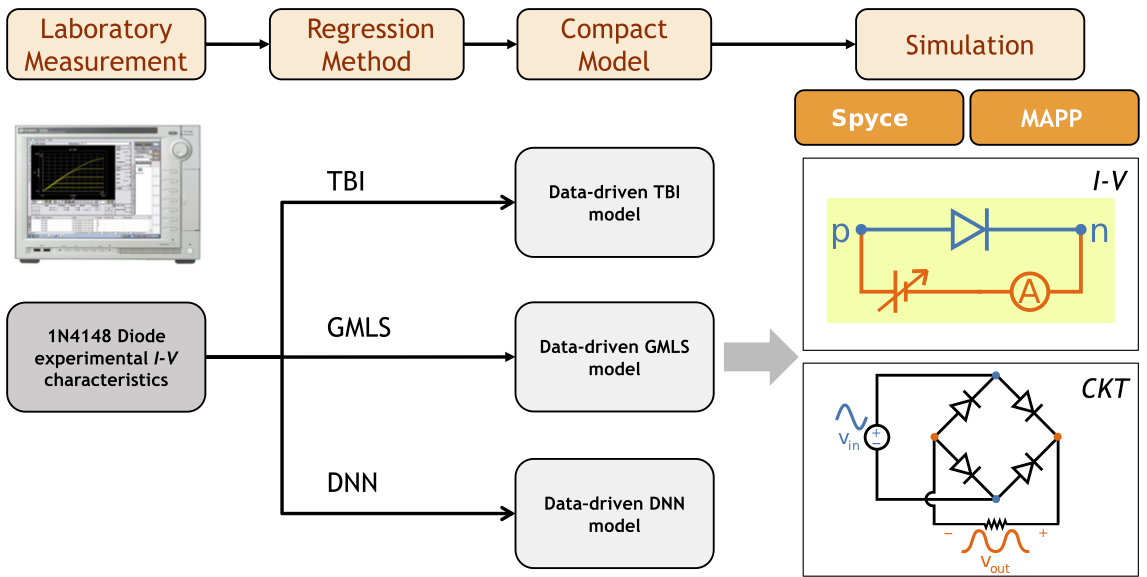
As shown in the figure, we first obtain electrical measurements in the lab. Then, we apply our three different regression methods to this data, thereby generating three different sets of data-driven compact models for the device. We then simulate these data-driven compact models to obtain their characteristics, and we also simulate circuits where such models are deployed. Circuit simulations are then compared against laboratory measurements.
Software: We have implemented the entire workflow of Figure 1 both in MATLAB and in Python. For TBI, we use two tools (1) STEAM [11, 12], an open-source MATLAB tool developed at UC Berkeley, and (2) a Python implementation of cubic splines developed for this work. For GMLS, we use the open-source Compadre toolkit [33], available as a Python package. For DNNs, we use TensorFlow [34], an open-source tool available as a Python library. And for compact model and circuit simulations, we use: (1) the Berkeley Model and Algorithm Prototyping Platform (MAPP) [35], an open-source circuit simulator written in MATLAB, and (2) Spyce, a Python-based research circuit simulator developed at Sandia National Laboratories.
2.2 A compact p-n junction diode model
A p-n junction diode has two terminals labeled and , with serving as the “reference” terminal. The voltage difference between and is denoted , and the current flowing into the diode at the non-reference terminal is denoted . The current flowing into the reference terminal is . A compact diode model is a mapping that gives the diode current as a function of the applied voltage, i.e., . Constructing a compact diode model thus boils down to specifying the function . In addition, the derivative of this function with respect to is required by the non-linear solver in the circuit simulator.
Remark 2.1.
In traditional compact models, is usually given by an analytic expression and a set of parameters that represent physical constants and/or variables that can be used to calibrate to data. As a result, the derivative of can be obtained by automatic differentiation (AD), and does not have to be provided as part of the model [36]. A typical example is the Shockley diode equation [37],
| (1) |
Here, is the reverse bias saturation current, is the thermal voltage, and is the “quality factor”, a non-physical parameter used to account for imperfect p-n junctions in real diodes. AD may also be applied to some parametric regression models for , such as TBI. However, AD is not applicable to non-parametric regression such as GMLS, in which case the compact model must also provide its derivative. As a result, the accuracy of the regression fit for alone is not enough to ensure the quality of such models; testing them in actual circuits should be an integral part of the development and validation process.
In contrast to a traditional compact model such as (1), data-driven models estimate and its derivative by applying a regression technique to a dataset . The dataset contains measurements of the device’s characteristic curve and corresponds to an matrix of real numbers.
2.3 measurements of a 1N4148 diode

The characteristic of a device is a basic set of electrical measurements and a fundamental way to understand the performance of various materials and devices under test (DUT). measurements obtain the current vs. voltage characteristic (denoted above) of a device by applying a series of voltage stimuli to the device and measuring the resulting current responses. For this work, we used a Keysight B1505A Parametric Analyzer on a 1N4148 diode specimen to obtain . This parametric analyzer uses Source Measurement Units (SMUs) that combine a current source, a voltage source, an ammeter, and a voltmeter into a single unit; see Figure 2 for a schematic. We chose the B1505A’s HPSMU (High Power Source Measurement Unit) for its ability to supply ample current over an extended voltage range while maintaining adequate measurement resolution.
For this work we sampled the curve at points, resulting in a dataset given by a matrix of real numbers. The voltage stimuli ranged from to , in increments ranging between and . The non-uniformity of the voltage increments is due to rounding errors and the fact that the measurements have inherent noise and stability issues, and are at the limit of forced voltage step resolution.
3 Core techniques for developing data-driven compact models
In this section, we apply three different regression techniques to the dataset above, to develop three different sets of data-driven compact device models for the 1N4148 diode.
3.1 Table-Based Interpolation (TBI) devices
A TBI diode compact model is a function that smoothly interpolates the data points defined by the rows of . There are many ways to construct such a function – including cubic splines, Chebyshev polynomials, and Barycentric Lagrange interpolation [10, 38]. In this paper, we use cubic splines; they are simple to describe and construct, they produce robust, -regular compact models that converge well in circuit simulations, and they offer inexpensive compact model evaluation as well as derivative computation as they only require cheap univariate cubic polynomial evaluation (with pre-computed coefficients that can be stored and looked up very efficiently). Examples of such cubic spline driven TBI compact models can be found in [11] and [12].
Remark 3.1.
A table-based model for devices with more than two terminals involves multivariate cubic spline interpolation. The main drawback of such models is that they require electrical data sampled over a rectangular grid of voltages and cannot be easily extended to scattered electrical data. This is not an issue for the univariate splines considered in this work.
Below, we briefly review the construction of the univariate cubic splines used in this work. To improve convergence of the resulting compact models in circuit simulations, our development differs in important ways from standard splines found in the literature such as natural splines.
To declutter notation, just for this subsection we switch to labeling the data points in as , . Thus, we have that , , and for . Likewise, . Without loss of generality, we assume that .
The voltage measurements induce a partition of the -axis into intervals , , , , , . We refer to the first and last interval as “boundary” intervals and the rest as “interior” intervals. A cubic spline defined with respect to this partition is a piecewise cubic polynomial which interpolates the data , , and has continuous first and second derivatives, i.e., it is of class . We denote the restriction of to the interval above as , for . Succinctly,
To determine the polynomial coefficients defining the cubic spline segment on each interval, we enforce the following constraints:
-
•
and ; : interpolation ( constraints).
-
•
; : continuity of first derivatives ( constraints).
-
•
; : continuity of second derivatives ( constraints).
-
•
and : linearity at boundary intervals ( constraints).
These conditions are sufficient to determine a unique, globally piecewise cubic interpolant of the data in . In practice, given the electrical measurements , the constraints above are used to pre-compute and store the coefficient set in memory.
To evaluate the compact model, i.e., to compute and at a query point , one first locates the interval containing and retrieves the four coefficients corresponding to the restriction of to that interval. Then the corresponding cubic polynomial and its derivative are calculated and returned.
3.2 GMLS devices
GMLS is a non-parametric regression approach for approximating linear functionals from scattered data [13]. Here, we use GMLS to estimate and from the data . Below, we describe the basics necessary for this task and refer to [13] for further details.
Consider a function with domain , a point cloud of size , with a fill distance , and a collection of point samples on the cloud. Let denote the set of all real polynomials of degree less than or equal to with dimension and basis . Finally, will denote a radially symmetric kernel function that is at least and whose support is contained in for some real .
Given a point , GMLS computes approximations and that are exact for all (polynomial reproduction) in two steps. To describe these steps, let be a diagonal matrix with element . Let , the matrix with element ; ; . And let be the Euclidean norm on weighted by . The two GMLS steps are:
Step 1. Computing the GMLS coefficient vector. Solve the weighted least-squares problem
| (2) |
Step 2. Computing the GMLS approximants. Set222The GMLS derivative approximation in (3) appears to violate the product rule and for this reason it was often referred to as the “diffuse derivative approximation” in the literature; see [39]. This confusion stems from misconstruing how the GMLS approximation works and assuming (erroneously) that is defined by differentiating . In fact, the GMLS derivative approximation is derived independently of the GMLS field approximation and does not involve differentiation of the latter; see [13].
| (3) |
To evaluate the GMLS compact diode model at a given query point , we proceed as follows. If , we associate the first and the second columns of with a point cloud and a sample set , respectively, solve (2) and define and according to (3). If , we evaluate and as follows. Let be the point from that is closest to . Note that is either or . We then set
respectively, where and are the GMLS estimates at .
In this work, we use the Compadre toolkit [33] for performant implementation of GMLS, with polynomial orders , and kernel , with and . Compadre uses an adaptive procedure to adjust until is guaranteed to contain enough points to ensure the desired degree of polynomial reproduction. For real polynomials and quasi-uniform point clouds, the number of points selected by this procedure does not exceed .
Compadre solves the weighted least-squares problem (2) using QR factorization, which formally requires flops [40, p.240]. However, the actual number of non-zero rows in equals the number of points selected by Compadre’s adaptive procedure and is bounded by , , i.e., it is orders of magnitude less than the size of the dataset . As a result, the actual cost per model evaluation is rather than . In practice, we did not observe noticeable differences in the performance of GMLS compact models as we increased the polynomial degree from 1 to 3.
3.3 DNN devices
In this work, we use a simplified DNN definition from [41]. Let and be two natural numbers defining the input dimension and the depth of the network, respectively. Consider a set of natural numbers such that , and a set of matrix-vector tuples , such that and . The elements of and are usually called the weights and the biases of the DNN respectively. Finally, let be a non-linear “activation” function. The action of the resulting DNN on an input vector is defined as
| (4) |
where is applied component-wise. We denote the transformation of the input vector by the DNN as , that is, . The mapping defines a global non-linear function parameterized by the unknown weights and biases . To determine these parameters one “trains” the network by solving a constrained optimization problem,
| (5) |
where is a “loss” function measuring the mismatch between the network’s output and the training output, is a non-linear constraint operator, is a set of training inputs, and are the corresponding outputs. We refer to the pair as the training set and denote it by . In this work, we train the neural network model using Adam, a variant of stochastic gradient descent, with a maximum of epochs.
For classification tasks, the non-linearity of is used to transform input datasets representing different classes into linearly separable sets. In contrast, here we shall use (4) as a regression tool to build a compact diode model from measurements. To that end, we set the input dimension , the output dimension and define as the mean square (MSE) error, a common choice for regression tasks. Furthermore, since circuit simulations require differentiable compact models, we only consider smooth activation functions and forego the widely used piecewise linear ReLU activation. As a constraint operator , we use non-negativity of the weights to ensure monotonicity of the function , as required by the physics of p-n junction diodes.
We train the network using three different options for the training set . The first one is , i.e., the original set of measurements with bounding box . The second option is the transformed dataset , where
| (6) |
| (7) |
with , , , and . The last option is the partially transformed set , i.e., only is transformed, not . For the numerical examples, we set , , , and . Given a training set the training process yields an instance of (4) which we label as . The data-driven compact device model is then defined as
Training DNNs on appropriately transformed electrical measurement data is one of the key ideas in this paper. Our results in Section 4 show that this strategy consistently produces DNN compact models that provide accurate data fit and perform well in circuit simulations.
The heuristics supporting the application of transformations is motivated by the physics of p-n junction diodes: when , is a very small, negative current (in our dataset, this current ranged from about nano-Amperes to micro-Amperes). To mitigate the inability of the MSE loss function to differentiate between such small values, we transform the current in the reverse bias regime roughly as . In so doing, a negative nano-Ampere current transforms into and a negative micro-Ampere becomes a . To preserve the negativity of the transformed currents, we shift them by a constant negative value; for example, if the shift is , a negative nano-Ampere and a negative micro-Ampere transform into and respectively. Such large values are easily resolvable by the MSE loss function, and hence the resulting DNNs tend to match the training data more accurately.
Conversely, when , is usually a positive current than takes on a much wider range of values (in our dataset, this current ranged from pico-Amperes to milli-Amperes). To resolve these values with the MSE loss function, we again apply a log transformation, followed by a shift so that the positivity of is preserved. For instance, with a shift of , a pico-Ampere becomes a 2 and a milli-Ampere transforms into an 11.
However, since we have used different transformations for and , we will have a discontinuity at , which can cause convergence problems in circuit simulations. To get around this, we choose a small interval around , apply the respective transformations only outside this interval, and apply a continuity-preserving linear transformation within this interval. This approach ensures that an MSE loss function in conjunction with the transformed set resolves both positive and negative p-n junction currents very well, leading to a much better fit.
Configuring and training a DNN involves choosing several parameters, such as the number of hidden layers , the number of neurons per hidden layer, the activation function, whether or not to use a kernel constraint, whether or not to transform , and whether or not to transform . In this work, we experimented with DNNs containing and hidden layers, with , , , , or neurons per hidden layer, and different activation functions (eLU, sigmoid, and tanh). Taken together with the binary choices of whether to have a kernel constraint, transform , and/or transform , this corresponds to a parameter space of size . We systematically explored this space, generating all DNN compact models. Then we simulated them all using Spyce, to determine their characteristics as well as their performance in a bridge rectifier circuit. We do not need to discuss all the DNNs here; a carefully chosen representative sample of “interesting” DNNs (summarized in Table 1) suffice to highlight the key points we wish to make.
| Model | |||||
|---|---|---|---|---|---|
| M1-50-E | eLU | 1 | 50 | Non-neg | |
| M2-50-E | eLU | 2 | 50 | Non-neg | |
| M1-50-S | sigmoid | 1 | 50 | Non-neg | |
| M2-50-S | sigmoid | 2 | 50 | Non-neg | |
| M1-50-T | tanh | 1 | 50 | Non-neg | |
| M1-50-S-neg | sigmoid | 1 | 50 | None | |
| M2-50-S-neg | sigmoid | 2 | 50 | None | |
| M1-10-E-VI | eLU | 1 | 10 | Non-neg | |
| M2-10-E-VI | eLU | 2 | 10 | Non-neg | |
| M1-10-E-VI-neg | eLU | 1 | 10 | None | |
| M2-10-E-VI-neg | eLU | 2 | 10 | None | |
| M1-10-T-VI | tanh | 1 | 10 | Non-neg | |
| M2-10-T-VI | tanh | 2 | 10 | Non-neg | |
| M2-25-T-VI | tanh | 2 | 25 | Non-neg | |
| M2-50-T-VI | tanh | 2 | 50 | Non-neg | |
| M2-100-T-VI | tanh | 2 | 100 | Non-neg |
4 Results
In this section, we carry out two types of simulations for each data-driven diode compact model: we (1) produce its characteristics, and (2) simulate a bridge rectifier circuit (schematic shown at the bottom right of Figure 1) that uses instances of the model. The input signal to the rectifier is a sine wave with frequency Hz and phase shift approximately . This simulation provides device model validation at a circuit level. We compare the results of both simulations against laboratory data.
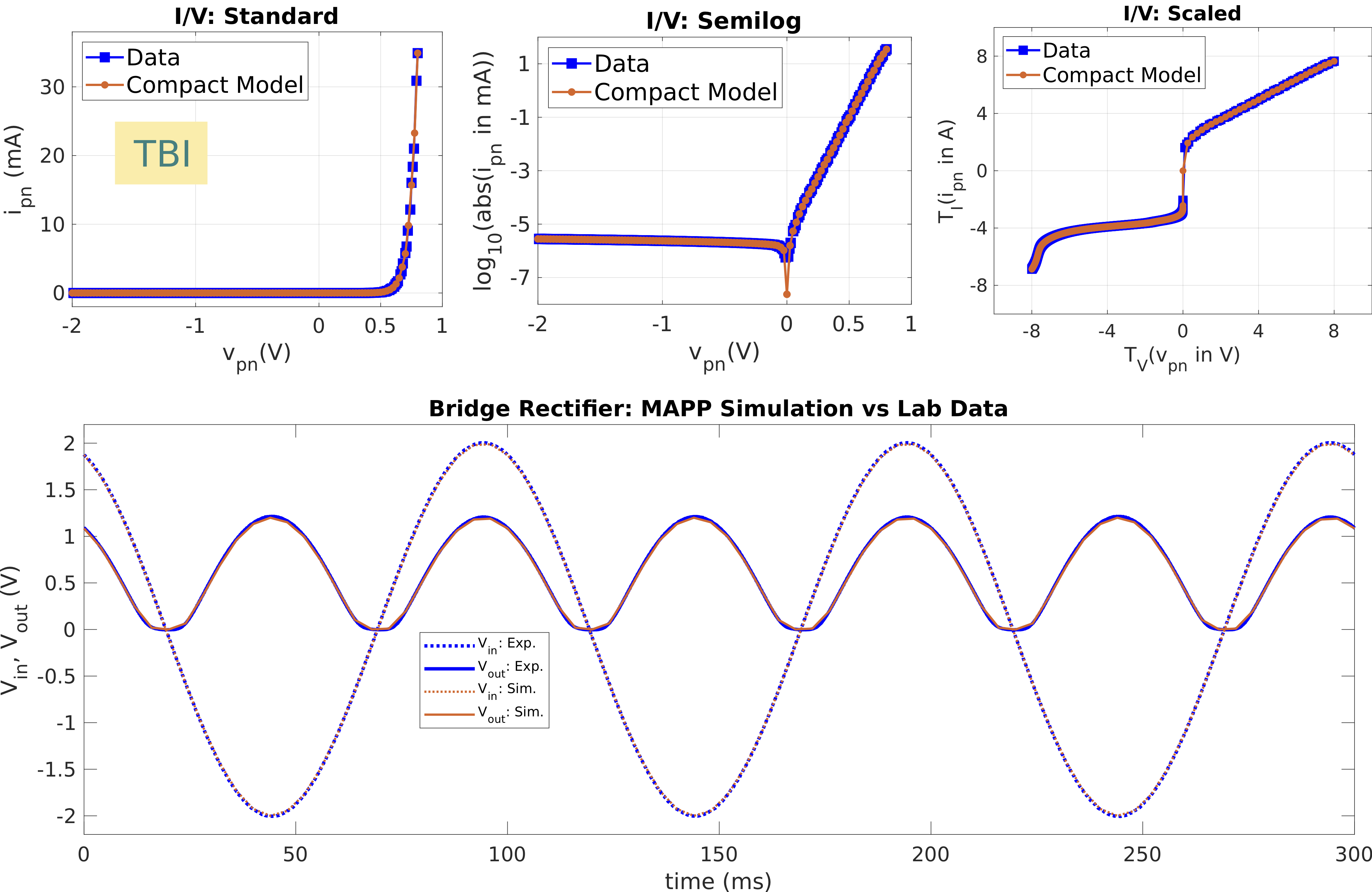
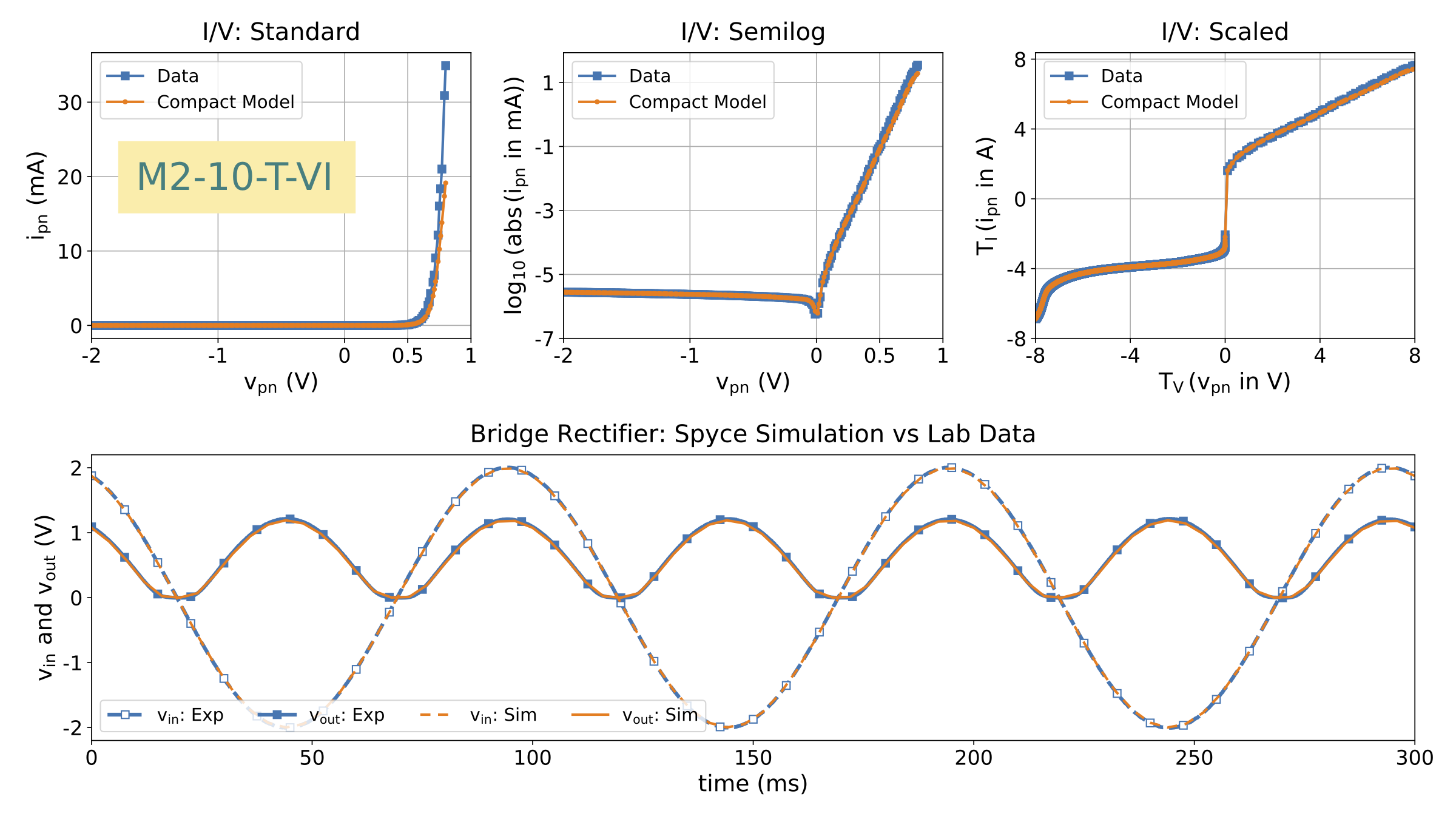
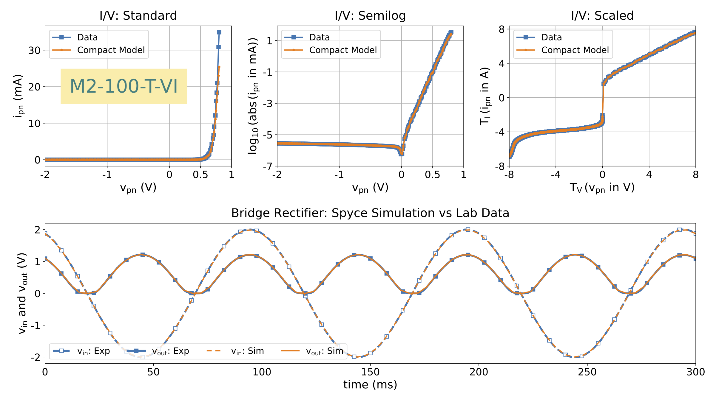
To visualize how well a data-driven diode compact model matches measured data, we arrange results in plots containing top sub-plots and bottom sub-plot (see, for example, Figure 3). The top sub-plots show the characteristics of the compact model, overlaid on top of laboratory data, using three different “data views” defined as follows:
-
•
Standard (top-left sub-plot): is plotted as a function of for .
-
•
Semilog (top-middle sub-plot): is plotted as a function of for .
- •
Together, the three data views provide a comprehensive picture of the model: the standard view highlights the forward bias regime where the diode conducts positive, exponentially-growing current for positive . The semilog view highlights the “zero crossing point”, where the diode transitions from reverse bias (where it conducts very little current) to forward bias. The scaled view exposes the entire region of operation of the diode, from avalanche breakdown (where starts to become more and more negative at very low , risking irreversible damage to the device) all the way to forward bias.
The bottom sub-plot in each figure shows a bridge rectifier circuit simulation using instances of the data-driven diode compact model (see schematic at the bottom right of Figure 1), overlaid on top of laboratory data.
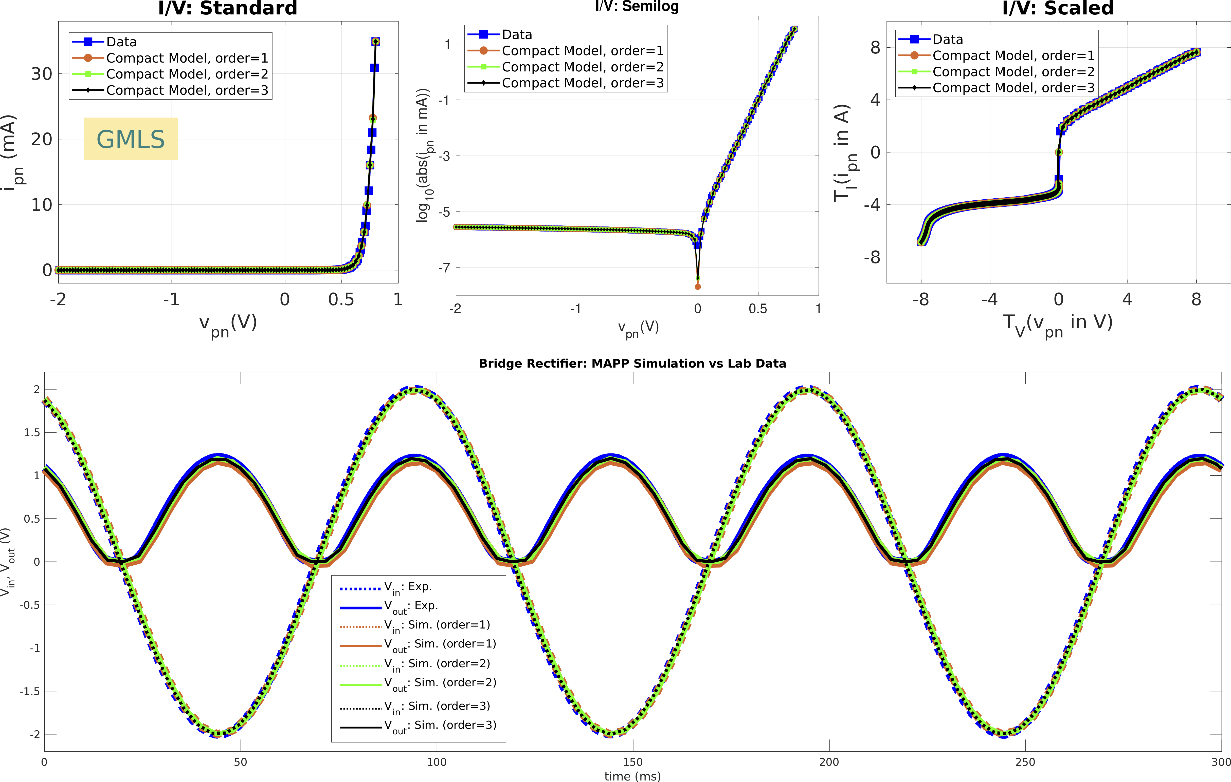
Figure 3 shows simulation results for a cubic spline TBI diode compact model, generated via STEAM and MAPP. Figure 4 shows the same for GMLS compact models (with polynomial orders 1, 2, and 3). In both cases, we see that the data-driven models are in excellent agreement with laboratory data. We do not show results for TBI and GMLS models generated via Spyce, because they are virtually identical to the MAPP/STEAM results shown here.
We now turn to compact DNN models. Using the original dataset as the training set failed to produce even a single accurate DNN compact model. For all parameter choices described in Section 3.3, the learned DNN models were both inaccurate and unphysical.


Figures 5–8 illustrate these failures using representative examples drawn from the 240 combinations examined in this work. Figure 5 shows typical results obtained with eLU, sigmoid and tanh activation functions for networks having one hidden layer and enforcing non-negative kernel constraints. Figures 6 and 7 compare the first two examples from Figure 5 with networks having one additional hidden layer. While the standard data views on these plots suggest regression fit improvements as a result of introducing an extra hidden layer, the semilog and scaled data views reveal that this is not necessarily the case. In particular, we observe significant qualitative changes in the behavior of the compact DNN models that are counterintuitive.


For example, the semilog view shows that M1-50-E does not have a zero switching point whereas M1-50-S does. Interestingly, with two hidden layers, the roles reverse and now M2-50-E exhibits a zero switching point, whereas M2-50-S does not. Note, however, that the zero switching for M2-50-E occurs at a highly non-physical value of almost .


Figure 8 shows results with two DNN compact models that do not enforce the non-negative kernel constraint. In the case of M1-50-S-neg, which has a single hidden layer, the unphysical nature of the model can already be seen in the standard data view plot. The same view suggests that increasing the number of hidden layers to two seems to dramatically improve the model. However, the semilog and scaled data views again confirm that the resulting model M2-50-S-neg is unphysical. In particular, we see that similar to M1-50-S-neg, the model has multiple zero switching points, unlike the real diode which has only one.
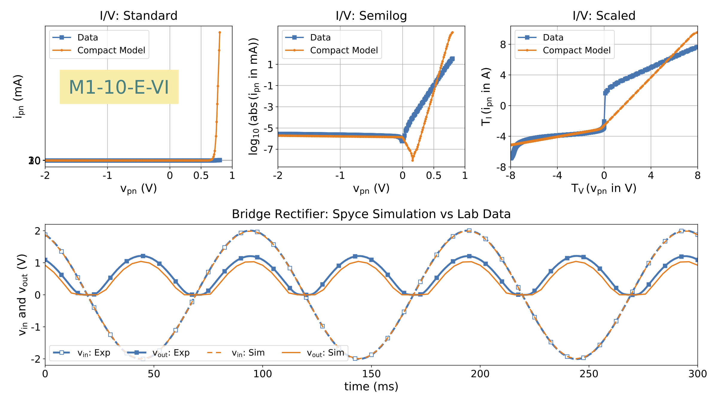
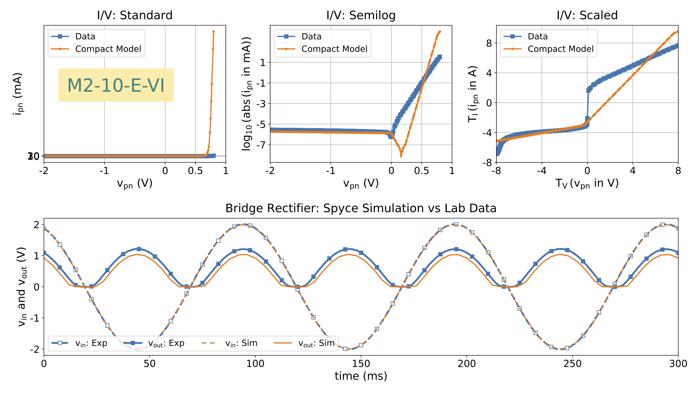
Our results indicate that DNN performance markedly improves by switching the training set to the transformed dataset . However, an important takeaway is that not all activation functions lead to satisfactory compact models. In particular, we found that eLU activation performed much worse than sigmoid or tanh. For example, the top plot in Figure 9 shows simulations of the M1-10-E-VI compact model; from the standard characteristic plot, it is apparent that the model greatly overestimates the current in the forward bias region. Indeed, at , the current predicted by the model is so high that the Y-axis tick labels on the standard view have all been compressed to the point that they overlap one another. Still, the transformations of the training set ensure that the model behaves well and has good convergence properties during circuit simulation; the circuit simulation plot shows that the model even gets reasonably close to matching laboratory data when it comes to circuit behaviour. As in other cases, we did not observe a significant improvement in the model when the number of layers was increased to two; see the results in the bottom part of Figure 9.
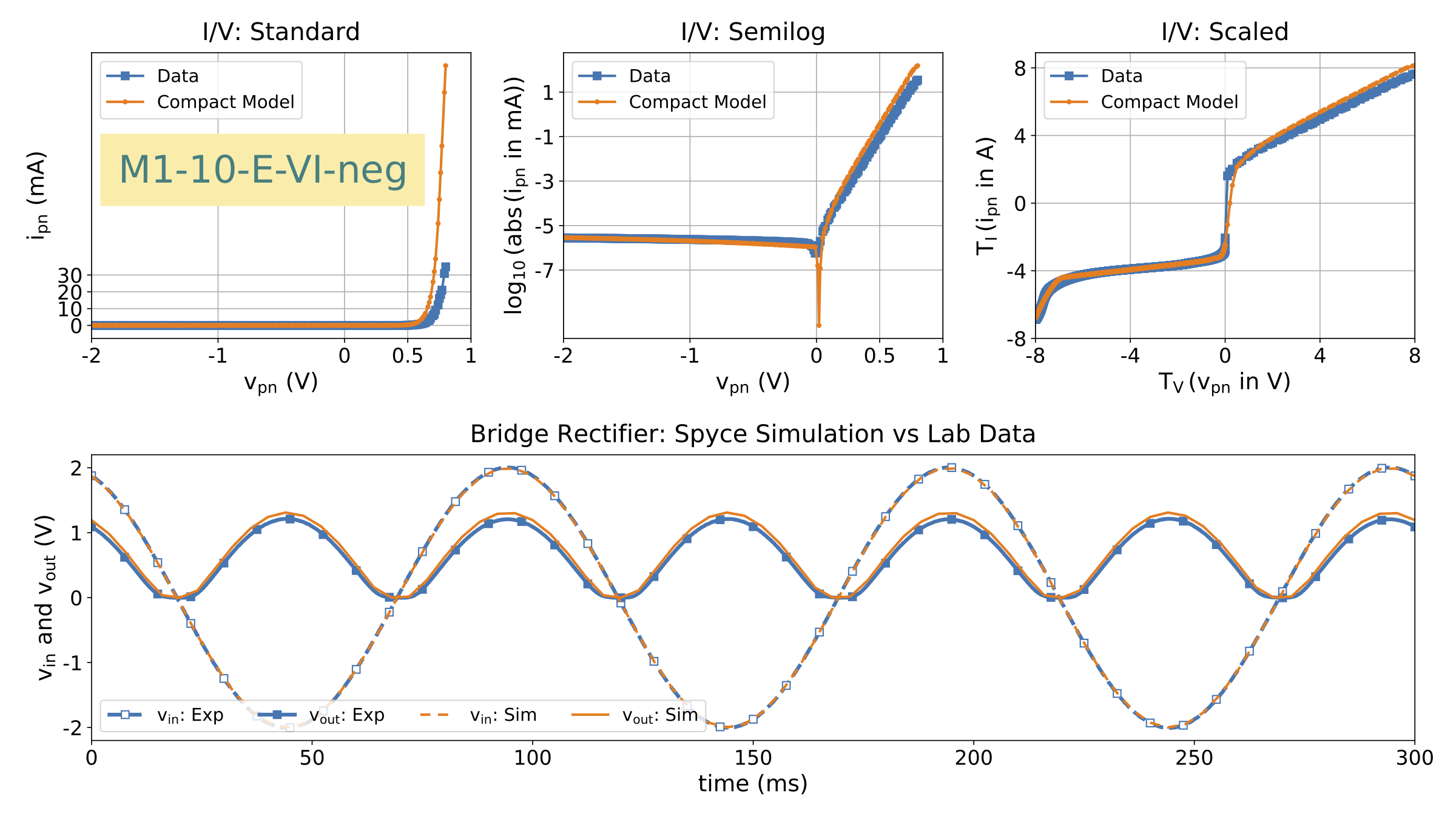
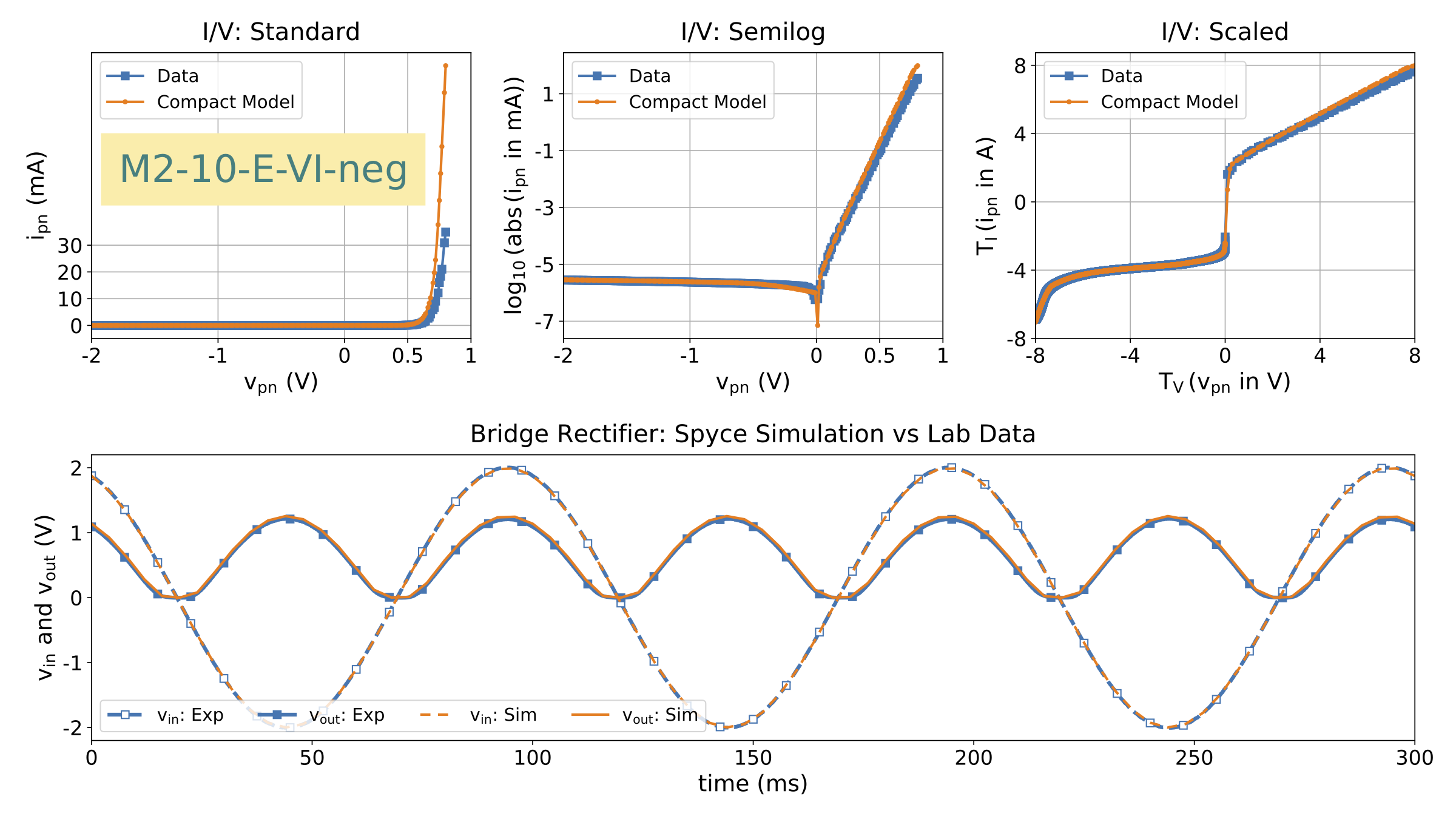
Figure 10 shows an interesting corner case: with eLU activation and data transformations, it looks like removing the non-negative weight constraint actually helps the model become more accurate, both in its characteristic and in circuit simulations.
We hypothesize that this behavior is caused by eLU. Recall that eLU is the identity function for positive inputs and an exponential converging to a negative value for negative inputs. Thus, if the weights in the DNN are constrained to be positive, the DNN’s behavior is constrained to be close to linear, which is a bad fit for a diode. Thus, in this special case, allowing negative weights actually helps the DNN become more non-linear, and hence mimic the data more closely.
With regard to eLU, it is worth pointing out that besides getting better models without the non-negative kernel constraint, this was one of the few cases where increasing the number of layers actually improved the model fit. As Figure 10 shows, the M2-10-E-VI-neg model still overestimates the current in the forward bias region, but to an extent noticeably smaller than M1-10-E-VI-neg. This improvement in the characteristic of M2-10-E-VI-neg translates into more accurate circuit simulations as well; in fact, the difference in the circuit simulations between M2-10-E-VI-neg and M1-10-E-VI-neg is visible to the naked eye, as seen from the two circuit simulations shown in Figure 10.
By far, our most positive DNN finding is that combining sigmoid or tanh activation with data transformations can produce extremely accurate, physically consistent, and efficient DNN models. The top plot in Figure 11 shows this for the M1-10-T-VI case; with just a single hidden layer and 10 neurons, this tanh activated DNN is able to model all aspects of the diode’s characteristic very well, and perform very accurately in circuit simulations as well. In fact, as evidenced by the results in the bottom part of Figure 11 and the plots in Figure 12, increasing the number of layers and/or neurons does not significantly increase model accuracy; the base model with just neurons and a single hidden layer is already so good that it is difficult to improve upon it. We found that similar results held true with sigmoid activation. Also, combining tanh/sigmoid with data transformations proved very resilient to other training parameters; no matter what we chose for the other parameters, the resulting DNN models were always accurate and converged robustly (producing plots almost indistinguishable from those in Figures 11 and 12).
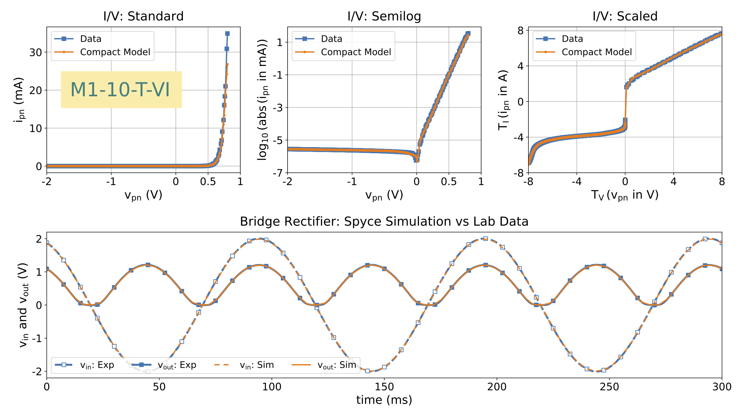

Finally, we found that applying the data transformation to was far more critical than applying it to . In fact, the performance of the DNN compact model showed only minor degradation (often invisible in plots) when we applied but omitted applying to the training dataset.
-
•
Data transformations are critical to obtaining accurate and physically consistent DNN compact models;
- •
-
•
Generally, increasing the number of layers and/or neurons is not guaranteed to improve the model and can prompt significant qualitative changes in its behavior.
Also, we note that even if the standard characteristic of a data-driven compact model appears to match laboratory data satisfactorily, the characteristic needs to be viewed on a semilog plot, as well as on a scaled plot, to assess how well the model represents the physics of the device. For example, although all models in Figure 5 look reasonable on the standard plot, the semilog and scaled plots reveal unphysical behaviours such as current overestimation in both forward and reverse bias, as well as the absence of or shifts in the zero crossing point.
5 Conclusions
In this paper, we investigated three different regression approaches to develop data-driven compact models for a 1N4148 diode from laboratory measurements. The first two (TBI via cubic splines and GMLS) are examples of local parametric and non-parametric regression models. Simulation results demonstrate that both of these approaches deliver accurate and physically consistent compact device models that show excellent agreement with laboratory measurements in all device operational regimes. Furthermore, both compact models performed robustly in circuit simulations; the simulated output of a bridge rectifier circuit was in excellent agreement with laboratory measurements. The TBI model has higher memory requirements than GMLS but faster model evaluation. The use of the performant Compadre toolkit however enables highly efficient GMLS computation. As a result, both models can be deemed appropriate for the one-junction device considered in this work.
For two-junction devices that will be the subject of a forthcoming paper, TBI via multivariate splines will require data on a rectangular grid, whereas GMLS will not have such a restriction. For such devices, GMLS may be more appropriate for scattered electrical measurements.
Our experiences with DNNs highlight the potential of this regression technique for compact model development. In particular, using data transformations and sigmoid/tanh activation, we were able to accurately regress a complex dataset spanning multiple scales and comprising more than 9000 data points by a shallow network with just 10 neurons. This makes our DNN compact model by far the most memory efficient of all three kinds of data-driven models considered here; unlike DNNs, TBI and GMLS models both require memory of the order of the size of the entire dataset. This could be a significant advantage for DNNs when modeling devices with more than one p-n junction. DNN models are also computationally efficient: being a global regression, DNNs do not require dataset searches as TBI and GMLS models do; their main cost is a few evaluations of their non-linear activation functions.
At the same time, applying DNNs to approximate physics-based models requires deeper understanding of their properties as regression tools. Although DNNs potentially have the best generalizability of all the models considered in this work, their regression accuracy depends on a complex interplay between depth, width, activation functions, loss functions, constraint operators, etc. Although we have gained some insights on training DNNs for compact model development (as described in Section 4), we believe that our understanding is far from complete, and that devices with more than two terminals will pose significant additional challenges in identifying the best combinations of data transformations, architectures, constraint operators, etc.
Furthermore, circuit simulations underscore the importance of ensuring correct physical behavior from data-driven compact models. For example, a good fit in the forward bias region is not enough to ensure robust and physically correct circuit simulations; this requires accurate representation of the zero crossing and the leakage current in the reverse bias regime as well. Without these features, circuit simulations are likely to be unphysical at best, and completely meaningless at worst.
The results in this paper suggest that data transformations are currently the most effective heuristics for achieving acceptable accuracy in data-driven DNN compact diode models. The transformations developed in this work aim to reduce the vast difference in scales present in the diode characteristic curve, which enables good data fits using a standard MSE loss function. A custom loss function that adapts to multiscale data is another potential option to improve DNN fit. We plan to pursue this work in the future.
Acknowledgments
Supported by the Laboratory Directed Research and Development program at Sandia National Laboratories, a multimission laboratory managed and operated by National Technology and Engineering Solutions of Sandia, LLC., a wholly owned subsidiary of Honeywell International, Inc., for the U.S. Department of Energy’s National Nuclear Security Administration under contract DE-NA-0003525. This paper describes objective technical results and analysis. Any subjective views or opinions that might be expressed in the paper do not necessarily represent the views of the U.S. Department of Energy or the United States Government.
The work of P. Bochev has also been supported by the U.S. Department of Energy, the Office of Science, and the Office of Advanced Scientific Computing Research under Award Number DE-SC-0000230927, as well as the Collaboratory on Mathematics and Physics-Informed Learning Machines for Multiscale and Multiphysics Problems (PhILMs) project.
References
- [1] L. W. Nagel. SPICE2: A computer program to simulate semiconductor circuits. PhD thesis, EECS Department, University of California, Berkeley, 1975.
- [2] E. R. Keiter, K. V. Aadithya, T. Mei, T. V. Russo, R. L. Schiek, P. E. Sholander, H. K. Thornquist, and J. C. Verley. Xyce parallel electronic simulator: Users’ guide, version 6.11. Technical Report SAND2019-5949, Sandia National Laboratories, Albuquerque, NM, 2019.
- [3] E. R. Keiter, K. V. Aadithya, T. Mei, T. V. Russo, R. L. Schiek, P. E. Sholander, H. K. Thornquist, and J. C. Verley. Xyce parallel electronic simulator: Reference guide, version 6.11. Technical Report SAND2019-5950, Sandia National Laboratories, Albuquerque, NM, 2019.
- [4] https://charon.sandia.gov/index.html.
- [5] Y. S. Chauhan, D. D. Lu, S. Venugopalan, S. Khandelwal, J. P. Duarte, N. Payvadosi, A. Niknejad, and C. Hu. FinFET modeling for IC simulation and design: Using the BSIM-CMG standard. Academic Press, 2015.
- [6] W. Liu and C. Hu. BSIM4 and MOSFET modeling for IC simulation. World Scientific, 2011.
- [7] W. Liu and C. Hu. BSIM3v3 MOSFET model. 9(03):671–701, 1998.
- [8] https://en.wikipedia.org/wiki/1N4148_signal_diode.
- [9] https://www.diodes.com/assets/Datasheets/ds12019.pdf.
- [10] C. de Boor. A Practical Guide to Splines. Springer-Verlag New York, 1978.
- [11] A. Gupta, T. Wang, A. G. Mahmutoglu, and J. Roychowdhury. STEAM: Spline-based tables for efficient and accurate device modelling. In ASPDAC ’17: The Asia and South Pacific Design Automation Conference, pages 463–468, 2017.
- [12] A. Gupta. Table-based device modeling: Methods and applications. Master’s thesis, EECS Department, University of California, Berkeley, 2018.
- [13] H. Wendland. Scattered data approximation. Cambridge University Press, 2004.
- [14] C. Jiun-Shyan, H. Michael, and C. Sheng-Wei. Meshfree methods: Progress made after 20 years. 143(4):04017001, 2017.
- [15] S. R. Slattery. Mesh-free data transfer algorithms for partitioned multiphysics problems: Conservation, accuracy, and parallelism. Journal of Computational Physics, 307:164–188, 2016.
- [16] H.-J. Bungartz, F. Lindner, B. Gatzhammer, M. Mehl, K. Scheufele, A. Shukaev, and B. Uekermann. PRECICE: A fully parallel library for multi-physics surface coupling. Computers & Fluids, 141:250–258, 2016. Advances in Fluid-Structure Interaction.
- [17] I. Goodfellow, J. Bengio, and A. Courville. Deep Learning. The MIT Press, 2016.
- [18] Y. LeCun, Y. Bengio, and G. Hinton. Deep learning. Nature, 521:436–444, 2015.
- [19] Y. Bar-Sinai, S. Hoyer, J. Hickey, and M. P. Brenner. Learning data-driven discretizations for partial differential equations. Proceedings of the National Academy of Sciences, 116(31):15344–15349, 2019.
- [20] M. Raissi, P. Perdikaris, and G. E. Karniadakis. Physics informed deep learning (part 1): Data-driven solutions of non-linear partial differential equations. arXiv preprint arXiv:1711.10561, 2017.
- [21] A. H. Zaabab, Q.-J. Zhang, and M. S. Nakhla. Analysis and optimization of microwave circuits and devices using neural network models. In IEEE MTT-S International Microwave Symposium Digest, volume 1, pages 393–396, May 1994.
- [22] A. H. Zaabab, Q.-J. Zhang, and M. S. Nakhla. A neural network modeling approach to circuit optimization and statistical design. IEEE Transactions on Microwave Theory and Techniques, 43(6):1349–1358, June 1995.
- [23] P. B. L. Meijer. Neural network applications in device and sub-circuit modelling for circuit simulation. PhD thesis, Department of Chemical Engineering and Chemistry, Technische Universiteit Eindhoven, 1996.
- [24] V. B. Litovski, Ž. Mrčarica, and T. Ilić. Simulation of non-linear magnetic circuits modelled using artificial neural network. Simulation Practice and Theory, 5(6):553–570, 1997.
- [25] M. Andrejević and V. B. Litovski. Electronic circuits modeling using artificial neural networks. Journal of Automatic Control, University of Belgrade, 13(1):31–37, 2003.
- [26] X. Chen, G. F. Wang, W. Zhou, Q. L. Zhang, and J. F. Xu. Application of neural networks for integrated circuit modeling. In Advances in Neural Networks, volume 3973, pages 1304–1312, 2006.
- [27] D. Gorissen, L. D. Tommasi, and K. Crombecq. Sequential modeling of a low noise amplifier with neural networks and active learning. Neural Computing & Applications, 18:485–494, 2009.
- [28] Z. Chen, M. Raginsky, and E. Rosenbaum. Verilog-A compatible recurrent neural network model for transient circuit simulation. In EPEPS ’17: The IEEE Conference on Electrical Performance of Electronic Packaging and Systems, pages 1–3, 2017.
- [29] A. H. Zaabab, Q.-J. Zhang, and M. S. Nakhla. Device and circuit-level modeling using neural networks with faster training based on network sparsity. IEEE Transactions on Microwave Theory and Techniques, 45(10):1696–1704, Oct 1997.
- [30] H. B. Hammouda, M. Mhiri, Z. Gafsi, and K. Besbes. Neural-based models of semiconductor devices for SPICE simulator. American Journal of Applied Sciences, pages 385–391, 2008.
- [31] Y. Lei, X. Huo, and B. Yan. Deep neural network for device modeling. In EDTM ’18: The IEEE Electron Devices Technology and Manufacturing Conference, pages 154–156, 2018.
- [32] M. Li, O. İrsoy, C. Cardie, and H. G. Xing. Physics-inspired neural networks for efficient device compact modeling. IEEE Journal on Exploratory Solid-State Computational Devices and Circuits, 2:44–49, Dec 2016.
- [33] P. Kuberry, P. Bosler, and N. Trask. Compadre toolkit, February 2019.
- [34] M. Abadi, A. Agarwal, P. Barham, E. Brevdo, Z. Chen, C. Citro, G. S. Corrado, A. Davis, J. Dean, M. Devin, S. Ghemawat, I. Goodfellow, A. Harp, G. Irving, M. Isard, Y. Jia, R. Jozefowicz, L. Kaiser, K. Kudlur, J. Levenberg, D. Mané, R. Monga, S. Moore, D. Murray, C. Olah, M. Schuster, J. Shlens, B. Steiner, I. Sutskever, K. Talwar, P. Tucker, V. Vanhoucke, V. Vasudevan, F. Viégas, O. Vinyals, W. Warden, M. Wattenberg, M. Wicke, Y. Yu, and X. Zheng. TensorFlow: Large-scale Machine Learning on heterogeneous systems, 2015. Software available from tensorflow.org.
- [35] T. Wang and J. Roychowdhury. Multiphysics modelling and simulation in Berkeley MAPP. In NEMO ’16: The IEEE MTT-S International Conference on Numerical Electromagnetic and Multiphysics Modeling and Optimization, pages 1–3, July 2016.
- [36] A. Griewank and A. Walther. Evaluating derivatives: Principles and techniques of algorithmic differentiation. SIAM, 2 edition, 2008.
- [37] W. Shockley. The theory of p-n junctions in semiconductors and p-n junction transistors. Bell System Technical Journal, 28(3):435–489, 1949.
- [38] L. N. Trefethen. Approximation theory and approximation practice, volume 128. SIAM, 2013.
- [39] D. Mirzaei, R. Schaback, and M. Dehghan. On generalized moving least squares and diffuse derivatives. IMA Journal of Numerical Analysis, 32(3):983–1000, 2012.
- [40] G. Golub and C. F. V. Loan. Matrix computations. Johns Hopkins University Press, 3 edition, 1996.
- [41] J. A. A. Opschoor, P. C. Petersen, and C. Schwab. Deep ReLU networks and high-order finite element methods. Research Report 2019-07, ETH Zurich, January 2019.