Structural, optical, and electrical properties of unintentionally doped NiO layers grown on MgO by plasma-assisted molecular beam epitaxy
)
Abstract
NiO layers were grown on MgO(100), MgO(110) and MgO(111) substrates by plasma-assisted molecular beam epitaxy under Ni-flux limited growth conditions. Single crystalline growth with a cube-on-cube epitaxial relationship was confirmed by X-ray diffraction measurements for all used growth conditions and substrates except MgO(111). A detailed growth series on MgO(100) was prepared using substrate temperatures ranging from 20 °C to 900 °C to investigate the influence on the layer characteristics. Energy-dispersive X-ray spectroscopy indicated close-to-stoichiometric layers with an oxygen content of at.% and at.% grown under low and high O-flux, respectively. All NiO layers had a root-mean-square surface roughness below 1 nm, measured by atomic force microscopy, except for rougher layers grown at 900 °C or using molecular oxygen. Growth at 900 °C led to a significant diffusion of Mg from the substrate into the film. The relative intensity of the quasi-forbidden one-phonon Raman peak is introduced as a gauge of the crystal quality, indicating the highest layer quality for growth at low oxygen fluxes and high growth temperature, likely due to the resulting high adatom diffusion length during growth. Optical and electrical properties were investigated by spectroscopic ellipsometry and resistance measurements, respectively. All NiO layers were transparent with an optical band gap around 3.6 eV and semi-insulating at room temperature. However, changes upon exposure to reducing or oxidizing gases of the resistance of a representative layer at elevated temperature was able to confirm -type conductivity, highlighting their suitability as a model system for research on oxide-based gas sensing.
I Introduction
Nickel oxide (NiO) is a transparent oxide due to the wide
band gap around 3.7 eV.Ohta et al. (2003) It crystallizes in the rock salt
crystal structure and is either unintentionally -type
conductive or insulating depending on the growth conditions.Rao and Smakula (1965)
While highly stoichiometric NiO is considered to be insulating, hole
states induced by Ni vacancies are supposed to create the unintentional
-type conductivity. The -type conductivity
can also be created intentionally by doping with Lithium.Rao and Smakula (1965); Zhang et al. (2018)
Explanations of the insulating state of NiO varied between a Mott
insulator, a charge transfer insulator, or a mixture of both.Schuler et al. (2005)
Furthermore, NiO is antiferromagnetic with a Néel temperature of about
525 KSchuler et al. (2005). Below this temperature the crystal structure
is slightly modified into a rhombohedrally distorted form bearing
angles of > 90.1° instead of 90°.Massidda et al. (1999)
However, for the present discussion which does not concentrate on
magnetic properties but on crystal growth, electrical and optical
properties we can safely neglect the small deviation from the perfect
cubic structure. The wide variety of properties made NiO thin films
an interesting material for many applications. First, NiO can be used
as an antiferromagnetic layer in giant magnetoresistive (GMR) spin
valve structuresHoshiya et al. (1994) and other magneto-electronic devices.Becker et al. (2017a)
Secondly, as a p-type transparent semiconductor it is a very
relevant material for oxide-based gas sensorsKim and Lee (2014); Miller et al. (2014)
as well as for pn-diodes and other transparent oxide
electronics.Ohta et al. (2003); Zhang et al. (2016); von Wenckstern et al. (2015) Additionally,
NiO can be used as a hole transport and electron blocking layer in
organic solar cells.Irwin et al. (2007) NiO films have already been grown
by many methods, including sputtering,Warot et al. (2001a); Becker et al. (2017b); Murphy and Hutchins (1995)
metal evaporation with oxygen or nitrogen dioxide inlet,Peacor and Hibma (1994)
pulsed laser deposition (PLD),Tachiki et al. (2000); Zhang et al. (2018) sol-gel coating,Manders et al. (2013)
or plasma-assisted molecular beam epitaxy (PA-MBE).Lind et al. (1992)
As an alloy together with MgO it is also interesting for deep-ultraviolet
photodetectors, offering a band gap tuning between 3.6 and 7.8 eV.Mares et al. (2010)
To exclude the disturbing effects of grain boundaries for
basic investigations of the material single crystalline NiO layers
are necessary. These layers can serve as model system with reduced
complexity to investigate fundamentals of NiO-based applications,
such as oxide-based gas-sensing.Rombach et al. (2016) The common rock-salt
crystal structure with similar lattice constants of MgO (0.4212 nm)
and NiO (0.4176 nm) and low lattice mismatch < 1 % makes MgO a
widely-used, suitable substrate to epitaxially grow high quality NiO
layers.Lind et al. (1992); Zhang et al. (2018) In addition, MgO was found to be a good
electron blocking layer for GaN/NiO based diodes.Wang et al. (2011)
Detailed investigations about the epitaxial growth of NiO at different
growth conditions, however, are very rare: Warot et al. studied the
growth of NiO by PLD on different orientations of MgO.Warot et al. (2001a, 2002a, b, 2002b)
Lind et al. observed single crystalline NiO films on MgO(100) by PA-MBE
only for growth temperatures up to 260°C and polycrystalline
growth for higher temperatures.Lind et al. (1992)
In this study we investigate the PA-MBE growth and properties of NiO thin films on different MgO orientations and under a wider range of growth conditions with the goal of realizing high quality single crystalline layers. Furthermore, we propose a new metrics to measure the crystalline quality of NiO using Raman spectroscopy. For all properties a reference NiO bulk sample was measured.
II Experiment
For the MBE growth, quarters of 2-inch MgO(100), MgO(110)
and MgO(111) substrates (from CrysTec GmbH) were used. For layers
grown on MgO(100) growth temperature and oxygen flux were varied with
the idea to modify the concentration of Ni vacancies. The growth temperatures
are defined by the substrate heater temperatures, measured by a thermocouple
between substrate and heating filament. A 1 µm thick layer
of sputter-deposited titanium layer on the rough backside of the substrate
improved the substrate heating by absorbing the radiation from the
heating filament. Activated oxygen was provided by flux passing a
controlled molecular oxygen through an RF plasma source directed to
the substrate. Before growth, the surface quality of all substrates
was improved by a plasma treatment in the growth chamber at various
conditions defined by temperatures ranging from 700 °C
to 900 °C, oxygen fluxes ranging from 0.3 to 3 standard
cubic centimeters per minute (sccm) at plasma powers ranging from
150 W to 300 W for 20 to 30 minutes. This treatment helps to reduce
organic contaminations at the surface and increase the surface crystalline
order. For the growth, an oxygen plasma and a nickel effusion cell
were used. As a protection of the nickel effusion cell, the temperature
was kept well below the melting point of nickel (1455 °C),
at 1380 °C. The beam equivalent pressure (BEP), which
is proportional to the particle flux, was measured by a nude filament
ion gauge positioned at the substrate location and removed before
growth. The resulting nickel BEP was between mbar
and mbar, which led to growth rates between 0.05 Å/s
and 0.09 Å/s. The growth temperature for layers grown on MgO(100)
was varied between 20 °C and 900 °C. Furthermore,
different activated oxygen fluxes were used: series one (S1) was grown
with a high oxygen flux of 1 sccm at a plasma power of 300 W with
resulting oxygen BEP of mbar. Series two
(S2) was grown with a strongly reduced active oxygen flux of 0.3 sccm
at 150 W with resulting oxygen BEP of mbar.
Higher oxygen fluxes, which should be beneficial for the formation
of Ni vacancies, led to the problem of NiO formation at the orifice
of the nickel cell, which continuously reduces the Ni flux and can
eventually lead to the complete closure of the Ni cell. In the following
the samples will be named by their series and growth temperature,
for example the sample from series 1 grown at 700 °C is
called S1-700. The layers on MgO(110) and MgO(111) were grown at 700 °C
with an oxygen flux of 1 sccm and a power of 300 W. Besides the
plasma assisted growth, one layer was grown at 700 °C
on MgO(100) with molecular oxygen and a flux of 0.3 sccm.
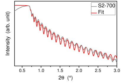
After the growth, all layers were investigated by different ex-situ methods. First, the layer thickness was determined by fitting measured X-ray reflectometry (XRR) curves assuming only the NiO layer on top of the MgO substrate. A representative XRR curve and its corresponding fit curve are shown in Fig. 1 for S2-700. The extracted thicknesses of this layer and all other layers grown with an oxygen plasma on MgO(100) are shown in Tab. 1. The extracted layer thickness of the sample grown with molecular oxygen is 39 nm. The extracted layer thickness on MgO(110) and MgO(111) are 30 nm and 35 nm, respectively. Secondly, different X-ray diffraction (XRD) scans were used to determine the epitaxial relationship between substrate and layer.
| S1 | [°C] | 250 | 450 | 700 | |
|---|---|---|---|---|---|
| [nm] | 50 | 24 | 51 | ||
| S2 | [°C] | 20 | 200 | 400 | 700 |
| [nm] | 62 | 60 | 53 | 65 |
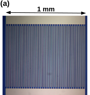
Further layer properties were investigated for the growth series on MgO(100). The effect of different growth parameters on the surface morphology was analyzed by atomic force microscopy (AFM) in the peak force tapping mode using a Bruker “Dimension edge” with the “ScanAsyst” technology. Scanning electron microscope-based energy dispersive X-ray spectroscopy (EDX) with a Zeiss ULTRA 55 was used to determine the proportion of nickel and oxygen for selected samples, using an electron energy of 3 keV and a beam current of about 1 nA. The X-ray radiation is measured and analyzed by an EDAX system with a SDD Apollo XV detector. Raman spectroscopy was utilized to assess the NiO crystal quality. The spectra were recorded at room temperature in backscattering geometry using the 325-nm line of a Cd-He ion laser and a 405-nm diode laser for optical excitation. In addition, optical characteristics were determined by spectroscopic ellipsometry measurements in the range of 1.2 to 6.5 eV for three angles of incidence (50°, 60°, 70°) to improve the reliability of the obtained dielectric functions (DFs). The DFs were obtained by multilayer modeling of the ellipsometric dataGoldhahn (2003), where the surface roughness was modeled using the Bruggeman effective medium approximation.Bruggeman (1935) A similar procedure has been, for example, used for the investigation of the cubic In2O3.Feneberg et al. (2016) As Hall measurements failed due to the high resistivity of the samples, the electrical characteristics were investigated using interdigitated contact patterns (idcs) to reduce the measured resistance with respect to the sheet resistance. The idcs consist of a layer of 20 nm Pt covered by 150 nm Au for S1. For S2 we reduced the metal stack to 15 nm Pt and 80 nm Au to simplify the lift-off process. Room temperature current-voltage (I-V) characteristics of these patterns were measured to estimate the sheet resistance. Furthermore, the change of resistance of a heated sample during exposure to oxidizing and reducing gases was used to confirm its p-conductivity.Barsan et al. (2010); Kim and Lee (2014)
III Results and discussion
III.1 Growth temperature
The out-of-plane orientation of layers grown on MgO(100) at different growth temperatures was investigated by symmetric scans. Fig. 2 shows representative results for different layers as well as the bulk reference sample. For all grown layers only the NiO(200) and the MgO (200) substrate peak (and higher diffraction orders of the (100) planes as shown in the inset) are present, indicating exclusively (100)-oriented films. This is in contrast to the observations by Lind et al. who could only grow single-crystalline layers up to 250 °C - 260 °C.Lind et al. (1992) However, much higher growth rates (2.0-2.5 Å/s) were used in that case. Thus, a low growth rate may be important for the high temperature growth of single crystalline NiO.
“Pendellösung” thickness fringes next to the NiO(200) peak are present for all growth temperatures, arising from the interference between the X-rays reflected at the two interfaces (air-layer, layer-substrate) for layers with regular lattice periodicity.Fewster (1999) The bulk reference sample only shows the NiO(200) peak without fringes due to the missing substrate.
The exact position of the NiO(200) diffraction peak is related to the film lattice constant in the growth direction. Strained growth of NiO on MgO is expected up to a critical thickness of about 60 nm,James and Hibma (1999) due to the lattice mismatch. For pseudomorphic growth on MgO, the adaption of the in-plane direction to the higher MgO lattice constant would result in compressive out-of-plane strain. This leads to a lower out-of-plane lattice constant and therefore to a higher angle for the (200) peak compared to unstrained NiO, which can be seen for S1-700 and S2-20 in Fig. 2. For NiO on MgO an in-plane strain of 0.00833 can be calculated by the relaxed lattice constants assuming pseudomorphic growth. Using the Poisson ratio from James et al. of 0.21,James and Hibma (1999) an out-of-plane strain () of about 0.00443 should be measured. Similar values could be found for our layers deduced from the peak positions in the scans (0.00417 - 0.00451), but some layers already started to relax due to their higher layer thickness, as it can be seen for the S2-20 sample in Fig. 2 (=0.00324).
Interestingly, the growth at 900 °C led to a NiO(200) peak at lower than the bulk value (see Fig. 2), corresponding to a higher out-of-plane lattice constant than that of relaxed bulk NiO. This behavior cannot be explained by strain from the substrate. Instead, a higher lattice constant up to that of MgO can be realized in the alloy Ni1-xMgxO.Boutwell et al. (2012) Using the lattice constant vs. Mg-content data of Ref. [(32)] a Mg concentration of x=46 % can be estimated using the lattice constant of 0.419 nm deduced from the peak position of S1-900.
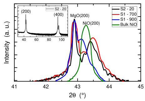
Thus, the measured (200) peak position shift indicates significant diffusion of Mg from the substrate into the layer activated by the high growth temperature, which would also explain the missing XRR oscillations as diffusion leads to a smeared-out density profile at the substrate-film interface. However, a thickness of about 40 nm still was measurable by the weak Pendellösung fringes in the scan around the (200) peak. Mg-diffusion into the layer is corroborated by the presence of a Mg-peak in SEM-EDX measurement for the S1-900 sample at an electron beam energy of only 2 keV, which excludes penetration into the MgO substrate.
Hence, epitaxial NiO(100) layers can be grown on MgO(100) at growth temperatures in the range of 20°C to 700°C, whereas a higher temperature of 900°C results in significant Mg incorporation from the substrate into the layer.
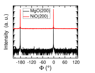
III.2 Epitaxial relationship
MgO(100) substrate
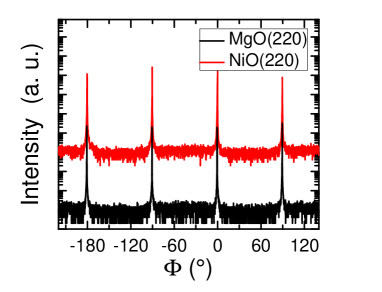
To determine the in-plane expitaxial relationship and the potential existence of rotational domains, XRD peaks of inclined lattice planes were measured by -scans with rotational angle around the surface normal. These measurements were performed in the skew-symmetric geometry with the sample tilted by the angle between the surface normal and the normal of the inclined lattice planes. Fig. 3 shows such a -scan of the NiO(220) and MgO(220) peak of sample S2-20. It indicates a fourfold rotational symmetry for substrate and layer, as expected for the (100)-oriented structure, confirming the absence of rotational domains in substrate and film. In addition, the peaks of the substrate are at the same positions as the layer peaks, indicating coinciding directions of substrate and layer. Therefore, the epitaxial relationship is cube-on-cube, i.e.:
This cube-on-cube growth is maintained under
all investigated growth conditions, including the growth with molecular
oxygen and that at high growth temperature with Mg-incorporation,
as confirmed by XRD characterization (not shown) of all samples.
Rocking curves (ω-scan) measured by XRD are normally used for quality investigations of thin layers. The full-width-at-half-maximum (FWHM) of the peak gives information about the crystal perfection, since it correlates with the range of tilt angles of the measured lattice planes. Higher FWHM can be created by defects, such as misfit dislocations,Moram and Vickers (2009) hence a smaller FWHM indicates a higher quality of the crystal. The FWHM can, however, also be affected by curvature or substrate quality. Indeed, MgO substrates often consist of multiple macroscopic domains with low-angle domain boundaries and a wide range of quality can occur even for the same vendor and batch.Schroeder et al. (2015) Depending on the size, tilt and occurence of those macroscopic domains, a MgO peak can consist of one or multiple features,Schroeder et al. (2015) which can be seen by closely inspecting the MgO(200) peak in Fig. 2 showing a sharp peak for S2-20 but multi-peak structure for S1-700 and S1-900. The FWHMs of the layers grown on MgO(100) are similar for most samples and around 0.05° to 0.07°. Only series two shows higher values (0.21 °-0.42 °) for all temperatures, except 20 °C.
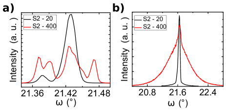
An example of the two different rocking curves is shown in Fig. 4. The broader peaks can be explained by the quality of the substrate which depends on the orientation of the different macroscopic domains it consists of. Due to the strong impact of the fluctuating substrate quality, no correlation between the quality of the layers and the temperature or oxygen flux influence can be extracted from the FWHM. However, the measured values can be considered as an upper bound estimate with low FWHM (<0.07°) on the higher quality substrates.
MgO(111) substrate
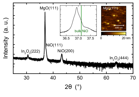
The scan of the layer grown on MgO(111)
is shown in Fig. 5. It indicates the presence
of a NiO(200) and a NiO(111) peak (seen as a shoulder at the high
angle-side of the MgO(111) peak from the substrate). The NiO(111)
peak can be clearly distinguished from the MgO(111) in the inset of
Fig. 5. Therefore, a single crystalline growth
on the MgO(111) substrate did not take place under our growth conditions,
likely related to a low surface quality of the substrate (see AFM
image in Fig. 5) with a RMS roughness of 2.3 nm,
that may trigger the formation of the thermodynamically stable (100)
surface. The higher stability of the {100}- compared to the {111}-
facet has been often observed by the growth of NiO tetrahedrons with
{100} planes on MgO(111) and Al2O3(0001) substrates.Warot et al. (2002b, a); Becker et al. (2017a)
Additionally, a weak indium oxide peak is visible which is due to
oxidized traces of indium that unintentionally covered small parts
of the surface during In-bonding of the substrate.
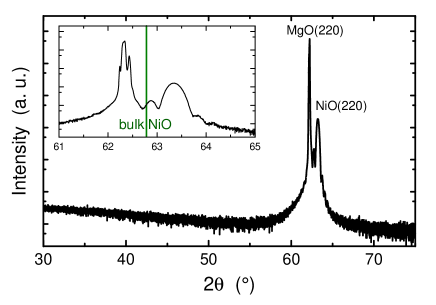
MgO(110) substrate
In the scan of the MgO(110) sample a NiO(220) peak is measured beside the substrate peak (see Fig. 6), indicating a single crystalline layer. For this layer the scan of the NiO(200) reflex is shown in Fig. 7. It shows a twofold symmetry, which is expected for the (110) surface orientation. In addition, the peaks of substrate and layer are at the same positions. Thus, the epitaxial relationship is cube-on-cube, i.e:
III.3 Oxygen-rich growth and oxygen stoichiometry of the layer
Generally, the growth rate of an oxide film can be limited by the metal flux, corresponding to O-rich growth conditions, or by the O-flux, corresponding to metal-rich growth conditions.Vogt and Bierwagen (2016) All films were grown at the same Ni cell temperature, resulting in an approximately constant Ni-flux. The measured growth rates ranging from 0.05 Å/s to 0.09 Å/s did not show a systematic dependence on the reactive O-flux, despite a strong variation of the oxidizing agent ranging from a low flux of 0.3 sccm molecular oxygen to a high flux of 1 sccm of plasma-activated oxygen. The growth rate rather decreased over time due to the gradual formation of NiO at the orfice of the Ni cell. Consequently, the growth was metal-flux limited, O-rich under all investigated growth conditions.
Under different growth conditions many stoichiometries of nickel oxide have been prepared by other growth techniques: Oxygen-rich stoichiometries of sputtered and electro-deposited Ni3O4, Ni2O3 and NiO2Murphy and Hutchins (1995) as well as ion-beam sputtered NixO ranging from slightly O-rich (x=0.9) to Ni-rich (x=1.45)Becker et al. (2017b) stoichiometries have been reported. Interestingly, XRD of the latter ones showed a cubic-NiO peak that was almost unchanged with stoichiometry.Becker et al. (2017b) XRD of all our layers indicates only the cubic phase by the presence of the NiO(200) and (400) peaks and the peak seen in the -scans. A small shift of the NiO(200) peak of S2-700 with respect to S1-700 is visible but is related rather to strain than to stoichiometry as the thickness of S1-700 and S2-700 is below and above the critical thickness of 60 nm, respectively.
To clarify the effect of the different oxygen fluxes during growth on the stoichiometry of our films further investigations by EDX were performed with the samples S1-250, S1-700, and S2-700. The results are shown in Tab. 2. Due to the accuracy of 1-2 % of the measurement both samples of S1 can be seen as stoichiometric NiO, whereas a small Ni excess of <5 At% was found in S2-700. This Ni excess would be consistent with the lower O-flux used in S2 and could manifest itself in the existence of Ni-interstitials or O-vacancies.
Hence, in our study both oxygen fluxes lead to nearly stoichiometric NiO films grown under O-rich conditions.
| [°C] | 250 | 700 | |
|---|---|---|---|
| S1 | At% O | 49.9 | 49.3 |
| At% Ni | 50.1 | 50.7 | |
| [°C] | 700 | ||
| S2 | At% O | 47.2 | |
| At% Ni | 52.8 |
III.4 Surface morphology and annealing
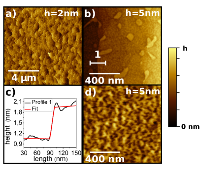
The morphology of all samples on MgO(100) was investigated by AFM. The clean MgO substrate is shown in Fig. 8 a). The surface is flat and has a root-mean-squared (RMS) roughness of about 0.1 nm. Furthermore, AFM images of S2-20, S1-700 and S2-700 are also shown in Fig. 8(b), (c) and (d), respectively. All layers show a surface consisting of grains, independent of temperature and oxygen flux. As it is shown in Tab. 3, a correlation between growth temperature and grain size can be seen. Overall, the sizes of series two are bigger, indicating a higher adatom surface diffusion length consistent with the lower O-flux and a higher temperature. In addition, the table shows the RMS roughness of all samples. However, no clear relation between the temperature and the roughness can be found. Solely, the roughness of S1-900 (with Mg incorporated from the substrate) of 3.7 nm is significantly higher than that of NiO grown at lower temperature, although the average grain size is still around 50 nm (see Fig. 8 e).
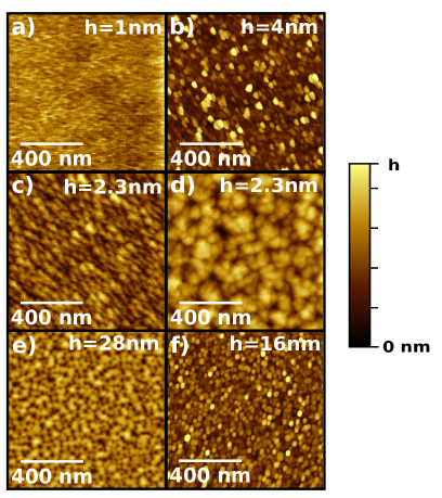
The layer grown with molecular oxygen (RF plasma power 0 W) also shows a higher roughness of about 2.5 nm due to the formation of tall islands (Fig. 8 f). This indicates a low surface diffusion length even at 700 °C, presumably due to the reduced adatom surface diffusion length by the lower oxidation power of molecular oxygen. This is in agreement with the investigation by Peacor et al. who observed NiO island formation for growth with molecular oxygen and smoother surfaces for samples grown with the more reactive NO2.Peacor and Hibma (1994) For growth temperatures higher than 400 °C even unoxidized nickel has been observed in O2 grown layers. Peacor et al. further indicate a correlation of the small grain size with a low surface diffusion rate for temperatures under 300 °C and insufficient oxidation power of O2 at temperatures above 400 °C.
Thus, the combination of a high temperature and a low flux (large surface diffusion length), together with a high oxidation power (f. e. NO2 or plasma-activated O2) is required to growth smooth NiO layers.
| Tg[°C] | 250 | 450 | 700 | 900 | ||
|---|---|---|---|---|---|---|
| S1 | RRMS[nm] | 0.7 | 0.1 | 0.3 | 3.7 | |
| size [nm] | 30 | 15 | 50 | 67 | ||
| Tg[°C] | 20 | 200 | 400 | 700 | ||
| S2 | RRMS[nm] | 0.7 | 0.25 | 1.6 | 0.4 | |
| size [nm] | 40 | 40 | 20 | 80 |
To further improve the surface morphology, different annealings
were tested to create a stepped layer surface. On the one hand, annealing
after growth of the NiO layer and, on the other hand, annealing before
growth of the MgO surface was investigated. Annealing in a tube furnace
after growth as suggested by Ohta et al. Ohta et al. (2003) led to the
disappearance of the NiO peaks in all XRD measurements (not shown
here). We used an annealing temperature of 1200 °C for
30 min in air.
The influence of annealing on the surface morphology of MgO has already
been investigated by Ahmed et al., who found terraces after 3 hours
at 1200 °C in an oxygen atmosphere.Ahmed et al. (1996)
In our study, a stepped surface (see Fig. 9 a))
was reached after annealing the substrate four hours at 1150 °C
in a tube furnace with oxygen. Fig 9 b) is a
magnified image of a) and shows the around 1 µm wide steps.
On the steps small islands formed possibly due to a small diffusion
length. The step height is around 0.9 nm (see profile line in Fig. 9 c))
which is similar to the expected height of 0.84 nm for a MgO double
step. After the growth of NiO (700 °C, 0.3 sccm) on this
substrate, no steps are visible (see Fig. 9 d)).
Compared to Fig. 8 b) the morphology of the
layer changed according to the formation of interconnected islands
instead of grains. However, the steps are not adopted as shown in
Fig. 9 d). The roughness for the NiO layer on
the annealed MgO is 0.4 nm, which is similar to the sample roughness
of S1-700 and S2-700 (see Tab. 3). No difference
was seen in the XRD scan, either. Further improvement of the annealing
conditions for more defined steps without islands could lead to a
flat surface morphology without grains and improve the NiO layer.
This could be achieved by off-cut substrates with a terrace
width for example of less than 80 nm for the S2-700 growth corresponding
to an off-cut angle above 0.3°.
III.5 Raman quality metrics of NiO(100)/MgO(100)
For rock-salt structures Raman spectroscopy is able to provide information about the crystal quality as the first-order scattering by optical phonons is forbidden due to the symmetry selection rules.Dietz et al. (1971); Mironova-Ulmane et al. (2007) Crystal imperfections or the distortion below the Néel temperature (TN) could lead to the occurence of a first-order optical phonon line (1P) in Raman spectra. However, Dietz et al.Dietz et al. (1971) showed no significant increase of the 1P peak for temperatures below TN. Thus, the intensity of 1P Raman peak still correlates with the layer quality. Since second-order Raman scattering by optical phonons (2P) is allowed also for perfect crystals, the intensity of the first-order Raman peak (I1P) normalized to that of the second-order peak (I2P) can be utilized as an inverse figure of merit for the crystal quality ():
| (1) |
where I1P and I2P are the integrated intensities of the corresponding Raman peaks. Since I1P = 0 ( = 0) for a perfect crystal, the value of increases with the density of crystal defects.
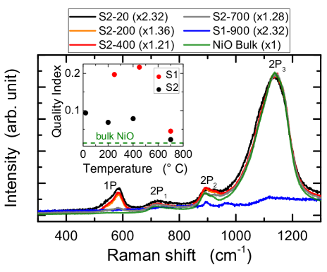
For NiO three 2P peaks are visible in figure 10.
The corresponding modes have been identified as the 2TO modes (2P1),
the TO+LO modes (2P2), and the 2LO modes (2P3) by Mironova-Ulmane
et al.Mironova-Ulmane et al. (2007) For our calculation of we used I2P
as the integrated intensity of the 2P3 peak. Raman spectra of
sample series 2 are shown in Fig. 10 with the intensity
normalized to the intensity of 2P3. The decrease of the first-order
Raman peak (1P) clearly reveals the improvement of the NiO crystal
quality with increasing growth temperature. The NiO-MgO alloy (S1-900)
shows no defined Raman peak. The crystal quality index defined
in Eq. 1 is shown in the inset in Fig. 10
for all NiO films grown on MgO(100) as a function of growth temperature.
For both sample series (S1 and S2), approaches at high temperature
the value of the nearly perfect bulk NiO reference sample (shown as
dashed line in the inset in Fig. 10). The observed
improvement of the crystal quality with increasing growth temperature
is a frequently observed phenomenon for MBE grown films. The reason
for this improvement is given by enhanced diffusion length of adatoms
on the growth surface which increases the probability for the occurence
of step flow growth and the the formation of a thermodynamically stable
structure.Arthur (2002) Consequently, the density of crystal
defects becomes reduced at elevated growth temperatures, especially
when the lattice mismatch between film and substrate is small. The
generally smaller values (better crystal quality) observed for
sample series two (see inset in Fig. 10) can be
explained by the smaller oxygen flux during growth. The lower surface
coverage by oxygen atoms also enables a higher surface mobility of
adatoms which is beneficial for the obtained crystal quality (as explained
above). Furthermore, the higher crystal quality of NiO films prepared
with smaller oxygen flux indicates that oxygen vacancies are not the
main source of the crystal imperfections in the investigated NiO films.
Our results demonstrate that Raman spectroscopy can be utilized in
a very efficient manner to evaluate the crystal quality of NiO films.
A similar approach has already been used to estimate the amount of
crystal defects in SrTiO3 films.Tenne et al. (2007) In contrast to
the XRD measurements, Raman spectroscopy is sensitive to imperfections
of the crystal structure in the investigated NiO films since the Raman
selection rules are influenced by the local crystal symmetry rather
than by the flatness of the substrate. The local symmetry, however,
is only influenced by lattice distortions and defects or grain boundaries.
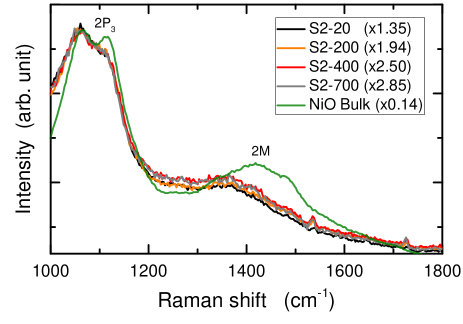
Regarding the magnetic ordering, we investigated second-order
magnon scattering using a 405-nm diode laser for excitation
since the corresponding two magnon (2M) peak could not be observed
for excitation at 325 nm.Aytan et al. (2017) The 2M peak
is in general observable below the Néel temperature as a signature
of antiferromagnetic ordering. Based on a detailed investigation of
the dispersion for different directions in NiO, Betto et al.Betto et al. (2017)
revealed a reduction of the leading superexchange parameter for films
compared to bulk NiO, presumably due to strain. For our films, independent
of the growth temperature, a 2M peak is measurable as a fingerprint
of antiferromagnetic ordering (see Fig. 11). The
observed redshift with respect to bulk NiO reflects the expected strain-induced
decrease in the superexchange parameter,Betto et al. (2017) which is proportional
to the 2M frequency.Gandhi et al. (2011)
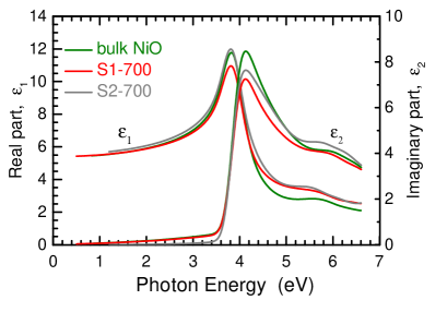
III.6 Optical properties
The optical properties are investigated by ellipsometry measurements of the NiO films on MgO(100) substrates. For the evaluation of the data, a three-layer model was used: Two NiO layers on a MgO substrate. The topmost NiO layer is needed to describe the surface roughness of the NiO and the other one describes the actual NiO film properties. The roughness layer was modeled by the Bruggeman effective medium approach assuming 50 % voids. It has a thickness of 2-7 nm. In most of the actual NiO layers voids were needed as well for the description of the optical properties, however only to a volume fraction below 7 %. There is a trend visible that less voids have to be assumed for higher growth temperatures, which indicates a better crystal quality. For the S2 samples an introduction of a certain inhomogeneity, that could be related to thickness fluctuation on the sample, was found to produce a better fit than a model solely based on voids and surface roughness. However, the model properties inhomogeneity, voids, and surface roughness are intertwined inextricably.Aspnes et al. (1979); Ohlídal et al. (2017) The relative differences of surface roughness as found by AFM (Tab. 3) presently is not reflected by the roughness layer thickness dR (Tab. 4), determined by ellipsometry measurements. If however, the inhomogeneity would be removed from the model, the value for would follow more closely the trends found by AFM at the expense of a slightly decreased quality of the overall agreement between optical model and experimental data. All results are tabulated in table 4.
| Tg[°C] | 250 | 450 | 700 | ||
|---|---|---|---|---|---|
| S1 | dR [nm] | 7.3 | 4.5 | 7.0 | |
| dNiO [nm] | 47.3 | 23.1 | 41.4 | ||
| voids [%] | 7.2 | 0.0 | 3.4 | ||
| Tg[°C] | 20 | 200 | 400 | 700 | |
| dR [nm] | 4.0 | 4.0 | 7.0 | 2.0 | |
| S2 | dNiO [nm] | 61.2 | 60.4 | 53.1 | 60.7 |
| voids [%] | 7.3 | 4.5 | 4.6 | 3.7 | |
| I [%] | 7 | 17 | 31 | 13 |
The combined modeled thickness of the two NiO layers is similar to the thicknesses measured by XRR. Furthermore, all layers showed an onset of strong interband absorption around 3.6 eV, which is in excellent agreement with earlier experimental findings.Kang et al. (2007); Rödl and Bechstedt (2012); Ghosh et al. (2015); Battiato et al. (2016) All samples yield spectra with sharp and pronounced absorption features in the imaginary parts of their DFs which is a hint towards high crystalline and morphological quality. The DFs of the bulk NiO crystal and samples S1-700 and S2-700 are displayed in Fig. 12. The increasing value of the real part of the DF for the oxygen poor sample (S2-700) in the transparency region below about 3.5eV is in agreement with Ref. [(14)], however the general line shape and energy positions of distinguished features is in very good agreement to those of Refs. [(46; 47; 48; 49)]. The influence of different nickel oxide compositions (NixO) for example on the refractive index has been investigated by Becker et al. for x ranging from 0.9 to 1.45.Becker et al. (2017b)
III.7 Electrical properties
The idcs used in this study, reduced the measured resistance with respect to the sheet resistance by a defined geometry factor of for the structures shown in Fig. 13 a) and by a factor of using the structures shown in Ref [(50)]. Based on the measured resistance of the idcs, the calculated sheet resistances at room temperature for all samples grown on MgO(100) are higher than , indicating no significant bulk conductivity. The low bulk conductivity may be due to a too low concentration of unintentional acceptors (e.g. Ni vacancies) or the existence of a high concentration of compensating unintentional donors. Due to the high resistance of all samples any attempt to determine the conductivity type by Hall, capacitance-voltage or Seebeck measurements, failed.
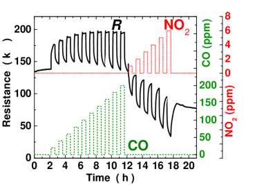
As an alternative for determining the conductivity type we measured the resistance change of the idcs upon exposure to reducing or oxidizing gases at elevated temperatures — a behavior that is exploited in oxide-semiconductor based gas sensors. Oxidizing gases, such as NO2, act as surface acceptors, whereas reducing gases, such as CO, act as surface donors.Kim and Lee (2014) Consequently, exposure to oxidizing gases would reduce the number of electrons in -type oxides and thus increase their resistance, whereas it would increase the number of holes and hence decrease the resistance of -type oxides.Barsan et al. (2010); Kim and Lee (2014) The effect of reducing gases is opposite to that of oxidizing gases by either acting directly as surface donors or by reacting with and thus reducing the number of adsorbed surface-accepting oxygen.Barsan et al. (2010) Fig. 13 (b) shows the resistance of the idcs (a) for S2-400 as a function of NO2 and CO content in synthetic air without humidity. The increasing resistance under CO exposure and decreasing resistance under NO2 exposure consistently demonstrates -type conductivity of our NiO sample.
IV Summary and conclusions
We investigated the growth of NiO layers by plasma-assisted MBE on MgO(100), MgO(110) and MgO(111). On MgO(100) and MgO(110) the NiO layers were single crystalline with (100) and (110) orientation, respectively, having an epitaxial cube-on-cube relationship to the substrate. The NiO layer on MgO(111), in contrast, consisted of (111) and (001) oriented domains, likely related to the rough substrate surface. The influence of growth conditions on film properties was investigated on MgO(100) by the variation of growth temperature and active oxygen flux: Single crystalline growth was maintained on MgO(100) in the entire range of investigated growth temperatures, i.e. from 20 °C to 900 °C, and different oxygen fluxes (including molecular oxygen), that all resulted in O-rich and Ni-limited growth conditions. Layers grown under vastly different conditions were fairly stoichiometric with an oxygen content in the range of 47 at.% to 50 at.%. All layers were transparent to the visible light and had a RMS surface roughness typically below 1 nm. Only the growth at 900° C or with molecular oxygen led to significantly higher roughnesses. At the growth temperature of 900 °C Mg diffused from the substrate into the layer, resulting in a MgxNi1-xO(100) film.
The intensity ratios of quasi-forbidden one-phonon to allowed two-phonon Raman peaks was introduced as a new quality metrics, which indicated the highest layer quality for a high growth temperature of 700 °C and a low oxygen flux.
Therefore, for optimum crystal quality a growth of NiO on MgO(100) at a temperature °C but °C using a low, plasma-activated oxygen flux is recommended by our data. A comparison to available literature suggests the importance of a low growth rate. A further improvement in crystal quality by using higher growth temperatures may be enabled by a thermodynamically more stable substrate material, such as sapphire (Al2O3), that does not diffuse into the growing film. The epitaxy by ion-beam sputtering on a- and c-plane Al2O3 resulted in NiO(111) films with two rotational domains, whereas that on m-plane Al2O3 resulted in NiO(110) films consisting of multiple tilt domains.Becker et al. (2017a) Preparation of atomically bistepped (step heigth 0.433 nm) c-plane Al2O3 surfaces by annealing prior to growth has been shown to prevent the formation of rotational domains, enabling the growth of single crystalline NiO(111) films thereon as demonstrated by pulsed laser deposition.Yamauchi et al. (2015)
AFM images of our films showed a surface composed of grains with larger size for higher temperatures or lower activated oxygen flux, indicating an increasing surface diffusion length. Together with the Raman-derived quality metrics a correlation between a high layer quality and a high surface diffusion length is found.
All grown layers were semi-insulating with sheet resistance G, indicating a too low concentration of unintentional acceptors (e.g. Ni vacancies) or the existence of a sufficiently high concentration of compensating unintentional donors. Nevertheless, p-type conductivity was confirmed at elevated temperature by gas response measurements of a representative layer, demonstrating the suitability of single crystalline NiO thin films for fundamental gas sensor research.
Acknowledgements.
We would like to thank S. Rauwerdink and W. Seidel for cleanroom processing, H.-P. Schönherr for MBE support, U. Jahn for measuring and evaluating the EDX data, and J. M. J. Lopes for critically reading the manuscript.. This work was performed in the framework of GraFOx, a Leibniz-ScienceCampus partially funded by the Leibniz association. M. B., P. F., and J. F. gratefully acknowledges financial support by the Leibniz Association.References
- Ohta et al. [2003] H. Ohta, M. Kamiya, T. Kamiya, M. Hirano, and H. Hosono, Thin Solid Films, 445 (2003). doi: 10.1016/S0040-6090(03)01178-7.
- Rao and Smakula [1965] K. V. Rao and A. Smakula, J. Appl. Phys., 36(6), 2031 (1965). doi: 10.1063/1.1714397.
- Zhang et al. [2018] J.-Y. Zhang, W. Li, R. L. Z. Hoye, J. MacManus-Driscoll, M. Budde, O. Bierwagen, L. Wang, Y. Du, M. Wahila, L. F. J. Piper, T.-L. Lee, H. Edwards, V. R. Dhanak, and H. Zhang, J. Mater. Chem. C, 6, 2275–2282 (2018). doi: 10.1039/C7TC05331B.
- Schuler et al. [2005] T. M. Schuler, D. L. Ederer, and S. Itza-Oritz, Phys. Rev. B, 71(115113), 1 (2005). doi: 10.1103/PhysRevB.71.115113.
- Massidda et al. [1999] S. Massidda, M. Posternak, A. Baldereschi, and R. Resta, Phys. Rev. Lett., 82(2), 430 (1999). doi: 10.1103/PhysRevLett.82.430.
- Hoshiya et al. [1994] H. Hoshiya, M. Komuro, K. Mitsuoka, and Y. Sugita, IEEE Transl. J. Magn. Jpn., 9(6), 236 (1994). doi: 10.1109/TJMJ.1994.4565986.
- Becker et al. [2017a] M. Becker, A. Polity, and P. J. Klar, Journal of Applied Physics, 122(17), 175303 (2017). doi: 10.1063/1.4991601. URL https://doi.org/10.1063/1.4991601.
- Kim and Lee [2014] H.-J. Kim and J.-H. Lee, Sens. Actuators, B, 192, 607 (2014). doi: http://dx.doi.org/10.1016/j.snb.2013.11.005.
- Miller et al. [2014] D. R. Miller, S. A. Akbar, and P. A. Morris, Sens. Actuators B, 204, 250 (2014). doi: 10.1016/j.snb.2014.07.074.
- Zhang et al. [2016] K. H. L. Zhang, K. Xi, M. G. Blamire, and R. G. Egdell, J. Phys. Condens. Matter, 28(38), 1 (2016). doi: 10.1088/0953-8984/28/38/383002.
- von Wenckstern et al. [2015] H. von Wenckstern, D. Splith, S. Lanzinger, F. Schmidt, S. MÃŒller, P. Schlupp, R. Karsthof, and M. Grundmann, Adv. Electron. Mater., 1, 1400026 (2015). doi: 10.1002/aelm.201400026.
- Irwin et al. [2007] M. D. Irwin, D. B. Buchholz, A. W. Hains, R. P. H. Chang, and T. J. Marks, Proc. Natl. Acad. Sci. U.S.A, 105(8), 2783 (2007). doi: 10.1073/pnas.0711990105.
- Warot et al. [2001a] B. Warot, E. Snoeck, P. Baulès, J. C. Ousset, M. J. Casanove, S. Dubourg, and J. F. Bobo, Appl. Surf. Sci., 177(4), 287 (2001). doi: 10.1016/S0169-4332(01)00223-9.
- Becker et al. [2017b] M. Becker, F. Michel A. Polity, and P. J. Klar, Phys. Status Solidi B, 255(1700463) (2017). doi: 10.1002/pssb.201700463.
- Murphy and Hutchins [1995] T. P. Murphy and M. G. Hutchins, Sol. Energy Mater. Sol. Cells, 39(2-4), 377 (1995). doi: 10.1016/0927-0248(96)80003-1.
- Peacor and Hibma [1994] S. D. Peacor and T. Hibma, Surf. Sci., 301, 11 (1994). doi: 10.1016/0039-6028(94)91283-1.
- Tachiki et al. [2000] M. Tachiki, T. Hosomi, and T. Kobayashi, Jpn. J. Appl. Phys., 39 Part 1(4A), 1817 (2000). doi: 10.1143/JJAP.39.1817.
- Manders et al. [2013] J. R. Manders, S.-W. Tsang, M. J. Hartel, T.-H. Lai, S. Chen, C. M. Amb, J. R. Reynolds, and F. So, Adv. Funct. Mater, 23(23), 2993 (2013). doi: 10.1002/adfm.201202269.
- Lind et al. [1992] D. M. Lind, S. D. Berry, G. Chem, H. Mathias, and L. R. Testardi, Phys. Rev. B, 45(4), 1838 (1992). doi: 10.1103/PhysRevB.45.1838.
- Mares et al. [2010] J. W. Mares, R. C. Boutwell, M. Wei, A. Scheurer, and W. V. Schoenfeld, Appl. Phys. Lett., 97, 161113 (2010). doi: 10.1063/1.3503634.
- Rombach et al. [2016] J. Rombach, A. Papadogianni, M. Mischo, V. Cimalla, L. Kirste, O. Ambacher, T. Berthold, S. Krischok, M. Himmerlich, S. Selve, and O. Bierwagen, Sensors and Actuators B: Chemical, 236, 909 (2016). ISSN 0925-4005. doi: 10.1016/j.snb.2016.03.079.
- Wang et al. [2011] H. Wang, G. Fang, H. Long, S. Li, X. Mo, H. Huang, H. Zhou, and X. Zhao, Semicond. Sci. Technol., 26, 125015 (2011). doi: 10.1088/0268-1242/26/12/125015.
- Warot et al. [2002a] B. Warot, E. Snoeck, P. Baulès, J. C. Ousset, M. J. Casanove, S. Dubord, and J. F. Bobo, J. Cryst Growth., 234(4), 704 (2002). doi: 10.1016/S0022-0248(01)01767-5.
- Warot et al. [2001b] B. Warot, E. Snoeck, P. Baulès, J. C. Ousset, M. J. Casanove, S. Dubourg, and J. F. Bobo, J. Cryst Growth., 224(3-4), 309 (2001). doi: 10.1016/S0022-0248(01)01017-X.
- Warot et al. [2002b] B. Warot, E. Snoeck, J. C. Ousset, M. J. Casanove, S. Dubord, and J. F. Bobo, Appl. Surf. Sci., 188(1-2), 151 (2002). doi: 10.1016/S0169-4332(01)00725-5.
- Goldhahn [2003] R. Goldhahn, Acta Phys. Pol A, 104, 123 (2003). doi: 10.12693/APhysPolA.104.123.
- Bruggeman [1935] D. A. G. Bruggeman, Ann. Phys. (Berl.), 416(7), 636 (1935). doi: 10.1002/andp.19354160705.
- Feneberg et al. [2016] M. Feneberg, J. Nixdorf, C. Lidig, R. Goldhahn, Z. Galazka, O. Bierwagen, and J. S. Speck, Phys. Rev. B, 93(4), 045203 (2016). doi: 10.1103/PhysRevB.93.045203.
- Barsan et al. [2010] N. Barsan, C. Simion, T. Heine, S. Pokhrel, and U. Weimar, J. Electroceramics, 25(1), 11 (2010). doi: 10.1007/s10832-009-9583-x.
- Fewster [1999] P. F. Fewster, Rep. Prog. Phys., 59, 1339 (1999). doi: 10.1088/0034-4885/59/11/001.
- James and Hibma [1999] M. A. James and T. Hibma, Surf. Sci., 433, 718 (1999). doi: 10.1016/S0039-6028(99)00476-8.
- Boutwell et al. [2012] R. C. Boutwell, M. Wei, A. Scheurer, J. W. Mares, and W. V. Schoenfeld, Thin Solid Films, 520(13), 4302 (2012). doi: 10.1016/j.tsf.2012.02.065.
- Moram and Vickers [2009] M. A. Moram and M. E. Vickers, Rep. Prog. Phys., 72(3), 1 (2009). doi: 10.1088/0034-4885/72/3/036502.
- Schroeder et al. [2015] J.L. Schroeder, A.S. Ingason, J. Rosén, and J. Birch Thin, J. Cryst Growth., 420, 22 (2015). doi: 10.1016/j.jcrysgro.2015.03.010.
- Vogt and Bierwagen [2016] P. Vogt and O. Bierwagen, Appl. Phys. Lett., 109, 062103 (2016). doi: http://dx.doi.org/10.1063/1.4960633.
- Ahmed et al. [1996] F. Ahmed, K. Sakai, H. Ota, R. Aoki, N. Ikemiya, and S. Hara, J. Low Temp. Phys., 105, 1343 (1996). doi: 10.1007/BF00753887.
- Dietz et al. [1971] R. E. Dietz, G. I. Parisot, and A. E. Meixner, Phys. Rev. B, 4(7), 2302 (1971). doi: 10.1103/PhysRevB.4.2302.
- Mironova-Ulmane et al. [2007] N. Mironova-Ulmane, A. Kuzmin, I. Steins, J. Grabis, I. Sildos, and M. Pärs, J. Phys. Conf. Ser., 93(012039) (2007). doi: 10.1088/1742-6596/93/1/012039.
- Arthur [2002] J. R. Arthur, Surf. Sci., 500, 189 (2002). doi: 10.1016/S0039-6028(01)01525-4.
- Tenne et al. [2007] D. A. Tenne, I. E. Gonenli, A. Soukiassian, D. G. Schlom, S. M. Nakhmanson, K. M. Rabe, and X. X. Xi, Phys. Rev. B, 76(2), 024303 (2007). doi: 10.1103/PhysRevB.76.024303.
- Aytan et al. [2017] E. Aytan, B. Debnath, F. Kargar, Y. Barlas, M. M. Lacerda, J. X. Li, R. K. Lake, J. Shi, and A. A. Balandin, Appl. Phys. Lett., 111(25) (2017). doi: 10.1063/1.5009598.
- Betto et al. [2017] D. Betto, Y. Y. Peng, S. B. Porter, G. Berti, A. Calloni, G. Ghiringhelli, and N. B. Brookes, Phys. Rev. B, 96(2) (2017). doi: 10.1103/PhysRevB.96.020409.
- Gandhi et al. [2011] A. C. Gandhi, C.-Y. Huang, C. C. Yang, T. S. Chan, C.-L. Cheng, Y.-R. Ma, and S. Y. Wu, Nanoscale Res. Lett., 6, 485 (2011). doi: 10.1186/1556-276X-6-485.
- Aspnes et al. [1979] D. E. Aspnes, J. B. Theeten, and F. Hottier, Phys. Rev. B, 20(8), 3292 (1979). doi: 10.1103/PhysRevB.20.3292.
- Ohlídal et al. [2017] I. Ohlídal, D. Franta, and D. Necas, Appl. Surf. Sci., 421, 687 (2017). doi: 10.1016/j.apsusc.2016.10.186.
- Kang et al. [2007] T. D. Kang, H. S. Lee, and H. Lee, J. Korean Phys. Soc., 50(3), 632 (2007). doi: 10.3938/jkps.50.632.
- Rödl and Bechstedt [2012] C. Rödl and F. Bechstedt, Phys. Rev. B, 86(23), 235122 (2012). doi: 10.1103/PhysRevB.86.235122.
- Ghosh et al. [2015] A. Ghosh, C. M. Nelson, L. C. Abdallah, and S. Zollner, J. Vac. Sci. Technol. A, 33(6), 061203 (2015). doi: 10.1116/1.4932514.
- Battiato et al. [2016] S. Battiato, M. M. Giangregorio, M. R. Catalano, R. Lo Nigro M. Losurdo, and G. Malandrino, RSC Adv., 6(37), 30813 (2016). doi: 10.1039/C6RA05510A.
- Kaspar et al. [2016] T. C. Kaspar, P. V. Sushko, M. E. Bowden S. M. Heald, A. Papadogianni, C. Tschammer, O. Bierwagen, and S. A. Chambers, Phys. Rev. B, 94, 155409 (2016). doi: 10.1103/PhysRevB.94.155409.
- Yamauchi et al. [2015] R. Yamauchi, Y. Hamasaki, T. Shibuya, A. Saito, N. Tsuchimine, K. Koyama, A. Matsuda, and M. Yoshimoto, Sci. Rep, 5, 14385 (2015). doi: 10.1038/srep14385.