Novel Wake-up Scheme for Energy-Efficient Low-Latency Mobile Devices in 5G Networks
Abstract
Improved mobile device battery lifetime and latency minimization are critical requirements for enhancing the mobile broadband services and user experience. Long-term evolution (LTE) networks have adopted discontinuous reception (DRX) as the baseline solution for prolonged battery lifetime. However, in every DRX cycle, the mobile device baseband processing unit monitors and decodes the control signaling, and thus all instances without any actual data allocation leads to unnecessary energy consumption. This fact together with the long start-up and power-down times can prevent adopting frequent wake-up instants, which in turn leads to considerable latency. In this work, a novel wake-up scheme is described and studied, to tackle the trade-off between latency and battery lifetime in future G networks, seeking thus to facilitate an always-available experience, rather than always-on. Analytical and simulation-based results show that the proposed scheme is a promising approach to control the user plane latency and energy consumption, when the device is operating in the power saving mode. The aim of this article is to describe the overall wake-up system operating principle and the associated signaling methods, receiver processing solutions and essential implementation aspects. Additionally, the advantages compared to DRX-based systems are shown and demonstrated, through the analysis of the system energy-efficiency and latency characteristics, with special emphasis on future 5G-grade mobile devices.
Index Terms:
G, mobile device, energy consumption, detection, latency, DRX, wake-up receiver, wake-up signaling.1 Introduction
In future G networks, it is expected that a diverse set of services, e.g., augmented and virtual reality, cloud gaming, ultra-high-definition video streaming and connected cars, with very aggressive quality-of-service (QoS) requirements will become ubiquitous [2]. For instance, in order to avoid virtual reality sickness as a result of using superimposed computer-generated content over live images viewed through smartphone cameras, acceptable end-to-end latency is less than a few tens of milliseconds, and requires throughput in the order of Mbps [3]. On the other hand, the slow technological progress in battery capacities complicates adopting more and more complex and high-rate continuous processing in the devices, and therefore different energy saving features and mechanisms are of substantial importance [4]. To this end, multiple experimental investigations show that the most energy consuming components of smartphones can be attributed to the cellular connectivity subsystem and the display [5, 6, 7]. Therefore, the design of an energy-efficient cellular subsystem, utilizing the battery energy capacity in an efficient manner, is extremely paramount. In this article, due to the asymmetric data traffic which is dominated by downlink [8], our main focus is on the device receive mode.
Since the last decade, different mobile device energy saving features have been considered by different standardization and device implementation bodies. Particularly, the rd generation partnership project (GPP) has introduced discontinuous reception (DRX) as an important energy saving mechanism for long-term evolution (LTE) mobile networks [9]. DRX enables the mobile device to reduce energy consumption by systematically turning some components of the cellular subsystem in sleep mode for certain periods of time. On the other hand, for low communication latencies, it is necessary to shorten the DRX cycle as much as possible, emulating an always-available experience. However, due to the existence of relatively long start-up and power-down periods, as well as high energy consumption of the baseband processing unit (BBU) during the active time, the DRX mechanism cannot alone boost the G mobile devices battery lifetime sufficiently, especially when reduced latencies with good power-efficiency are pursued.
In general, the above limitations prevent designing and facilitating energy-efficient low-latency communications in future G networks based on current DRX-based power saving mechanisms alone. In recent years, a new type of approach, the so-called wake-up receiver (WRx) concept, has been introduced to improve the lifetime of the nodes in wireless sensor networks (WSNs) [10]. In this article, the concept of WRx and associated wake-up signaling are utilized and developed to prolong the mobile devices battery lifetime while still facilitating controlled latency. We refer to the proposed WRx-empowered cellular subsystem as the new modem (NM) in the rest of this article. The extensive numerical results presented in the article show that the NM concept reduces the energy consumption of DRX-enabled cellular subsystem up to %, depending on the traffic pattern and user requirements, while guaranteeing a predictable and consistent latency in the order of milliseconds. Because of low complexity and low power consumption of the WRx, together with the relatively low latency, the developed NM approach is not only applicable for enhanced mobile broadband (eMBB) purposes, but also for machine-centric use cases, such as utility management, or potentially also for real-time command and control for remote medication and surgery, in which battery lifetime is critically important, while at the same time demanding low latency communication [3, 4].
The work reported in this article consists of developing a novel wake-up scheme for scheduled frame-based cellular radio systems, including the necessary wake-up signaling and detection processing, analyzing the achievable performance in terms of energy-efficiency and latency, as well as shortly addressing the needed processing integration into available LTE-optimized nm CMOS-based transceiver ICs. Specifically, building on our initial work in [1], the major contributions of this article can be stated as follows
-
•
an efficient wake-up signaling structure is introduced, where different orthogonal sequences are utilized to distinguish among different WRxs;
-
•
a low-complexity WRx processing solution is developed and analyzed to detect the corresponding sequence, and to acquire the associated time and frequency synchronization;
-
•
average latency and power consumption of the proposed concept are quantified and characterized in an analytical manner using semi-markov process;
-
•
extensive link- and system-level simulations are presented to quantify the correctness and effectiveness of the proposed scheme and analytical results, and to compare its performance with more ordinary DRX-based cellular subsystem.
To the best of authors’ knowledge, this work is in the fore-front in developing such a wake-up based scheme for G mobile devices, such that all relevant aspects covering the wake-up signal structure, detection processing, energy-consumption and latency analysis, implementation details and the achievable overall system performance are all systematically addressed. Overall, the proposed scheme and the article should be of interest to a broad readership including academic and industrial research communities, who are seeking feasible methods to reduce the energy consumption of mobile devices.
The mathematical notations used in this work are as follows: represents the identity matrix, represent conjugate operation, denotes a parameter estimate, denotes the transpose operation, is the expectation operation, is the probability of occurrence, and represents the floor function. For readers’ convenience, the most essential variables used throughout the paper are listed in Table I. Furthermore, a list of key abbreviations and acronyms used in this paper can be found in Table II.
| Variable | Definition | |||||
|---|---|---|---|---|---|---|
| start-up time of cellular module | ||||||
| power-down time of cellular module | ||||||
| synchronization time of cellular module | ||||||
| power consumption of cellular subsystem at sleep state | ||||||
| power consumption of cellular subsystem at active state | ||||||
| wake-up cycle | ||||||
| monitoring duration of WRx per w-cycle | ||||||
| sleep period of WRx per w-cycle | ||||||
| time offset of wake-up scheme | ||||||
| on-time duration | ||||||
| inactivity timer | ||||||
| wake-up timer | ||||||
| probability of false alarm | ||||||
| probability of misdetection | ||||||
| the cyclic-prefix length of the OFDM symbol in terms of samples | ||||||
| the number of samples of body of OFDM symbol | ||||||
| the overall number of guard subcarriers around of each PDWCH group | ||||||
| length of Zadoff-Chu sequence | ||||||
| number of mobile devices within PDWCH group | ||||||
| size of FFT | ||||||
| wake-up indicator of mobile device | ||||||
| cyclic-shift of mobile device | ||||||
| DFT of root ZC sequence with cyclic-shift of | ||||||
| -point FFT output of OFDM symbol | ||||||
| fractional carrier frequency offset | ||||||
| integer carrier frequency offset | ||||||
| integer-valued OFDM symbol’s STO in terms of sampling instant time | ||||||
| index of OFDM symbol carrying PDWCH | ||||||
|
||||||
|
||||||
| PDP of the received signal at OFDM symbol | ||||||
|
||||||
|
||||||
| session inter-arrival time | ||||||
| packet call inter-arrival time within the session | ||||||
| packet inter-arrival time within the packet call | ||||||
| the power state of NM | ||||||
| steady state probability that NM is at | ||||||
| transition probability from to | ||||||
| holding times for |
| Abbreviation/Acronym | Definition | |||
| ASIC | application-specific integrated circuit | |||
| BBU | baseband processing unit | |||
| CFO/STO | carrier frequency/symbol time offset | |||
| DRX | discontinuous reception | |||
| gNB | 5G base-station | |||
| LTE | long-term evolution | |||
| LPO/HPO | low/high-power low/high-precision electronic oscillator | |||
| NM | new modem | |||
| PDP | power delay profile | |||
| PDCCH/PDSCH | physical downlink control/shared channel | |||
| PDWCH | physical downlink wake-up channel | |||
| RFIC | radio frequency integrated circuit | |||
| UE | user equipment | |||
| WRx | wake-up receiver | |||
| WSN | wireless sensor network | |||
| WI | wake-up indicator | |||
| w-cycle | wake-up cycle | |||
| ZC | zadoff-chu |
The rest of this article is organized as follows. Section 2 provides the problem description and motivation to solve it. Section 3 summarizes the current state of wake-up schemes available in literature. Section 4 introduces and describes the proposed novel wake-up scheme.The proposed solutions for WRx detection and synchronization processing are formulated in Section 5. Section 6 analyzes the average latency and power consumption of the proposed wake-up scheme. Section 7 briefly addresses the implementation aspects of the WRx, and provides measurement-based power consumption model for the NM. Section 8 presents the numerical results to validate the proposed scheme. Finally, Section 9 concludes the article, while further implementation specifics are provided in the Appendix as supplemental material.
2 Motivation and Problem Description
In general, the G networks are expected to provide high data rates in order to deliver diverse set of new services such as ultra-high-definition video streaming or augmented reality to growing number of data-hungry users [2, 3]. To satisfy the aggressive requirements of such services, advanced signal processing techniques and high radio access bandwidths, extending up to MHz and MHz at sub- GHz and mmWave spectrum bands are imperative [11, 12]. Over the last decade, the trend for increased bandwidths has been following the same exponential increase as Moore’s Law for semiconductors [3]. However, higher bandwidth communication consumes considerably higher power, and can shorten the mobile devices battery lifetime quickly. Due to the fact that the battery evolution is not as mature as the advances in semiconductor industry [7], power saving methods are vital to extend G mobile devices functionalities and usability.
Traditional application layer protocols such as HTTP and FTP generate traffic only during the connected mode, and once the radio resource control (RRC) inactivity timer has expired, the device moves to an idle mode [13]. However, emerging mobile Internet applications using XMPP (such as Facebook and Twitter) generate a constant stream of autonomous or user generated traffic at all times, leading to frequent back and forth transitions between connected and idle modes, while sending mostly short bursts of data. This easily drains the device battery and causes excessive signaling overhead in the networks [13]. Therefore, the DRX mechanism has been introduced already in LTE, in connected mode, in order to monitor the physical downlink control channel (PDCCH) only during the active periods within either short DRX cycle (with maximum of ms) or long DRX cycle (with maximum of ms), and to switch off some components of cellular subsystem in the sleep period. Eventually, the mobile device can reside most of the time in connected mode, while use DRX to save energy [13].
Ideally, the cellular subsystem is expected to transit from sleep to active state or vice versa sharply, as illustrated in dashed line in Fig. 1. However, because of hardware preparation time, cellular subsystem power consumption shape changes from purely ideal rectangular to a smooth contour without sharp edges as shown in solid line in Fig. 1. As a result, considerable amount of energy is wasted during start-up and power-down periods of a DRX cycle, as depicted in gray area in Fig. 1. The smoother power consumption profile results into a lower sleep time, than the ideal scenario, consequently reducing sleep ratio and increasing energy consumption of DRX.
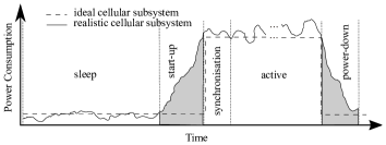
Typical cellular subsystem is comprised of sequential electronic blocks, where each building block’s functionality and availability are dependent on the previous blocks, posing an additional start-up time () and power-down time (). Therefore, in real settings during DRX, the cellular subsystem operates in five different phases, described as follows while being also marked in Fig. 1:
-
•
Sleep: in this phase, some of the hardware components in the cellular subsystem are either completely switched-off or operated in low-power modes. The exact components to be switched off are vendor-specific, and depend on DRX-cycle length. Generally, once in long DRX sleep (also known as deep sleep), the cellular subsystem keeps track of the number of frames by means of a low-power low-precision electronic oscillator (LPO);
-
•
Start-up: during transition from deep sleep to active state, the high-power high-precision oscillator (HPO) is switched-on. However, the HPO requires some time to settle and reach its optimum functionality, causing prolonged start-up time, and hence leading to the gradual rise in power consumption profile. Furthermore, it is paramount that the baseband (BB) synthesizer and the RF phase locked loop (PLL) are phase-matched [14]. Therefore, in addition to the switch-on delay of the HPO, also the PLL lock time contributes to the start-up time;
-
•
Synchronization: to assure that mobile device is in synchronization with the network, the mobile device needs to demodulate the synchronization signals, which are sent periodically (in case of LTE, every ms; configurable in 5G new radio (NR)). Meantime, the device can decode the system information, and also estimate the channel. The synchronization delay depends vastly on frame structure;
-
•
Active: in this phase, all hardware components in the cellular subsystem are fully switched-on, and synchronized, ready to receive PDCCH and physical downlink shared channel (PDSCH);
-
•
Power-down: powering down of integrated circuits of the BBU does not translate to the sharp turn-off, in other words, the cellular subsystem still consumes some power when turning off.
As a concrete example, Table III expresses the average transitional times and power consumption values of both short and long DRX cycles based on measurements of multiple different LTE cellular subsystems [7]. As can be seen, the sleep power consumption () is much higher in the short DRX cycle than in long one. This, in turn, has a direct influence on and . In case of short DRX, due to fact that BBU is ON during the sleep period, and are shorter than in long DRX. In short DRX cycle, the time required for synchronization, , is negligible. Required power for active state () varies based on IC/modem design, bandwidth, and other communication parameters.
| DRX Cycle | |||||
|---|---|---|---|---|---|
| short | mW | ms | mW | ms | ms |
| long | mW | ms | mW | ms | ms |
With respect to latency requirements, it is beneficial to process PDCCH in a very short DRX cycle to receive uplink (UL) grants or downlink (DL) data traffic, and promptly make an appropriate reaction. However, decoding the PDCCH requires a fast Fourier transform (FFT) whose size depends on the carrier bandwidth, and employs a blind decoding approach, where it hypothesizes over options of PDCCH locations [15, 16]. Especially for higher bandwidth carriers, the PDCCH rendering is very computationally intensive and power consuming. Therefore, decoding PDCCH frequently reduces the advantages of DRX, and high power consumption overhead is inevitable.
It has also been shown in [17] that the time period, that mobile device monitors the channel without any data allocation has a major impact on battery energy consumption. For instance, according to the experimental results, video streaming and web browsing traffic as the representative use cases have unscheduled PDCCH for % and % of time, respectively [17]. Furthermore, this problem is severe in unsaturated traffic scenarios, where many of the DRX cycles have eventually no data allocation for a particular mobile device. In general, there is also a trade-off between energy consumption and latency. That is, to reduce energy consumption, the DRX cycle needs to be made longer, which in turn leads to higher latency.
In this article, motivated by above, we propose a novel wake-up scheme as an efficient method to tackle the trade-off between latency and battery lifetime by reducing the power overhead of the DRX procedure, caused by unscheduled DRX cycles, while still maintaining low latency.
3 Wake-up Methods State of the Art
The related wake-up scheme works can be classified based on the wireless communication system (WSN, WLAN and cellular), for which the wake-up scheme is been developed. The original works on the wake-up methods are mainly focusing on WSNs and IoT-oriented WLANs, where the energy constraints of the end nodes are very tight. In spite of the promising foreseen evolution of the wake-up scheme in cellular communication systems, the wake-up concept needs to be studied further for the latter, and has started to raise interest recently also in 3GPP standardization. In this section, based on the existing works and documentations, the state-of-the-art is reviewed briefly.
3.1 WSN and WLAN Systems
Authors in [18, 19, 20, 21], developed different wake-up schemes. Previous works on WRx-empowered WSNs can be classified into the continuous and duty cycled channel monitoring. Continuous monitoring scenario prominently tackles use cases, where ultra-low latency of wireless nodes is the major requirement [18, 19]. However, in case of infrequent packets, energy consumption of the wireless node is remarkably high, and WRx can drain the battery energy if operating on continuous basis. Recently, duty-cycled ultra low-power WRx for WSNs has been developed [10], building on periodic wake-up beacons, which are transmitted ahead of data packets for synchronization of the communicating nodes. Mazloum et al. [10] also calculated closed-form expressions for the corresponding detection and false-alarm probabilities.
Demirkol et al [21] provided a comprehensive overview and insight into WRx, and investigated the benefits achieved with WRx along with the challenges observed in WSNs. In addition, they presented an overview of state-of-the-art hardware and networking protocol proposals as well as classification of WRx schemes. Moreover, authors in [22] introduced the concept of wireless-powered wake-up receiver, reducing the energy consumption of the wireless node considerably. The proposed receiver scavenges the RF energy from the received signal to power its sensor, communication and processing blocks. The proposed scheme can be utilized for a wide range of energy-constrained wireless applications such as wireless sensor actuator networks and machine-to-machine communications.
On WLAN system standardization side, IEEE 802.11 working group is currently considering WRx as a companion radio for the main receiver [23]. The major chip and wireless players such as Intel, MediaTek, and Ericsson have presented technical contributions to include WRx in IoT use cases, consistently [24, 25, 26]. It is expected that WRx operation will be fully standardized for IEEE 802.11 during 2020. In advocated proposal, WRx receives and decodes a wake-up packet without any help from the main receiver [27]. It has a cascaded wake-up signalling structure to support multiple stations. Furthermore, payload of wake-up packet is modulated with on-off keying because of its simplicity, although it is known to be prone to noise [27].
3.2 Cellular Systems
While WRx concepts have been extensively studied in WSN context, there are only a very few works available for scheduled frame-based cellular communication systems. Very recently, [7, 28] showed that the concept of WRx, when adapted to cellular communication, can provide % lower energy consumption. Authors in [7] combined microsleep, DRX and discontinuous transmission, and an aperiodic sleep mode to enhance battery lifetime of G mobile devices. However, the wake-up signaling structure and associated processing solutions are not addressed. Recently, the authors in [29] and [30], enhanced the DRX by enabling 5G mobile device to read small pre-grant message during active time, instead of executing full PDCCH processing. The preliminary numerical results show that such a scheme can reduce power consumption of mobile devices considerably, at the cost of negligible increments in signaling overhead.
Authors in [31] developed a wake-up scheme for machine-type communication (MTC) with idle mode emphasis. The approach builds on a separate standalone receiver for wake-up signal processing, while mathematical analysis and system parameter optimization were not pursued. The reported achievable misdetection rate is ca. 2% while the corresponding false alarm rate is 5.3%. The study and the proposed scheme did not address synchronization aspects nor synchronization assistance to the BBU.
Wake-up based solutions have started to raise interest recently also in 3GPP mobile network standardization. Specifically, a wake-up scheme to optimize the LTE-based enhanced-MTC (eMTC) and narrow-band IoT (NB-IoT) deployments were recently introduced in Rel. 15 [32]. The assumed wake-up concept is based on a narrowband indicator signal, transmitted over the available symbols of the configured subframes. It conveys unique cell identities, as per the narrowband secondary synchronization signal (SSS). Furthermore, the wake-up signal is scrambled by cell-specific code for mitigation of inter-cell interference [33]. The proposed wake up scheme for eMTC and NB-IoT is applied in idle mode before monitoring paging signaling and optimized for small infrequent packet transmissions ranging between some to bytes, a few times per day, and the wake-up scheme parameters are configured by higher layers [15]. Due to the promising power saving efficiency of such wake-up concept, it is also considered as the starting point in some 5G NR power saving studies, as discussed in [34]. Generally, because 5G NR supports very high speed data rates, the user plane data profile tends to be bursty and served in very short duration, and hence wake-up scheme can trigger user equipment (UE) for network access from power saving mode. Hence, the work and methods in this manuscript are very well inline with the upcoming 5G NR standardization efforts, and can be seen as an attempt to define, explore and analyze a concrete wake-up scheme towards the future releases of 5G NR, basically applicable for idle, inactive and connected modes.
Finally, it is noted that the original wake-up concepts in the WSN context are commonly based on unlicensed and contention-based channel access, while cellular communication systems build on scheduled frame-based access. Additionally, the processing capabilities, cost and power consumption of WSN nodes, overall, are commonly much lower than those of the cellular devices, especially mobile broadband capable UEs. Thus, also the available WRx power budget and assumed processing capabilities are substantially lower in WSN context, in general. As optimizing the power consumption is the highest priority in WSN context, one may also argue that the corresponding WRx solutions may even deactivate some of the receiver active components, such as the low noise amplifier (LNA). This leads to power consumption values in the range of a few W, compared to the WRx power consumption range of a few tens of mW in the cellular context [7]. LNA deactivation together with other hardware issues easily lead to substantially reduced WRx sensitivity, compared to the sensitivity requirements of cellular devices [21]. Finally, the observation time of the wake-up signal in WSN-related wake-up designs, commonly ranging in few tens of milliseconds, is substantially longer than the available observation time for cellular communication which is in the range of sub-milliseconds. The long observation time increases, among others, the buffering delay of the wake-up scheme.
4 Proposed Wake-up Scheme
4.1 Operating Principle at High Level
In general, depending whether an RRC connection is established or not, the proposed wake-up scheme described in this article can be adopted for idle, inactive or connected modes. However, for presentation brevity, we mainly focus on the connected mode in the following.Independent of the proposed wake-up scheme, successful completion of the cell search and selection procedures as well as acquiring initial system information and synchronization are required. The synchronization procedure occurs, in general, in two stages. In the first stage, the device acquires symbol timing, frequency offset, and cell ID using the primary synchronization signal (PSS). Then, in the second stage, the mobile device detects the frame boundary, physical cell group, and the cyclic prefix (CP) length by using the SSS [11].
Each mobile device in the connected mode operates in either the power-active or the power-saving mode. In the former, the device can receive or transmit in a continuous manner, which is appropriate, e.g., for ultra-reliable low latency communication (URLLC) purposes. In the latter, which is the focus of this work, the mobile device is configured with the proposed wake-up signaling and associated WRx in order to save battery lifetime, suitable for eMBB services as well as for massive machine-type communication (mMTC) services, which commonly contain small amounts of data at short intervals.
In the power-saving mode, the overall proposed wake-up scheme works as follows. Within a wake-up cycle, referred to as the w-cycle in the continuation with length denoted by , the WRx monitors the so-called physical downlink wake-up channel (PDWCH) for a specific on-duration time () to determine if any data is scheduled for it or not. Occasionally, based on either expiration of the configurable wake-up timer or interrupt signal from WRx, the BBU switches on, and thereon may (re)acquire synchronization, decodes both PDCCH and PDSCH, and performs connected-mode procedures such as reporting channel state and neighboring cell measurements to the network.
Because of the very simple hardware architecture of WRx, as discussed more extensively in Section 7, the start-up and power-down periods for WRx are extremely short. As elaborated more in the next subsection and Section 5, the processing requires demodulation of the specific subcarriers of only one or few OFDM symbols in each w-cycle, with overall duration of , in contrast to normal DRX, where BBU needs to operate full bandwidth for multiple symbols. In other words, narrowband reception of wake-up signaling requires much less signal processing, consequently needing also less memory and operations. Moreover, its narrowband signal structure, addressed in more details in the following subsection, has improved sensitivity due to its low in-band receive noise. Thus, it can be effectively applied and processed even in the presence of severe path loss and multipath propagation.
The length of the w-cycle, , can also be flexibly reconfigured and thus shortened, at the cost of reasonable extra energy consumption, and thus the adoption of the proposed wake-up scheme and the NM can also facilitate low communication latencies when properly configured. Additionally, built-in self-synchronizing signal structure and the utilization of the HPO remove the need for separate synchronization stage for WRx. Moreover, WRx can assist the BBU to obtain synchronization immediately, leading to further reduction in energy consumption and latency (i.e., , see Fig. 1 and Table III).
In order to identify when to wake up the BBU, the WRx monitors the PDWCH every w-cycle. The wake-up signaling structure transmitted every w-cycle is a unique code sequence, sent as a wake-up indicator (WI) for a mobile device that needs to wake up. Once there is packet arrival from core network to gNB, the gNB sends WI=1 to UE in upcoming wake-up instance. When such a WI has been sent to WRx, the network expects the corresponding mobile device to decode the PDCCH with time offset of . In other words, PDWCH indirectly informs WRx of potential scheduling on PDCCH with time offset of () or rather if it can skip interrupting BBU for the rest of . In order to improve the reliability of the wake-up scheme, once WI has been sent, the network will send additional WIs to the mobile device every w-cycle until the network receives proper ACK message. Similarly, the WRx can basically carry on the reception of PDWCH, according to the prevailing w-cycle pattern, after identifying WI=1 until receiving the target PDCCH message. Fig. 2 depicts the operation and power consumption of the proposed NM at principal level, while also illustrating the conventional DRX-enabled cellular subsystem operation for reference.

After receiving the PDCCH message at active state for on-time duration of , BBU initiates its inactivity timer for duration of . After the inactivity timer is initiated, and if a new PDCCH message is received before the expiration of , BBU re-initiates its inactivity timer. However, if there is no PDCCH message received before expiration of the inactivity timer, a sleep period starts, and NM switches to its sleep state, while WRx operates according to its w-cycle.
Due to the presence of noise, interference, distortion or mis-synchronization over PDWCH, two different WI errors, namely misdetection (wrongly detecting WI as ) and false alarm (wrongly detecting WI as ), are inevitable. False alarm can cause unnecessary power consumption of the BBU, while misdetection can add the buffering delay and wastes radio resources. Therefore, the requirements for both the probability of misdetection () and the probability of false alarm () are generally strict, in the order of %. Simulation results in Section 8, verify that the proposed scheme, building on the signaling structure and decoder principle described in Section 5, can achieve very low and for SNRs even below dB.
It is additionally noted that in the proposed wake-up scheme, if WRx does not detect WI for consequent w-cycles, referred to as the wake-up timer, it is assumed that the BBU will be switched on to perform connected mode procedures in order to eliminate the scenario that WRx is out of synchronization. While doing so, the UE can also report channel state information, as well as to perform general mobility procedures based on needs. The value of the wake-up timer can be configured by the network at device level based on, e.g., UE category, UE maximum mobility, traffic type and/or type of the network deployment. For instance, in case of ultra-dense networks, handovers may happen very frequently, thus the value of the wake-up timer can be configured to be fairly small to make sure mobility management is not compromised. Additionally, 5G systems should support also very high mobility levels, thus as shown in [35], UE channel measurements need to be reported fairly often, otherwise handover failure rate increases largely. Properly set wake-up timer removes thus the possibility that UE is forced to interrupt its ongoing connection due to exiting the serving cell coverage area and entering the new cell without handover procedures, which would lead to poor QoS and executing computationally-expensive and time-consuming tasks of cell selection and camping. At an other extreme, with e.g. zero-mobility IoT sensors, the value of can be set substantially larger to optimize the energy saving, within the limits of feasible synchronization. In our work, we prioritize the support for high-mobility UEs and assume a practical example wake-up timer value of ms (i.e. ). We emphasize that this is just one example numerical selection, and in practice the value of the wake-up timer can be configured by the network.
4.2 Frame and Signal Structures
In this work, overall and in the numerical evaluations, we consider LTE and 5G NR like frame structure, where transmission over the subcarriers is arranged into radio frames of ms long, each of which is divided into ten equally-sized individual subframes. Furthermore, we assume that each subframe is consisting of consecutive OFDM symbols while the subcarrier spacing is assumed to be kHz [11]. The OFDM symbol has samples, where is the CP length of the symbol, and is the number of samples of the body of the OFDM symbol. Additionally, within each frame, PSS and SSS are used for synchronization purposes. In this work, the introduced wake-up scheme is adopted for the aforementioned frame structure, in the context of frequency-division duplexing (FDD) networks, while it can also be generalized to other potential frame structures easily.
The proposed signaling is based on the G base station, commonly called gNB, transmitting a set of Zadoff-Chu (ZC) signatures with different cyclic shifts over a dedicated and pre-reported set of subcarriers, carrying set of WIs along with synchronization. A pool of known cyclic shift sequences is allocated to each gNB within a cell with a cell-specific root index, providing low inter-cell interference. The ZC sequences are known to have ideal cyclic auto-correlation, which is important for obtaining an accurate timing estimation and WRx identification. Additionally, the cross-correlation between different sequences based on cyclic shifts of the same ZC root sequence is zero as long as the cyclic shift used when generating the sequences is larger than the maximum DL propagation time in the cell plus the maximum delay spread of the channel [9].
The root ZC sequence, denoted by , is a polyphase exponential ZC sequence with root index of , and can be formulated as
| (1) |
where refers to the length of sequences, assumed odd, and needs to be integer larger than and relatively prime with respect to [36]. An odd-length ZC sequence is symmetric to its center element, and enables design of hardware-efficient approach for its generation. Further, if is prime, the discrete Fourier transform (DFT) of is another ZC sequence, denoted as . In [37] closed-form expressions for the DFT of cyclically shifted ZC sequences of arbitrary length are obtained. For the sake of readability, root index notation is omitted in the rest of the paper.
PDWCH is transmitted within the first symbol of subframe corresponding to the w-cycle. The main reason for transmitting PDWCH in the first symbol is to provide adequate time () for WRx to possibly switch on BBU as early as possible. Therefore, BBU can prepare to decode PDCCH, and eventually, demodulate and decode PDSCH. This reduces the processing delay, and thus the overall DL transmission delay. Furthermore, to support full power transmission in order to have robust communication, WIs are spread over adjacent subcarriers to reduce the power differences while at the same time providing the energy necessary for accurate reception also at cell-edge WRxs. To fulfill this, the multiple WIs are code multiplexed to a set of pre-defined subcarriers, which enables efficient usage of radio resource elements, while also reducing the power consumption of the WRx. We refer to a set of WIs transmitted on the same set of subcarriers as a PDWCH group.
The WRx can derive the resource elements in the control region where PDWCH is mapped by reading PDWCH group index value implying root index value of ZC sequence, and frequency offset parameter (difference relative to be DC bin or channel center-frequency). Each carrier or, equivalently each cell may have none, one or multiple PDWCH groups, adjusting to match the PDWCH demand, depending on the number of overall WRxs and carrier bandwidth. For instance, in case of ultra-dense networks, where small number of connected mobile devices may monitor PDWCH through their WRxs, the required number of PDWCH group is one, and a larger part of the DL control can accommodate L1/L2 control signaling.
The PDWCH parameters, i.e., the PDWCH group index and the unique cyclic shift within group of a given WRx, as well as the parameters for determining the frame number and subframe numbers in which the PDWCH is available can be signaled by higher layers. For this purpose, RRC message can be used by the network to configure, activate and deactivate wake-up scheme and the corresponding parameters on a per device basis. In order to reduce signaling overhead, the configuration parameters of the WRxs can vary semi-statically, and independently for each WRx, in order to absorb the dynamics of the network. In the rest of this article, for presentation and notational simplicity, we assume that there is only one PDWCH group.
4.3 RRC Modes and Signaling
In general, the wake-up based NM concept is agnostic to the RRC modes, and can thus be adopted for idle mode (where delay bound is in range of some hundreds of milliseconds), inactive mode (delay bound being in range of a few tens of milliseconds [7]) and the connected mode. The initial downlink timing synchronization is required when the NM moves to power saving mode. Once the NM has acquired the synchronization through PSS and SSS, the NM signals its capabilities ( and ) to the network. Then, the NM sends a wake-up scheme request as service to gNB and 5G core network. In response, QoS requirements (e.g., the maximum delay bound) and traffic pattern of ongoing connection are provided into gNB. Then, based on QoS requirements and other parameters (such as traffic arrival rate, delay bound, power profiles and start-up/power-down periods), the gNB configures the wake-up scheme parameters (, , , , , the PDWCH group index and the unique cyclic shift within group). After configuring the wake-up parameters, the gNB may send WI in pre-known wake-up instants, while the NM listens to the PDWCH with period of . Once WI equals to one, the gNB sends user data and corresponding signaling (PDCCH and PDSCH) to the target UE with timing offset of . Fig. 3 illustrates the overall procedure and the involved essential signaling at connected mode.
In general, the DRX and the wake-up scheme have similar procedures for parameter configuration. However, one of the main advantages of wake-up scheme over DRX is the need for reduced parameter re-configurations. For given delay requirements, NM can satisfy delay requirements with fixed parameter configuration for broad traffic variations, while DRX is very sensitive to traffic changes, and essentially requires re-configuration of its parameters frequently. The frequent re-configuration of DRX parameters to adapt to the traffic dynamics can, in turn, largely increase control signaling overhead, while also increases the UE energy consumption due to decoding the corresponding control signaling. By utilizing the wake-up scheme, energy consumption of NM can be reduced with properly configured wake-up parameters without additional signaling overhead. Furthermore, for application areas such as MTC, where sensors can be aperiodically polled by either a user or a machine, the traffic will have very non-periodic patterns. For such scenarios, the DRX may not fit well, while the wake-up scheme has more suitable characteristics being more robust and agnostic to the traffic type.

Finally, it is noted that since the PDWCH is mapped onto a set of adjacent subcarriers with the other subcarriers being used by DL control data symbols, PDWCH should be extracted from DL signal before the detection stage. This requires a filtering operation of the received signal, increasing the hardware complexity to some extent, and can also lead to slight performance degradation since the contribution of the rest of the DL control subcarriers cannot be totally filtered out due to the spectral leakage. To alleviate this issue, additional subcarriers in both sides of PDWCH are assumed to be muted.
5 Wake-up Signal Detection
5.1 Basics
We consider a multi-user scenario, where each sequence within PDWCH group is chosen from a set of cyclic-shifted ZC sequences with length of . Furthermore, during first OFDM symbol of predefined subframe, contiguous subcarriers are utilized while the exact location of PDWCH is indicated by the frequency offset parameter. For simplicity, we assume that subcarriers with relative indices to the DC subcarrier are used for PDWCH. Therefore, the DFT of the PDWCH group signal, denoted by , covering mobile devices in the cell can be expressed as
| (2) |
where
| (3) |
and for is a binary variable, representing the WI of the mobile device with its unique cyclic shift of , where . Additionally, is assumed to be always transmitted within the PDWCH group, helping WRx to retain synchronization even if . In Eq. (3) and in the rest of the article, modulo- indexing is assumed. The PDWCH signal structure is illustrated in Fig. 4.

In NM, the HPO is assumed to be kept ON during the connected mode, therefore the implications of clock drift are likely to be small during the w-cycles. In order to further reduce the impact of any possible residual clock drift, the proposed receiver has two-stage mechanism to recover any potential symbol time offset (STO) and carrier frequency offset (CFO). Specifically, at the first stage, which is performed in pre-FFT domain (time domain), maximum likelihood (ML)-estimator is applied to identify STO and fractional CFO. After the synchronization of the symbol timing, CP is removed correspondingly, and the second stage is performed in the FFT domain. In this stage, -point FFT () is applied to jointly detect integer CFO and WI. Moreover, because of decoding PDWCH in every w-cycle, WRx updates and compensates for time and frequency offsets every w-cycle, hence sustaining orthogonality among the subcarriers. The involved processing aspects are described next, in details.
5.2 First Stage: Initial Synchronization
The initial synchronization stage handles the potential STO and fractional CFO by exploiting intrinsic redundancy in CP of each OFDM symbol, as originally proposed in [38]. The CFO, normalized by the subcarrier spacing, is decomposed into integer CFO component () and the fractional CFO part (), where and . Similarly, STO () is the integer-valued relative time offset of the OFDM symbol in terms of sample instants.
WRx observes and collects samples of the received signal () within sliding sample observation window with length of . As shown in Fig. 5, the window contains one OFDM symbol with unknown arrival time . Then, based on well-known ML technique [38], WRx estimates both and .
The initial correction subsystem uses a numerically controlled oscillator (NCO) to generate an appropriate complex conjugated phasor, which is then multiplying the received signal to correct for the fractional CFO. After fractional CFO compensation, is applied to correct for positioning of the CP removal. Due to the potential remaining timing uncertainty, the truncated OFDM symbol contains either noise-corrupted copy of PDWCH data or DL data payload. The block diagram of the first stage processing is illustrated in the left part of Fig. 6.
5.3 Second Stage: Final Synchronization and Wake-Up Detection
Assuming that the initial synchronization provides an adequate orthogonality between subcarriers, the output of an -point FFT at the OFDM symbol, considering only the used/active subcarriers, is represented as . Under the assumption that is the index of the OFDM symbol carrying the PDWCH, can be written as
| (4) |
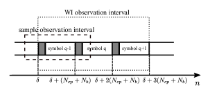
where denotes residual timing error, normalized by the sampling period, is the channel frequency response at the subcarrier, refers to the integer CFO, and is a circularly-symmetric white Gaussian noise process with average power . Without loss of generality and for notational simplicity, we assume that is incorporated into , therefore in the following, from Eq. (4) is removed and absorbed as part of . Due to the ambiguity of the arrival time of the OFDM symbol carrying the PDWCH, the WRx must observe a consecutive set of FFT outputs , in order to locate the PDWCH symbol. The corresponding WI observation window is shown in Fig. 5.
In general, in the second stage, the WRx needs to perform three tasks, namely 1) to acquire the position of the PDWCH symbol (), 2) to estimate the integer CFO (), and 3) to decode the WI (). In the following, we first introduce an estimation method of the unknown parameters building on correlation-based processing and energy maximization. Then, we address how the actual detection of the WI bit () can be carried out by utilizing the same correlation and energy quantities. The overall block diagram of the WRx processing, including both the first and the second stages, is shown in Fig. 6.
5.3.1 Final Synchronization
In the proposed approach, the WRx benefits from ideal cyclic auto- and cross-correlation properties of the ZC sequences by computing the received signal’s power delay profile (PDP) through a frequency-domain matched filter. For this purpose, the squared absolute value of the correlation of the received OFDM symbol with cyclic- and and phase-shifted root ZC sequences is given by
| (5) |
where is the time-domain sequence corresponding to and represents the integer frequency shift of ZC sequence. Building on the ideal cyclic auto- and cross-correlation properties of ZC sequences, the for all lags () reaches the maximum at the correctly estimated CFO () and PDWCH symbol index (). In order to reduce the implementation complexity, a hybrid time/frequency domain method is considered for the second stage. Using the properties of FFT, can be equivalently computed as
| (6) |
where is the discrete periodic correlation function of the received signal and the complex conjugate of frequency-shifted version of the root ZC sequence, evaluated at lag .
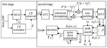
To further substantiate on the processing details, after removing CP at the first stage, and obtaining initial synchronization, is translated to the frequency domain by using an -point FFT, as shown in Fig. 6. The subcarriers corresponding to PDWCH are extracted from the output of the FFT by using a subcarrier demapper. The result of subcarrier demapping () is multiplied by the complex-conjugated root ZC sequences with potential frequency offsets (), and the result is properly oversampled by factor of by padding zeros in order to balance between detection performance and implementation complexity. Next, the IFFT block transforms the product of and from frequency into time domain. After that, the PDP samples are calculated by squaring the absolute value of the time-domain samples (). The received energy within the sliding window corresponding to interval , belonging to OFDM symbol can therefore be written as
| (7) |
Once the PDP samples of all potential frequency offsets of the root ZC sequence are obtained, all per frequency offset per OFDM symbol are calculated, and the corresponding frequency offset and the index of the OFDM symbol of the maximum received energy are chosen as estimates of and , respectively.
5.3.2 WI Detection
Next we address how the above same energy quantities can be directly utilized in the actual WI detection. Under the assumption that the samples in the sliding window in the absence of WI are uncorrelated Gaussian noise samples with variance , the samples of also present Gaussian distribution with zero mean and variance of . Consequently, has a central Chi-squared distribution with degrees of freedom with noise floor of . Therefore, the absolute WI detection threshold () can be calculated under the hypothesis of absence of WI as where is the cumulative distribution function (CDF) of , and can be modeled as a central Chi-squared random variable with degrees of freedom [39]. Without loss of generality, we can assume that , where is the threshold relative to the noise floor . By doing such, dependency of on the noise variance is removed (i.e. ), and can be expressed as
| (8) |
where is a pre-computed coefficient which can thus be stored in memory.
Similarly, the noise power samples at the input to noise floor estimation follows a central Chi-square distribution with degrees of freedom, expressed as
| (9) |
In above, is the relative detection threshold for noise floor estimation, and is set as follows
| (10) |
while the absolute noise floor threshold () can be computed as
| (11) |
Finally can be estimated as [40]
| (12) |
where the accumulation is over all samples less than , and is the number of available samples.
Then by utilizing a sliding window, if the received energy of the estimated OFDM symbol in interval () exceeds the WI detection threshold (), the WRx decodes , otherwise .
To sum up, are obtained as follows
| (13) |
and then
| (14) |
assuming that is restricted to a given parameter space . As can be seen, accurate realization of the estimator in Eq. (13) requires a search over values where denotes the number of considered FFT outputs and refers to the maximum span of subcarriers for which the integer CFO estimate is sought. For example, assuming that the integer CFO can be a maximum of subcarriers, then . The essential processing ingredients are summarized in Fig. 6.
6 Power Consumption and Delay Analysis
In this Section, the power states of NM are modeled as a semi-Markov process, and then its average buffering delay and average power consumption are calculated. Furthermore, the mathematical models shown in this section give an insight into the operation and the parameter configuration of the wake-up scheme. Our approach for analysing both the power consumption and delay characteristics of the wake-up scheme is similar to the DRX analysis presented in [41]. Thus, our models and approach deliberately build on similar notations to the work in [41], for readers’ convenience. It is also noted that in the proposed WRx concept, the inevitable misdetections and false alarms increase the buffering delay and energy consumption, respectively, which are properly reflected in the analysis.
For analytically tractability, the ETSI traffic model [42] is applied, which is widely used in various analytical and simulation studies related to 3GPP mobile radio networks. In the employed traffic model, a packet service session contains one or several packet calls with exponentially distributed session inter-arrival time (), while each packet call’s arrival time () follows exponential distribution. Moreover, each packet call consists of a sequence of packets with exponentially distributed packet inter-arrival time () within the packet call.
Additionally, based on the ETSI traffic model, at any time, the upcoming packet call belongs to either ongoing session or is the initial packet call of a new session with probabilities of and , respectively. It is obvious that the number of packet calls per a session () and number of packets per a packet call () follow geometric distribution, hence and [41]. In the rest of this article, the following equation is used for statistical characterization of both the packet call and the packet service session
| (15) |
where represents either or which are the mean packet call arrival rate and the mean session arrival rate, respectively. In addition, represents either or .
6.1 Semi-Markov Model
Four power states, namely, active-on timer (S0), active-inactivity timer (S1), WRx-ON (S2), and sleep (S3) are modeled by a semi-Markov process, as shown in Fig. 7. Briefly, the states and corresponding transitions between them are described as follows:
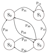
-
•
Active-on timer (S0): when NM is at S0, NM is able to receive data. Any packet arrival during S0 initiates , and NM moves to S1. Otherwise at the expiry of , the NM moves to S3;
-
•
Active-inactivity timer (S1): when NM is at S1, is running, and if it is scheduled before the expiry of , it restarts and remains at S1, otherwise it transfers to S3. Additionally, at S1, NM functions fully, and is able to decode PDCCH and PDSCH;
-
•
WRx-ON (S2): at this state, WRx monitors PDWCH; if WRx receives WI=, NM transfers to S3, otherwise (WI=) it transfers to S0;
-
•
Sleep (S3): at this state, NM is asleep and is unable to receive any data. Moreover, NM at the end of sleep cycle moves to S2, unless WRx has been at S2 and S3 for consecutive w-cycles, hence moving to S0.
Because of the relativity short inter-packet arrival time within a packet call of eMBB-like sessions, for simplicity of analytical formulations, we can assume that once a packet call starts, NM serves all packets without transitioning to a new state. Similar assumption was adopted in DRX context in [41]. Assume now that denotes the transition probability from to . When NM is at , and if NM receives data before the expiry of , it moves to , otherwise it moves to . Thus, and can be calculated as
| (16) |
and
| (17) |
When NM is at , it restarts if next packet starts before expiry of , otherwise it moves to . Therefore, and can be calculated as follows
| (18) |
and
| (19) |
When NM is at , it moves to either because of false alarm or correct detection, otherwise it moves to . Therefore and can be calculated as follows
| (20) |
and
| (21) |
where is sleep period per w-cycle, i.e., .
Similarly, and , where , for , is the probability of decoding WI for times as , and can be calculated as follows
| (22) |
Let , be the steady state probability that NM is at . By utilizing the set of balance equations () and the sum of probabilities equation (), , can be solved easily. Due to space limitations, only the final equations are written herein, without intermediate steps, as
| (23) |
| (24) |
| (25) |
| (26) |
The holding times for are represented as . For , NM may stay for at this state (no arriving packet), or due to a packet arrival before expiry of , it moves to . Therefore, can be written as a function of time as follows
| (27) |
and thus
| (28) |
where and are the probability density functions of exponential distributions of inter-packet call and inter-session arrival time, respectively, which are of the form and .
Furthermore, with the assumption of utilizing stop-and-wait hybrid automatic request flow control algorithm (which can be modeled as an M/M/ queuing model), can be written as follows [43]
| (29) |
where is the average processing time for transmitting all packets of a packet call, and is the average time of inactivity timer after serving an ongoing packet call, referred to as the average inactivity period. The processing time consists of serving packets with a per-packet service time of , which is the time interval from transmission of a packet from gNB to getting ACK from the mobile device. According to Wald’s Theorem [44]
| (30) |
where and are the average number of packets within a packet call and the mean packet arrival rate within a packet call, respectively. Additionally, if a packet arrives before , inactivity period equals the inter-packet call time, otherwise the inactivity period equals . Therefore, the inactivity period () can be calculated as a function of as follows
| (31) |
while can be expressed as
| (32) |
Additionally, the holding times for and are fixed, and therefore and .
6.2 Average Power Consumption Calculation
In order to develop an analytical model for power saving achieved by NM, we assess the average power consumption of NM (). Assuming , , denotes the power consumption of NM at state , the average power consumption can be expressed as
| (33) |
where E denotes the consumed average energy during overall observation time (T), and can be calculated as
| (34) |
In above, is the average required energy for transitional states, and can be calculated as , where and are the required energies for transitioning of NM from sleep to fully active and vice versa, respectively.
Additionally, can be calculated as follows
| (35) |
where is the mean overall time period that NM spends on transitional periods, i.e., .
In next sections, concrete example numerical values of power and energy consumption of different states are presented (cf. particularly Table IV).
6.3 Average Delay Calculation
We assume that the packets that arrive during and are buffered at gNB until NM enters to , causing some buffering delay. The overall delay experienced by end users consists of server delay, core network delay, buffering delay and scheduling delay. However, considering all these in analytical work complicates the system model largely making it intractable. Thus, for the purpose of the analytical work, the server and core network delays are ignored. Furthermore, without loss of generality, we assume that the radio access network experiences non-fully-loaded traffic conditions, and thus all packets that arrive during and can be served promptly without further scheduling delay. Ignoring the packet scheduling contribution to the overall delay is a valid assumption when there are adequate radio resources per TTI that can accommodate the data packets of target UEs, while in other cases it is a simplification.
Now, in order to have a feasible and intuitive delay analysis and expressions, a packet arrival time during and is assumed to belong to one of the two following intervals, 1) between first and w-cycles, or 2) during after w-cycles, where for all cycles, WI= is decoded. In the former case, the average buffering delay () is caused by a packet that arrives on w-cycle, where , with the numbering starting from the first w-cycle straight after transition from S0 or S1 to S3. This delay can be calculated as follows
| (36) |
While in the latter case, the average buffering delay of a packet () arriving after w-cycles, where for all w-cycles, WI is decoded as , can be calculated as
| (37) |
Finally, by combining Eq. (36) and Eq. (37), and using the corresponding probabilities of first and second intervals, the overall average buffering delay (), imposed by the wake-up scheme, can be written as
| (38) |
Due to resulting fairly long expressions, the explicit substitutions of (22), (36) and (37) into (38) are omitted.
7 Overall Receiver Architecture and
Implementation Aspects
For the completeness of the study, before going into the numerical performance evaluations, we provide in this section selected implementation insight regarding how the proposed WRx processing can be efficiently incorporated into the overall new modem (NM) hardware. Even though the finest implementation details and optimization are outside the scope of this paper, fairly elaborate implementation aspects are reported and discussed in order to understand the concept feasibility and particularly the realistic power consumption characteristics of the WRx unit. Further specifics regarding the power consumption details are provided as supplementary material in the Appendix.
7.1 WRx Implementation Fundamentals
The NM, illustrated at principal implementation level in Fig. 8, provides all corresponding radio and signal processing tasks for the wake-up concept, while naturally also handles the typical cellular subsystem functionalities. In general, typical cellular BB processing needs dedicated digital application-specific integrated circuits (ASICs) as well as one or multiple processors to perform the defined signal processing and protocol stack tasks. However, owing to the low processing complexity of the proposed wake-up scheme, the WRx functionalities can be implemented directly in radio frequency integrated circuit (RFIC), providing reduced power consumption, higher integrity, and fast access as well as essentially negligent start-up and power-down periods. Furthermore, as fetching data from external processor through RF-digital interface is time and power consuming, the RFIC-based implementation of the wake-up detection is favored also in this sense.
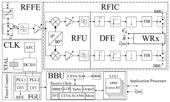
The embedment of the WRx on RFIC is generally enabled by the recent advances in the low-cost and power-efficient CMOS technology, allowing also selected digital functionalities to be implemented directly on RFIC. Additionally, modern RFICs are highly reconfigurable over most of their building blocks, providing high flexibility. Such flexibility is particularly interesting in the context of the wake-up scheme, as both the bandwidth and the gain performance can be adapted for the reception of the wake-up signaling. Furthermore, the placement of the WRx at digital domain of the RFIC permits multiple filter bandwidths to be included without any essential penalty in the silicon area. Thus, the WRx helps for maintaining synchronization of the overall NM, while carries the wake-up signal processing. Similar to the BBU, WRx receives the complex I/Q samples from digital front-end (DFE) on chip. Furthermore, WRx utilizes the processing and memory capabilities of the RFIC, together with a dedicated FFT/IFFT block, in order to detect the WI. The configuration of the radio frequency front-end (RFFE) and RFIC is controlled at several stages, through applicable software, in WRx and BBU via control links.
For further details related to task specific aspects, the readers are referred to the Appendix.
|
power state |
RFFE |
RFU |
DFE |
WRx |
CLK |
FGU |
BBU |
Interface |
Others |
PW |
|---|---|---|---|---|---|---|---|---|---|---|
| S3 | 0 | 0 | ||||||||
| S2 | ||||||||||
| S0/S1 |
7.2 Measurement-based Power Consumption
Next, measurement based experimental power consumption model of the overall NM is presented, building on 16nm CMOS implementation when it comes to the RFIC. As defined in Section 6, the NM operation contains essentially four states, namely, S0, S1, S2 and S3. In general, in a given state, the overall power consumption comprises of a number of components. Furthermore, depending on the specific NM state, some components may be either ON or OFF. In general, within S0 or S1, NM’s power consumption vastly depends on the operating bandwidth, while the power consumption values in S2 and S3 are essentially independent of the bandwidth since a fixed resource of subcarriers each of width kHz are assumed for the PDWCH, as further detailed in the Appendix.
Table IV represents an experimental power consumption breakdown of the NM’s main hardware components assuming the basic channel bandwidth of MHz. Our methodology for profiling the energy consumption builds on the physical power measurements, assessing the current and voltage of the resistors on the power supply rails of the relevant components on real hardware. As can be observed through Table IV, the proposed WRx, including both radio and digital processing, consumes only some mW of power. This is generally a very low power consumption figure. Additionally, Table IV details how this figure is contributed by the different subcomponents or modules. It is noted that the power consumption values utilized to evaluate the proposed scheme, reported in Table IV, are based on actual prototype hardware, while certainly the finalized products may still differ, being further improved and optimized in their final hardware and software solutions. Hence, these numbers utilized in the paper can be considered indicative, and representative, while the final products are beyond our scope. Furthermore, for readers’ convenience, some further clarifications and details regarding the different modules and their design choices, considered in the power consumption experiments are provided as supplementary material in the Appendix.
Finally, it is noted that for the purpose of synchronization, during sleep period, RFFE, RFU and BBU are switched off, but HPO is ON, and a timer/counter is used to track the location of the starting symbol of the PDWCH subframe. Therefore, the energy expenditure for sleep state in NM is slightly higher than that in a typical cellular subsystem. Power consumption of cellular subsystem is mainly dependent on its implementation. The overall NM entity consumes about mJ and mJ in average for the duration of the corresponding start-up and power-down times of ms and ms, respectively. Moreover, as discussed in Section 4, the proposed NM assists the BBU to obtain synchronization immediately, leading to (see Fig. 1).
8 Numerical Results and Analysis
Numerical evaluations are next conducted to assess and illustrate the performance of the presented wake-up scheme. The wake-up receiver detection performance is first analysed, through empirical simulations, followed by the system energy saving and latency evaluations where also comparisons to the analytical results are made.
8.1 Basic Assumptions
The radio frame and assumed hardware settings for simulations and numerical evaluations follow directly the assumptions made already in Sections 4-7. Specifically, the basic MHz carrier bandwidth case with kHz subcarrier spacing is considered, while the radio frame duration is assumed to be 10 ms. For channel modeling, we adopt the GPP extended pedestrian A model (EPA) [45].
Each simulation scenario lasts for frames, and is repeated for times in order to collect statistically reliable results. Each PDWCH group has users, utilizing ZC sequences with length of and root index of . Moreover, we assume that .
Stemming from the high-precision oscillator assumption, the oscillator deviation can be assumed to be within ppm in room temperature. Thus, the clock drifting and CFO are very small within the duration of a single w-cycle. Even at a higher carrier frequency of say GHz, the maximum CFO stemming from the ppm accuracy is kHz, corresponding to the case that the gNB’s LO and the NM’s LO both have the largest allowed yet opposite-sign frequency deviations. This is less than twice the assumed subcarrier spacing, thus we set the value of the configurable parameter in the integer CFO estimation to . Additionally, OFDM symbols is considered.
In general, in the energy saving and latency evaluations, the WRx configuration in terms of the w-cycle and different timers as well as the traffic model assumptions have all an impact on achievable performance figures. Baseline parameter configurations and traffic model assumptions, following those in [41], [46], are listed in Table V. Many of these parameter values are also varied in the evaluations, in order to better understand and assess the power consumption and latency characteristics of the considered wake-up based system, and the potential involved dependencies. Finally, the measurement-based power consumption values, shown in Table IV for the different states, are used.
| Parameter | Value |
|---|---|
| wake-up cycle, | ms |
| on-time duration, | ms |
| inactivity timer, | ms |
| offset time, | ms |
| average session inter-arrival time, | s |
| average packet-call inter-arrival time, | s |
| average packet inter-arrival time, | s |
| average number of packet calls per session, | |
| average number of packets per packet-call, |
8.2 Wake-up Receiver Detection Performance
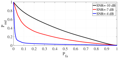
We begin by addressing the reliability of the wake-up signal detection at WRx, together with the achievable synchronization performance, with specific emphasis on challenging low-SNR conditions. Fig. 9 shows the receiver operating characteristic (ROC) curve of the proposed wake-up signaling and detection scheme under the EPA channel model at three different SNR values of dB, dB, and dB, respectively. As it can be expected, for all three ROC curves, there is a clear trade-off between the achievable probability of missed detection, , and the probability of false alarm, . By comparing the ROC curves corresponding to the different SNRs, and assuming that the target false alarm probability is %, we can observe that very reliable wake-up signal detection can still be obtained at an SNR of dB while the detection performance is then sharply degrading for lower SNRs of dB and dB.
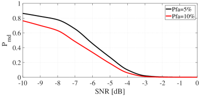
The further assess the detection performance and its dependency on the SNR as well as on the constraint, additional numerical results are provided in Fig. 10. Specifically, the figure shows the behavior of the for varying SNR with two different constraints, namely 5% and 10%. The figure clearly illustrates that very reliable wake-up signal detection can be achieved down to SNRs in the order of dB, depending on the exact detection probability target. For SNRs yet lower than these, the performance degrades clearly. Additionally, as expected, the misdetection rate for a lower false alarm rate constraint is higher than the corresponding misdetection rate of higher false alarm rate, at any given SNR. This implies the need for configuring the target false alarm rate individually for different use cases based on their energy and delay requirements.
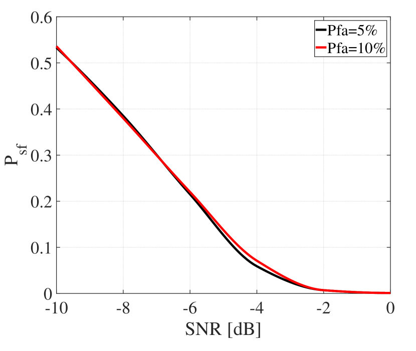
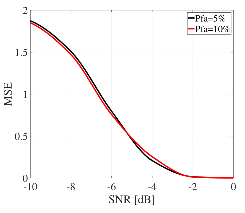
Next, Fig. 11(a) and Fig. 11(b) illustrate the obtained synchronization failure rate () performance, and the achieved mean squared error (MSE) of the CFO estimate as a function of SNR, respectively. As can be observed, the failure rate reduces for increasing SNR, while very high-quality synchronization can be obtained down to SNRs of some dB. Interestingly, the synchronization failure rate is not dependent on constraint. The main reason is that is estimated without utilizing the target based threshold. We note that the detection results in Figs. 9 and 10 contain also the impacts of the synchronization procedures, hence illustrating reliably the achievable detection performance.
Moreover, because of utilizing PDP values for selecting or identifying the PDWCH symbol index, the probability of detection of the correct PDWCH OFDM symbol is almost %, even for low SNRs in the order of - dB, and is thus not explicitly illustrated. The PDPs of other OFDM symbols are extremely low compared to that of the PDWCH symbol. It is in general very vital to have large PDWCH detection rate, since misdetection of the PDWCH symbol index would directly increase both the false alarm rate and the misdetection rate of the wake-up signaling. We note that also the PDWCH symbol index detection is built in to the results in Figs. 9 and 10, while not illustrated separately.
It is additionally noted that the false alarm and misdetection rates are essentially independent of the w-cycle, unless the w-cycle is very long, say tens of seconds, which could cause the frequency and/or time offsets to be eventually larger than the chosen values of and . In contrast, it is also noted that the overall numbers of false alarm and misdetection events, within a given overall time window, do indeed increase when the w-cycle reduces. Similarly, the impact of the value of on the false alarm and misdetection rates is essentially negligible. This is due to the fact that even when identifying WI=1, the WRx is assumed to carry on the PDWCH reception, according to its w-cycle, until receiving the target PDCCH message.
8.3 Energy Saving and Latency Performance
Next, the energy consumption and latency characteristics of the wake-up based system are assessed. We use and evaluate the analytical results, obtained in Section 6, while also simulate and compare corresponding empirical results. The baseline values for the wake-up scheme parameters are those shown in Table V, while many of them are also again varied. Additionally, the measurement based power consumption values, shown in Table IV for the different states, are used. Regarding the assumed wake-up signal detection performance in the analysis, four pairs of false alarm and misdetection rates are considered, building on the results obtained in the previous subsection. Specifically, we consider the following examples cases, obtained from Fig. 10:
-
•
% and % (SNR of dB),
-
•
% and % (SNR of dB),
-
•
% and % (SNR of dB),
-
•
% and % (SNR of dB).
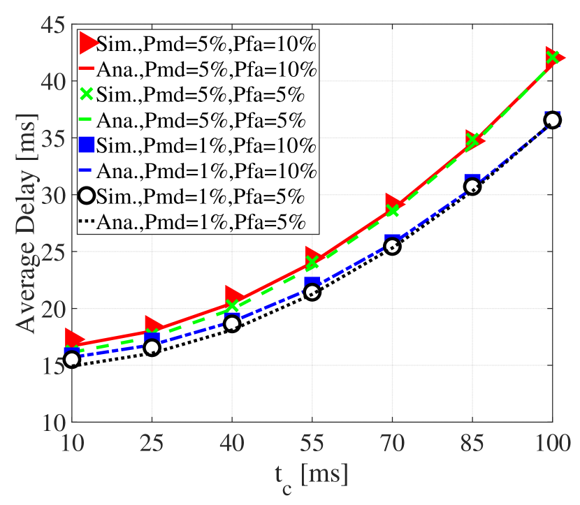
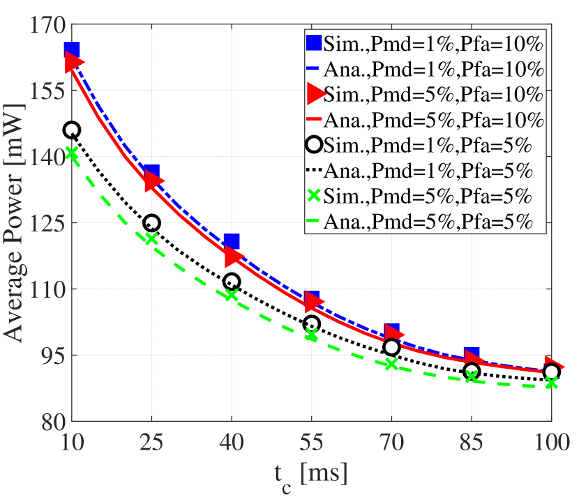
Fig. 12 then illustrates the obtained average buffering delay and the power consumption of the NM for varying values of the w-cycle. First, it can be observed that the results of the theoretical analysis are very consistent and similar with the empirical ones, for both the average delay and power consumption characteristics, verifying the accuracy of the analytical results. For given values of and , longer w-cycles increase latency due to longer buffering in each cycle as depicted in Fig. 12(a), hence shorter w-cycles are favorable for delay sensitive applications. However, reducing the w-cycle increases the energy consumption substantially. The main reasons for such energy consumption increase in the considered NM concept are (i) more frequent switching of the BBU, and (ii) the small but nonzero power overhead of WRx. From Fig. 12, we can also observe that the empirical buffering delay and power consumption values are always slightly higher than the corresponding analytical results. Thus, the analytical models are essentially lower bounds for the NM delay and power consumption, the main reason for such trend being the simplifying assumptions related to the packet calls service time made in the analytical work. However, generally speaking, the analytical and empirical results are very well inline.
As it can also be observed in Fig. 12(a), higher for a given , increases the buffering delay. This is very natural, since misdetection means that the incoming PDSCH data transmission window is missed. Furthermore, an impact of on the buffering delay is less tangible. The main reason for this is that after a false alarm, the NM can still decode PDWCH. Fig. 12(b) also clearly shows that a higher , for a given , increases the energy consumption, due to unnecessarily waking up the BBU.
Next, the effects of the on-time duration, , on the average delay and power consumption are illustrated in Fig. 13, for different values of and . According to Fig. 13(a), the value of has a relatively small impact on the average delay. That is, increasing the value of reduces the average delay but only to a small extent. In contrast, as shown in Fig. 13(b), the effect of the value of on the power consumption is more notable. This is because in the event of a false alarm, the UE remains unnecessarily in the active stage for the duration of , and thus the larger the value of , the larger is the additional energy consumption. Thus, we conclude that overall it is more beneficial to use relatively small values of .
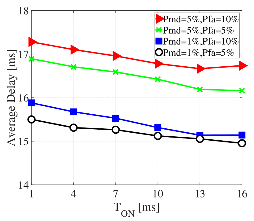
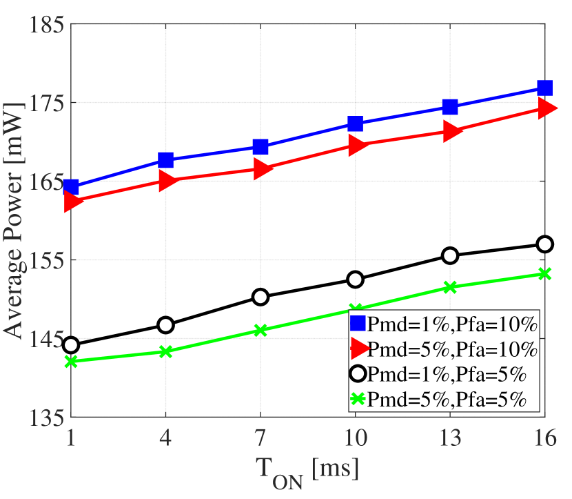
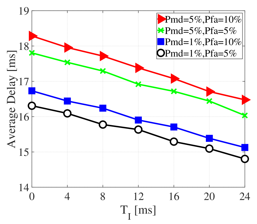
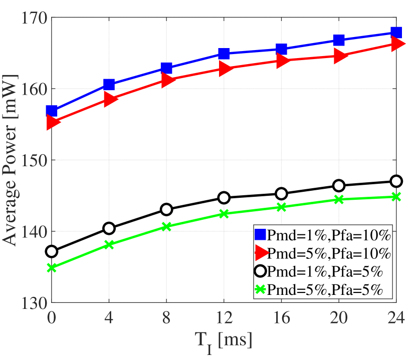
Fig. 14 then illustrates and assesses how the value of the inactivity timer, , affects the average delay and power consumption under different detection scenarios. From Fig. 14(a), we can see that a longer results in a shorter delay. However, a longer results also in a higher probability for wasting energy due to absence of any packet, while BBU is fully active. Moreover, for lower , the average delay increases noticeably. The figure thus illustrates the impact and importance of correct configuration of on both the delay and power consumption, depending on traffic parameters.
8.4 Comparison with DRX
Finally, the performances of the developed NM and a DRX-enabled reference cellular subsystem are compared, for different values of the w-cycle and the short/long DRX cycle lengths. We assume that the w-cycle and the short-DRX cycle vary from to ms and from to ms, respectively. In addition, for fair comparison, we assume that the DRX long cycle is four times of its short DRX cycle, and also that the short DRX timer is ms. Similar assumptions are made also, e.g., in [7], [41], [47].
Fig. 15 shows the achievable average power consumption versus the average delay, for two different values of the mean packet arrival rate. We can observe that when the w-cycle and the short-DRX cycle are increased, from to ms and from to ms, respectively, the average packet delay increases while the power consumption reduces. This is natural because when increasing the w-cycle or the short-DRX cycle, the sleep ratio increases, and thus power consumption is reduced but at the cost of an extra delay. Moreover, for given delay requirement, and per power saving mechanism (wake-up scheme or DRX), power consumption for the higher packet arrival rate ( packets/ms) is larger than that for the lower packet arrival rate ( packets/ms). This is mainly because the larger value of implies more packets arriving at gNB during a given time interval. This, in turn, makes the UE BBU more likely to stay in the active state, leading to a higher power consumption for a given delay constraint. Interestingly, for given power consumption, and per power saving mechanism, the delay for packets/ms is larger than that for packets/ms. At first glance, it may sound contradictory to the aforementioned reasoning that UE has lower sleep ratio for higher packet arrival rate. However, one should keep in mind that in order to have equal power consumption values for two different packet arrival rates, the w-cycle or DRX-cycle need to be lower for lower packet arrival rate, and as result the overall delay is shorter for lower packet arrival rate under a fixed power consumption value.
In general, as it can be observed in Fig. 15, for delay requirements within 10 ms to 60 ms, the NM consumes much less power than a DRX-based UE. For instance, if the buffering delay constraint is ms, by utilizing DRX, mobile device may achieve average power consumption of mW, while with employing NM, this can be reduced down to mW at . This represents power savings in the order of 30%, which is a substantial number. It is also observed that DRX works better for applications which can tolerate very long delays (large sleep-ratio), the reason being that the NM consumes more energy in the sleep state than DRX based UE in the deep sleep state of long DRX cycle. Though this difference may change if the WRx power consumption is pushed further down.
Finally, based on Fig. 15, we also acknowledge that DRX can better satisfy very short delay requirements, mostly due to the fact that the start-up time of cellular subsystem for short-DRX cycle is less than ms [7], [41], [47]. In case of the NM, due to the wake-up scheme’s offset time, achieving such very low latencies in the order of 1-5 ms is difficult. Additionally one can observe that for tighter delay constraints, both methods consume higher amounts of energy, the main reason being that the cellular subsystem remains in active state more often than in case with longer delay constraints.
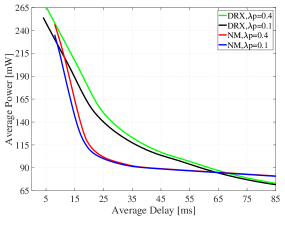
9 Conclusions
In this article, a timely wake-up radio based access scheme was studied, developed and analyzed, in order to facilitate improved mobile device power-efficiency vs. latency trade-offs in future 5G and beyond systems. Specifically, an efficient wake-up signaling structure was developed, such that reliable wake-up detection can be achieved even in challenging conditions with negative SNRs. Additionally, efficient receiver processing solutions, building on the proposed wake-up signal structure, were also described, for joint synchronization and wake-up symbol location estimation purposes, as well as to decode the actual wake-up indicator bit. We also addressed the wake-up receiver hardware and implementation aspects, while also analyzed the system power consumption and latency characteristics analytically in closed-form. A large collection of representative numerical results was also provided, evidencing that very reliable wake-up signal detection can be achieved even at negative SNRs. Additionally, the numerical results showed that the delay and power consumption characteristics are functions of the involved wake-up cycle and the related parameters, allowing for the system optimization per application such that desired balance between the power-efficiency and latency is achieved. Finally, it was shown that up to reduction in the mobile device power consumption can be obtained, for given latency characteristics, compared to the existing DRX-based solutions, when latencies in the order of 10-60 ms are considered. Our future work will focus on the wake-up system and WRx parameter configuration optimization for different applications and corresponding traffic characteristics. Additionally, further optimized solutions and hardware development are pursued to push down the WRx energy consumption even further.
References
- [1] S. Rostami, K. Heiska, O. Puchko, J. Talvitie, K. Leppanen, and M. Valkama, “Novel wake-up signaling for enhanced energy-efficiency of 5G and beyond mobile devices,” in Proc. IEEE GLOBECOM 2018, Dec. 2018, pp. 1–7.
- [2] F. Boccardi, R. W. Heath, A. Lozano, T. L. Marzetta, and P. Popovski, “Five disruptive technology directions for 5G,” IEEE Communications Magazine, vol. 52, no. 2, pp. 74–80, February 2014.
- [3] G. Fettweis and S. Alamouti, “5G: Personal mobile internet beyond what cellular did to telephony,” IEEE Communications Magazine, vol. 52, no. 2, pp. 140–145, February 2014.
- [4] H. Jayakumar, K. Lee, W. S. Lee, A. Raha, Y. Kim, and V. Raghunathan, “Powering the Internet of Things,” in Proc. ACM ISLPED 2014. New York, NY, USA: ACM, 2014, pp. 375–380.
- [5] “Designing mobile devices for low power and thermal efficiency,” Qualcomm Technologies, Inc., Tech. Rep., Oct. 2013.
- [6] A. Carroll and G. Heiser, “An analysis of power consumption in a smartphone,” in Proc. USENIXATC2010. Berkeley, CA, USA: USENIX Association, 2010, pp. 21–21.
- [7] M. Lauridsen, “Studies on mobile terminal energy consumption for LTE and future 5G,” Ph.D. dissertation, Aalborg University, 2015.
- [8] “IMT traffic estimates for the years 2020 to 2030,” ITU-R, Tech. Rep., July 2015.
- [9] S. P. Erik Dahlman and J. Skold, 4G LTE/LTE-Advanced for Mobile Broadband. Academic Press, 2011.
- [10] N. S. Mazloum and O. Edfors, “Performance analysis and energy optimization of wake-up receiver schemes for wireless low-power applications,” IEEE Transactions on Wireless Communications, vol. 13, no. 12, pp. 7050–7061, Dec 2014.
- [11] S. Parkvall, E. Dahlman, A. Furuskar, and M. Frenne, “NR: The new 5G radio access technology,” IEEE Communications Standards Magazine, vol. 1, no. 4, pp. 24–30, Dec 2017.
- [12] S. Rostami, K. Arshad, and P. Rapajic, “Optimum radio resource management in carrier aggregation based LTE-advanced systems,” IEEE Transactions on Vehicular Technology, vol. PP, no. 99, pp. 1–1, 2017.
- [13] M. Gupta, S. C. Jha, A. T. Koc, and R. Vannithamby, “Energy impact of emerging mobile internet applications on LTE networks: issues and solutions,” IEEE Commun. Mag., vol. 51, no. 2, Feb. 2013.
- [14] M. Lauridsen, L. Noel, T. Sorensen, and P. Mogensen, “An empirical LTE smartphone power model with a view to energy efficiency evolution,” Intel Technology Journal, vol. 18, no. 1, pp. 172–193, 2014.
- [15] “Evolved universal terrestrial radio access (E-UTRA); physical layer procedures,” 3GPP, TS36.213, Tech. Rep., Mar. 2019.
- [16] “Evolved universal terrestrial radio access (E-UTRA); user equipment (UE) procedures in idle mode,” 3GPP, TS 36.304, Tech. Rep., Jan. 2016.
- [17] “UE power consideration based on days-of-use,” Qualcomm Incorporated, R1-166368, Tech. Rep., Aug. 2016.
- [18] M. Lont, D. Milosevic, P. G. M. Baltus, A. H. M. van Roermund, and G. Dolmans, “Analytical models for the wake-up receiver power budget for wireless sensor networks,” in Proc. IEEE GLOBECOM 2009, Nov 2009, pp. 1–6.
- [19] Y. Zhang, L. Huang, G. Dolmans, and H. de Groot, “An analytical model for energy efficiency analysis of different wakeup radio schemes,” in Proc. IEEE PIMRC 2009, Sept 2009, pp. 1148–1152.
- [20] E. Y. A. Lin, J. M. Rabaey, and A. Wolisz, “Power-efficient rendez-vous schemes for dense wireless sensor networks,” in Proc. IEEE ICC 2004, vol. 7, June 2004, pp. 3769–3776 Vol.7.
- [21] I. Demirkol, C. Ersoy, and E. Onur, “Wake-up receivers for wireless sensor networks: benefits and challenges,” IEEE Wireless Communications, vol. 16, no. 4, pp. 88–96, Aug 2009.
- [22] S. Rostami, K. Heiska, O. Puchko, K. Leppanen, and M. Valkama, “Wireless powered wake-up receiver for Ultra-Low-Power devices,” in Proc. IEEE WCNC 2018, Barcelona, Spain, Apr. 2018.
- [23] “Low-power wake-up receiver for 802.11,” IEEE 802.11-15/1307r1, Tech. Rep.
- [24] “Low-power wake-up receiver follow-up,” IEEE 802.11-16/0341r0, Tech. Rep.
- [25] “Discussion of wake-up receivers for lrlp,” IEEE 802.11-16/0381r0, Tech. Rep.
- [26] “Lp wur wake-up packet identity considerations,” IEEE 802.11-16/0402r0, Tech. Rep.
- [27] “Proposal for wake-up receiver (wur) study group,” IEEE 802.11-16/0722r0, Tech. Rep.
- [28] M. Lauridsen, G. Berardinelli, F. M. L. Tavares, F. Frederiksen, and P. Mogensen, “Sleep modes for enhanced battery life of 5G mobile terminals,” in Proc. IEEE VTC 2016 Spring, May 2016, pp. 1–6.
- [29] S. Rostami, K. Heiska, O. Puchko, K. Leppanen, and M. Valkama, “Robust Pre-Grant signaling for Energy-Efficient 5G and beyond mobile devices,” in Proc. IEEE ICC’18 GCSN, Kansas City, USA, May 2018.
- [30] S. Rostami, K. Heiska, O. Puchko, K. Leppanen, and M. Valkama, “Pre-grant signaling for energy-efficient 5G and beyond mobile devices: Method and analysis,” IEEE Trans. on Green Commun. and Networking, vol. 3, no. 2, pp. 418–432, June 2019.
- [31] R. P. K. Ponna and D. Ray, “Saving energy in cellular IoT using low-power wake-up radios,” Master’s thesis, Lund University, 2018.
- [32] “Evolved universal terrestrial radio access (E-UTRA) and evolved universal terrestrial radio access network (E-UTRAN); overall description,” 3GPP, TS 36.300, Tech. Rep., Mar. 2019.
- [33] “Evolved universal terrestrial radio access (E-UTRA); physical channels and modulation,” 3GPP, TS 36.211, Tech. Rep., Mar. 2019.
- [34] “New SID: Study on UE power saving in NR,” 3GPP, RP-181463, Tech. Rep., June. 2018.
- [35] “Mobility enhancements in heterogeneous networks,” 3GPP TR 36.839 V11.0.0, Tech. Rep., Sep. 2009.
- [36] J. C. Guey, “The design and detection of signature sequences in time-frequency selective channel,” in Proc. IEEE PIMRC 2008, Sept 2008, pp. 1–5.
- [37] B. M. Popovic, “Efficient DFT of Zadoff-Chu sequences,” Electronics Letters, vol. 46, no. 7, pp. 502–503, April 2010.
- [38] J. J. van de Beek, M. Sandell, and P. O. Borjesson, “ML estimation of time and frequency offset in OFDM systems,” IEEE Transactions on Signal Processing, vol. 45, no. 7, pp. 1800–1805, Jul 1997.
- [39] J. G. Proakis and D. K. Manolakis, Digital Signal Processing (4th Edition), 4th ed. Prentice Hall, Apr. 2006.
- [40] S. Sesia, I. Toufik, and M. Baker, LTE, The UMTS Long Term Evolution: From Theory to Practice. Wiley Publishing, 2009.
- [41] A. T. Koc, S. C. Jha, R. Vannithamby, and M. Torlak, “Device power saving and latency optimization in LTE-A networks through DRX configuration,” IEEE Transactions on Wireless Communications, vol. 13, no. 5, pp. 2614–2625, May 2014.
- [42] “Universal mobile telecommunications system (UMTS); selection procedures for the choice of radio transmission technologies of the UMTS,” UMTS 30.03 TR 101 112, V3.1.0, Tech. Rep., Apr. 1998.
- [43] L. Kleinrock, Theory, Volume 1, Queueing Systems. Wiley-Interscience, 1975.
- [44] R. Nelson, Probability, Stochastic Processes, and Queueing Theory: The Mathematics of Computer Performance Modeling, 1st ed. Springer Publishing Company, Incorporated, 2010.
- [45] “LTE; evolved universal terrestrial radio access (E-UTRA); relay radio transmission and reception,” 3GPP TS 36.16 version 11.4.0 Release 11, Tech. Rep., Apr. 2015.
- [46] W. A. Khan, “Impact of DRX on VoIP performance and battery life in LTE,” Master’s thesis, Blekinge Inst. Tech., Jan. 2009.
- [47] C. Tseng, H. Wang, F. Kuo, K. Ting, H. Chen, and G. Chen, “Delay and power consumption in LTE/LTE-A DRX mechanism with mixed short and long cycles,” IEEE Transactions on Vehicular Technology, vol. 65, no. 3, pp. 1721–1734, March 2016.
- [48] J. Rust, T. Wiegand, and S. Paul, “Design and implementation of a low complexity NCO based CFO compensation unit,” in Proc. EUSIPCO 2012, Aug 2012, pp. 116–120.
- [49] M. Keating, D. Flynn, R. Aitken, A. Gibbons, and K. Shi, Low Power Methodology Manual: For System-on-Chip Design. Springer Publishing Company, Incorporated, 2007.
- [50] S. He and M. Torkelson, “Designing pipeline FFT processor for OFDM (de)modulation,” in 1998 URSI International Symposium on Signals, Systems, and Electronics. Conference Proceedings (Cat. No.98EX167), Sep 1998, pp. 257–262.
![[Uncaptioned image]](/html/2001.00914/assets/x20.jpg) |
Soheil Rostami received the M.Sc. degree in Mobile Communication Systems with distinction from the University of Surrey, UK, in 2011. During 2012–2017, he was with the Faculty of Engineering and Science, University of Greenwich, UK, and with Nokia Bell Labs, Belgium. Since 2017, he has been working as a Researcher with 5G Radio Network Technologies team in Huawei Technologies Oy (Finland) Co., Ltd. In 2018, he was a Visiting Researcher with Centre Tecnològic de Telecomunicacions de Catalunya (CTTC), Spain. |
![[Uncaptioned image]](/html/2001.00914/assets/Kari_Heiska.jpg) |
Kari Heiska received the M.Sc. and Ph.D. degrees from the Helsinki University of Technology (HUT), Finland in 1992 and 2004, respectively. He was with the HUT Laboratory of Space Technology, Nokia Networks, Nokia Research Center and Digita in Finland. Currently he is working as a Senior Researcher at Huawei Technologies in Finland. |
![[Uncaptioned image]](/html/2001.00914/assets/OleksandrPuchko.jpg) |
Oleksandr Puchko received the M.Sc degree in wireless communication from Kharkiv National University of Radio Electronics in 2007, and the Ph.D degree in 2013 from the University of Jyvaskyla. During 2008–2017, he was working as a researcher for University of Jyvaskyla, Magister Solutions, Unikie and Huawei Technologies Oy (Finland). Since 2018 he is Engineer of the Hard Real Time Software for the 5G base station in Mobile Networks at Nokia. |
![[Uncaptioned image]](/html/2001.00914/assets/x21.jpg) |
Kari Leppanen received his M.Sc. and Ph.D. from Helsinki University of Technology, Finland, in 1992 and 1995, respectively, majoring in Space Technology and Radio Engineering. After graduation, he has worked in National Radio Astronomy Observatory (USA), Helsinki University of Technology (Finland), Joint Institute for VLBI in Europe (the Netherlands) and Nokia Research Center (Finland). Currently Kari leads the 5G Radio Network Technologies team at Huawei in Stockholm and Helsinki. |
![[Uncaptioned image]](/html/2001.00914/assets/Mikko_Valkama.jpg) |
Mikko Valkama (S’00–M’01–SM ’15) received the M.Sc. and Ph.D. Degrees (both with honors) in electrical engineering (EE) from Tampere University of Technology (TUT), Finland, in 2000 and 2001, respectively. In 2003, he was working as a visiting post-doc research fellow with the Communications Systems and Signal Processing Institute at SDSU, San Diego, CA. Currently, he is a Full Professor and Department Head at the newly established Tampere University (TAU), Finland. His general research interests include radio communications, radio localization and radio-based sensing, with emphasis on 5G and beyond mobile radio networks. |
Appendix: Further Implementation Details
This supplementary material provides further implementation details, related to the prototype hardware hardware.
Task Specific Aspects
The initial synchronization is performed by cross-correlating the signal with a delayed version of itself, and then applying a moving average filter with averaging length equal to the CP length. The maximum correlation magnitude, and the corresponding phase angle, are then measured in every OFDM symbol length. This means that the phase angle from the strongest correlation peak is registered, and is utilized to estimate the frequency offset. In this work, the hardware architecture proposed in [38] is adopted. It requires ca. and complex additions and multiplications, respectively.
To compensate for the CFO, an NCO is utilized to generate a complex phasor at the estimated frequency. The complex conjugated phasor is multiplied by the received signal to correct the frequency offset. In this work, the multipartite table method (MTM) is applied to implement arctangent function and sine/cosine generator. It is proven to be much faster, more accurate and more efficient in power and area compared with some alternative algorithms [48]. The NCO consists of a register accumulating the bit input values and a phase-to-sine mapper. In order to enable hardware-efficient signal processing, the full input phase range is scaled to values, and saved in internal memory of the RFIC. The phase accumulator produces a digital sweep with a slope proportional to the input phase. On the other hand, de-rotation must be performed, which can be easily achieved by vector rotation. For our work, we have selected modified radix- tree-multiplier structure [49], and segmentation is used.
The computational complexity of the WRx mainly comes from the IFFT and FFT blocks. In this work, radix- single-path delay feedback is adopted due to their ability to use the registers more efficiently by storing the one butterfly output in feedback shift registers. A single data stream goes through the multiplier at every stage [50]. This algorithm requires multipliers, radix- butterflies and registers. Its memory requirements are minimal.
Specifically, as detailed in Section 5, frequency-domain correlators with size of are needed to detect the parameter set. Correlations can generally be done using multiple IFFTs, at the expense of an increase in hardware complexity and cost, or a single IFFT at the expense of an increase in decision delay. The latter is appropriate for scenarios where the frequency drift is low, or the value of is low. Due to fact that ZC generation in real-time is computationally expensive, in our design the ZC sequence pre-computed by the BBU is buffered in the available memory of the RFIC to be used in the WRx.
In the WRx implementation, the BB signal is sampled at a rate of MHz, and converted to the frequency-domain through a -point FFT unit (). The PDWCH uses subcarriers for the signaling of the WI bits, and as guard subcarriers. Due to the use of the FFT and IFFT, the proposed WRx implementation has an inherent algorithmic latency of clock cycles at MHz. Furthermore, its start-up and power-down periods together are less than ms.
Additional Selected Issues
RFFE: An antenna, LNA, and SAW filter for channel selection are the main elements of RFFE used in the measurements.
RFU: The RFU downconverts the analog amplified received high-frequency signal to a low-frequency BB signal directly using single balanced mixer, channel selection filter and AGC; eventually, it passes the I/Q samples to the DFE. In the proposed NM design, the BB filters for channel selection are active op-amp based filters known as gyrators. Additionally, the BB AGC module monitors and averages the received signal strength, and adjusts the gain of the RFFE.
DFE: The DFE consists of ADC, DC offset cancellation, digital filter, and decimator. Because of narrow bandwidth of wake-up signaling, NM requires very low-lost conversion method; thus Sigma delta converter is utilized, which provides high dynamic range and high flexibility in converting diverse bandwidth input signals. Due to zero-IF architecture, DC offset removal is essential. A finite impulse response (FIR) filter is used to attenuate signals, and noise that are outside PDWCH subband. Finally, to eliminate redundant sampled data at the output of DFE, decimator is employed.
BBU: The BBU receives the digitized signal as complex I/Q samples from the analog to digital converter (ADC) via RF-BB interface. In our design for BB processing, a set of commercial modules are utilized, as it is seen in Fig. 8. To support receiver signal processing related tasks, one high-end DSP core (CEVA-XC) is employed along with a real-time processor (CEVA-X) for the physical layer coordination between the transmit and receiver subsystems, as well as overall BBU control. In conjunction, function-specific hardware accelerators are applied for different processing stages such as FFT, de-interleaver, ILR and etc. Additionally, for protocol stack execution, a quad-core high-performance real-time processor (Cortex R) is employed.
Digitally Controlled Crystal Oscillator, DCXO: NM uses a single high frequency crystal oscillator to generate accurate master clock ( MHz). DCXOs at the clock interface are utilized to adjust the reference frequency. Furthermore, frequency offsets are measured by BBU and WRx, and compensated through automatic frequency correction (AFC) module based on BBU and WRx.
Frequency Generation Unit, FGU: Different frequencies required in the NM are derived from the master clock using multiple PLLs. Local oscillator (LO) frequency for the mixer, the sampling frequency at the ADC, the clock signal for timer/counter, DFE, WRx and BBU are the main units that receive the clock.